ICGOO在线商城 > THS6072CDGN
 Datasheet下载
- 型号: THS6072CDGN
- 制造商: Texas Instruments
- 库位|库存: xxxx|xxxx
- 要求:
| 数量阶梯 | 香港交货 | 国内含税 |
| +xxxx | $xxxx | ¥xxxx |
查看当月历史价格
查看今年历史价格
THS6072CDGN产品简介:
ICGOO电子元器件商城为您提供THS6072CDGN由Texas Instruments设计生产,在icgoo商城现货销售,并且可以通过原厂、代理商等渠道进行代购。 提供THS6072CDGN价格参考¥21.68-¥40.28以及Texas InstrumentsTHS6072CDGN封装/规格参数等产品信息。 你可以下载THS6072CDGN参考资料、Datasheet数据手册功能说明书, 资料中有THS6072CDGN详细功能的应用电路图电压和使用方法及教程。
| 参数 | 数值 |
| 产品目录 | 集成电路 (IC)半导体 |
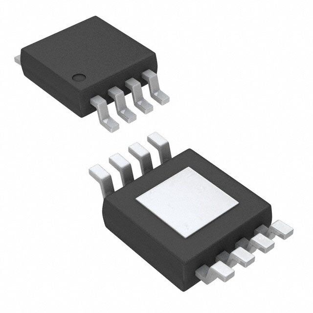
| 描述 | IC ADSL DIFF RCVR LP 8-MSOP高速运算放大器 Low-Power ADSL Diff Receiver |
| 产品分类 | |
| 品牌 | Texas Instruments |
| 产品手册 | |
| 产品图片 |
|
| rohs | 符合RoHS无铅 / 符合限制有害物质指令(RoHS)规范要求 |
| 产品系列 | 放大器 IC,高速运算放大器,Texas Instruments THS6072CDGN- |
| 数据手册 | |
| 产品型号 | THS6072CDGN |
| 产品目录页面 | |
| 产品种类 | |
| 供应商器件封装 | 8-MSOP-PowerPad |
| 共模抑制比—最小值 | 78 dB |
| 其它名称 | 296-24072-5 |
| 包装 | 管件 |
| 协议 | DSL |
| 单位重量 | 24.400 mg |
| 双工 | - |
| 商标 | Texas Instruments |
| 安装类型 | 表面贴装 |
| 安装风格 | SMD/SMT |
| 封装 | Tube |
| 封装/外壳 | 8-TSSOP,8-MSOP(0.118",3.00mm 宽)裸焊盘 |
| 封装/箱体 | HVSSOP-8 |
| 工作温度 | 0°C ~ 70°C |
| 工作电源电压 | 4.5 V to 16 V |
| 工厂包装数量 | 80 |
| 带宽 | 175 MHz |
| 接收器滞后 | - |
| 放大器类型 | Voltage Feedback Amplifier |
| 数据速率 | - |
| 最大功率耗散 | 2.14 W |
| 最大工作温度 | + 70 C |
| 最小工作温度 | 0 C |
| 标准包装 | 80 |
| 电压-电源 | 5 V ~ 15 V |
| 电源电压-最大 | 16 V |
| 电源电压-最小 | 4.5 V |
| 电源电流 | 5 mA |
| 稳定时间 | 43 ns |
| 类型 | 接收器 |
| 系列 | THS6072 |
| 转换速度 | 230 V/us |
| 输入补偿电压 | 7 mV |
| 输出电流 | 85 mA |
| 通道数量 | 2 Channel |
| 配用 | /product-detail/zh/THS6072EVM/296-10074-ND/380618/product-detail/zh/THS6092EVM/296-20568-ND/562147 |
| 驱动器/接收器数 | 0/2 |


- 商务部:美国ITC正式对集成电路等产品启动337调查
- 曝三星4nm工艺存在良率问题 高通将骁龙8 Gen1或转产台积电
- 太阳诱电将投资9.5亿元在常州建新厂生产MLCC 预计2023年完工
- 英特尔发布欧洲新工厂建设计划 深化IDM 2.0 战略
- 台积电先进制程称霸业界 有大客户加持明年业绩稳了
- 达到5530亿美元!SIA预计今年全球半导体销售额将创下新高
- 英特尔拟将自动驾驶子公司Mobileye上市 估值或超500亿美元
- 三星加码芯片和SET,合并消费电子和移动部门,撤换高东真等 CEO
- 三星电子宣布重大人事变动 还合并消费电子和移动部门
- 海关总署:前11个月进口集成电路产品价值2.52万亿元 增长14.8%


PDF Datasheet 数据手册内容提取
THS6072 LOW-POWER ADSL DIFFERENTIAL RECEIVER SLOS290B – FEBRUARY 2000 – REVISED JUNE 2001 (cid:0) ADSL Differential Receiver THS6072 – Ideal for Central Office or Remote D OR DGN PACKAGE Terminal Applications (TOP VIEW) (cid:0) Low 3.4 mA Per Channel Quiescent Current (cid:0) 1OUT 1 8 VCC+ 10 nV/√Hz Voltage Noise 1IN– 2 7 2OUT (cid:0) Very Low Distortion 1IN+ 3 6 2IN– – THD = –79 dBc (f = 1 MHz, RL = 1 kΩ) VCC– 4 5 2IN+ (cid:0) High Speed – 175 MHz Bandwidth (–3 dB, G = 1) – 230 V/µs Slew Rate (cid:0) Cross Section View Showing High Output Drive, IO = 85 mA (typ) PowerPAD Option (DGN) (cid:0) Wide Range of Power Supplies – V = ±5 V to ±15 V CC (cid:0) Available in Standard SOIC or MSOP PowerPAD Package (cid:0) Evaluation Module Available description The THS6072 is a high-speed, low-power differential receiver designed for ADSL communication systems. Its low 3.4-mA per channel quiescent current reduces power to half that of other ADSL receivers making it ideal for low power ADSL applications. This receiver operates with a very low distortion of –79 dBc (f = 1 MHz, R = 1 kΩ). The THS6072 is a voltage feedback amplifier offering a high 175-MHz bandwidth and L 230-V/µs slew rate and is unity gain stable. It operates over a wide range of power supply voltages including ±4.5 V to ±15 V. This device is available in a standard SOIC or MSOP PowerPAD package. HIGH-SPEED xDSL LINE DRIVER/RECEIVER FAMILY DEVICE DRIVER RECEIVER 5 V ±5 V ±15 V DESCRIPTION • • • • THS6002 500-mA differential line driver and receiver • • • THS6012 500-mA differential line driver • • • THS6022 250-mA differential line driver • • • THS6032 500-mA low-power ADSL central-office line driver THS6042/3 • • • 350-mA, ±12 V ADSL CPE Line Drivers THS6052/3 • • • 100-mA, ±12 V ADSL CPE Line Drivers • • • • THS6062 Low-noise ADSL receiver • • • THS6072 Low-power ADSL receiver THS6092/3 • • • 200-mA, ±12 V ADSL CPE Line Drivers • • • THS7002 Low-noise programmable-gain ADSL receiver CAUTION: The THS6072 provides ESD protection circuitry. However, permanent damage can still occur if this device is subjected to high-energy electrostatic discharges. Proper ESD precautions are recommended to avoid any performance degradation or loss of functionality. Please be aware that an important notice concerning availability, standard warranty, and use in critical applications of TexasInstruments semiconductor products and disclaimers thereto appears at the end of this data sheet. PowerPAD is a trademark of Texas Instruments. PRODUCTION DATA information is current as of publication date. Copyright 2001, Texas Instruments Incorporated Products conform to specifications per the terms of Texas Instruments standard warranty. Production processing does not necessarily include testing of all parameters. POST OFFICE BOX 655303 • DALLAS, TEXAS 75265 1
THS6072 LOW-POWER ADSL DIFFERENTIAL RECEIVER SLOS290B – FEBRUARY 2000 – REVISED JUNE 2001 AVAILABLE OPTIONS PACKAGED DEVICES NUMBER OF MSOP EVALUATION TA CHANNELS SMAPLLL AOSUTTICLINE† PMLSAOSTPI†C SYMBOL MODULE (D) (DGN) 0°C to 70°C 2 THS6072CD THS6072CDGN AHZ THS6072EVM –40°C to 85°C 2 THS6072ID THS6072IDGN AIA — †The D and DGN packages are available taped and reeled. Add an R suffix to the device type (i.e., THS6072CDGN). functional block diagram VCC 1IN– 1OUT 1IN+ 2IN– 2OUT 2IN+ –VCC Figure 1. THS6072 – Dual Channel 2 POST OFFICE BOX 655303 • DALLAS, TEXAS 75265
THS6072 LOW-POWER ADSL DIFFERENTIAL RECEIVER SLOS290B – FEBRUARY 2000 – REVISED JUNE 2001 absolute maximum ratings over operating free-air temperature (unless otherwise noted)† Supply voltage, V . . . . . . . . . . . . . . . . . . . . . . . . . . . . . . . . . . . . . . . . . . . . . . . . . . . . . . . . . . . . . . . . . . . . ±16.5 V CC Input voltage, V . . . . . . . . . . . . . . . . . . . . . . . . . . . . . . . . . . . . . . . . . . . . . . . . . . . . . . . . . . . . . . . . . . . . . . . . . . ±V I CC Output current, I . . . . . . . . . . . . . . . . . . . . . . . . . . . . . . . . . . . . . . . . . . . . . . . . . . . . . . . . . . . . . . . . . . . . . . . 150 mA O Differential input voltage, V . . . . . . . . . . . . . . . . . . . . . . . . . . . . . . . . . . . . . . . . . . . . . . . . . . . . . . . . . . . . . . . . ±4 V IO Continuous total power dissipation . . . . . . . . . . . . . . . . . . . . . . . . . . . . . . . . . . . . . See Dissipation Rating Table Maximum junction temperature, T . . . . . . . . . . . . . . . . . . . . . . . . . . . . . . . . . . . . . . . . . . . . . . . . . . . . . . . . 150°C J Operating free-air temperature, T : C-suffix . . . . . . . . . . . . . . . . . . . . . . . . . . . . . . . . . . . . . . . . . . . 0°C to 70°C A I-suffix . . . . . . . . . . . . . . . . . . . . . . . . . . . . . . . . . . . . . . . . . . –40°C to 85°C Storage temperature, T . . . . . . . . . . . . . . . . . . . . . . . . . . . . . . . . . . . . . . . . . . . . . . . . . . . . . . . . . –65°C to 150°C stg Lead temperature 1,6 mm (1/16 inch) from case for 10 seconds . . . . . . . . . . . . . . . . . . . . . . . . . . . . . . . 300°C †Stresses beyond those listed under “absolute maximum ratings” may cause permanent damage to the device. These are stress ratings only and functional operation of the device at these or any other conditions beyond those indicated under “recommended operating conditions” is not implied. Exposure to absolute-maximum-rated conditions for extended periods may affect device reliability. DISSIPATION RATING TABLE PPAACCKKAAGGEE θJJAA θJJCC TAA = 25°C (°C/W) (°C/W) POWER RATING D 167‡ 38.3 740 mW DGN§ 58.4 4.7 2.14 W ‡This data was taken using the JEDEC standard Low-K test PCB. For the JEDEC Proposed High-K test PCB, the θJA is 95°C/W with a power rating at TA = 25°C of 1.32 W. §This data was taken using 2 oz. trace and copper pad that is soldered directly to a 3 in. × 3 in. PC. For further information, refer to Application Information section of this data sheet. recommended operating conditions MIN NOM MAX UNIT Dual supply ±4.5 ±16 SSuuppppllyy vvoollttaaggee, VVCCCC+ aanndd VVCCCC– VV Single supply 9 32 C-suffix 0 70 OOppeerraattiinngg ffrreeee-aaiirr tteemmppeerraattuurree, TTAA °°CC I-suffix –40 85 POST OFFICE BOX 655303 • DALLAS, TEXAS 75265 3
THS6072 LOW-POWER ADSL DIFFERENTIAL RECEIVER SLOS290B – FEBRUARY 2000 – REVISED JUNE 2001 electrical characteristics at T = 25°C, V = ±15 V, R = 150 Ω (unless otherwise noted) A CC L dynamic performance PARAMETER TEST CONDITIONS MIN TYP MAX UNIT VCC = ±15 V 175 GGaaiinn == 11 MMHHzz VCC = ±5 V 160 SSmmaallll-ssiiggnnaall bbaannddwwiiddtthh ((–33 ddBB)) VCC = ±15 V 70 GGaaiinn == –11 MMHHzz VCC = ±5 V 65 BBWW VCC = ±15 V 35 BBaannddwwiiddtthh ffoorr 00.11 ddBB ffllaattnneessss GGaaiinn == 11 MMHHzz VCC = ±5 V 35 FFuullll ppoowweerr bbaannddwwiiddtthh†† VO(pp) = 20 V, VCC = ±15 V 2.7 MMHHzz VO(pp) = 5 V, VCC = ±5 V 7.1 SSRR SSlleeww rraattee‡‡ VCC = ±15 V, 20-V step Gain = 5 230 VV//µµss VCC = ±5 V, 5-V step Gain = 1 170 VCC = ±15 V, 5-V step 43 SSeettttlliinngg ttiimmee ttoo 00.11%% GGaaiinn == –11 nnss VCC = ±5 V, 2-V step 30 tts VCC = ±15 V, 5-V step 233 SSeettttlliinngg ttiimmee ttoo 00.0011%% GGaaiinn == –11 nnss VCC = ±5 V, 2-V step 280 †Full power bandwidth = slew rate/2π VO(Peak). ‡Slew rate is measured from an output level range of 25% to 75%. noise/distortion performance PARAMETER TEST CONDITIONS MIN TYP MAX UNIT TTHHDD TToottaall hhaarrmmoonniicc ddiissttoorrttiioonn VOO((pp)) = 2 V,, VCC = ±15 V RL = 1 kΩ –79 ddBBcc f = 1 MHz, Gain = 2 VCC = ±5 V RL = 1 kΩ –77 Vn Input voltage noise VCC = ±5 V or ±15 V, f = 10 kHz 10 nV/√Hz In Input current noise VCC = ±5 V or ±15 V, f = 10 kHz 0.7 pA/√Hz Channel-to-channel crosstalk VCC = ±5 V or ±15 V, f = 1 MHz –75 dB dc performance PARAMETER TEST CONDITIONS MIN TYP MAX UNIT TA = 25°C 10 19 VVCCCC == ±±1155 VV, VVOO == ±±1100 VV, RRLL == 11 kkΩΩ VV//mmVV TA = full range 9 OOppeenn lloooopp ggaaiinn TA = 25°C 8 16 VVCCCC == ±±55 VV, VVOO == ±±22.55 VV, RRLL == 225500 ΩΩ VV//mmVV TA = full range 7 TA = 25°C 1 7 VVOOSS IInnppuutt ooffffsseett vvoollttaaggee mmVV TA = full range 8 Offset voltage drift TA = full range 15 µV/°C VCC = ±5 V or ±15 V TA = 25°C 1.2 6 IIIIBB IInnppuutt bbiiaass ccuurrrreenntt µµAA TA = full range 8 TA = 25°C 20 250 IIOOSS IInnppuutt ooffffsseett ccuurrrreenntt nnAA TA = full range 400 Offset current drift TA = full range 0.3 nA/°C 4 POST OFFICE BOX 655303 • DALLAS, TEXAS 75265
THS6072 LOW-POWER ADSL DIFFERENTIAL RECEIVER SLOS290B – FEBRUARY 2000 – REVISED JUNE 2001 electrical characteristics at T = 25°C, V = ±15 V, R = 150 Ω (unless otherwise noted) (continued) A CC L input characteristics PARAMETER TEST CONDITIONS MIN TYP MAX UNIT VCC = ±15 V ±13.8 ±14.1 VVIICCRR CCoommmmoonn-mmooddee iinnppuutt vvoollttaaggee rraannggee VV VCC = ±5 V ±3.8 ±3.9 VCC = ±15 V, VICR = ±12 V, TA = full range 78 90 dB CCMMRRRR CCoommmmoonn mmooddee rreejjeeccttiioonn rraattiioo VCC = ±5 V, VICR = ±2 V, TA = full range 84 93 dB RI Input resistance 1 MΩ CI Input capacitance 1.5 pF output characteristics PARAMETER TEST CONDITIONS MIN TYP MAX UNIT VCC = ±15 V RL = 250 Ω ±12 ±13.6 VV VCC = ±5 V RL = 150 Ω ±3.4 ±3.8 VVOO OOuuttppuutt vvoollttaaggee sswwiinngg VCC = ±15 V ±13 ±13.8 RRLL == 11 kkΩΩ VV VCC = ±5 V ±3.5 ±3.9 VCC = ±15 V 65 85 IIOO OOuuttppuutt ccuurrrreenntt†† RRLL == 2200 ΩΩ mmAA VCC = ±5 V 50 70 ISC Short-circuit current† VCC = ±15 V 100 mA RO Output resistance Open loop 13 Ω †Observe power dissipation ratings to keep the junction temperature below the absolute maximum rating when the output is heavily loaded or shorted. See the absolute maximum ratings section of this data sheet for more information. power supply PARAMETER TEST CONDITIONS MIN TYP MAX UNIT Dual supply ±4.5 ±16.5 VVCCCC SSuuppppllyy vvoollttaaggee ooppeerraattiinngg rraannggee VV Single supply 9 33 TA = 25°C 3.4 4.2 VVCCCC == ±±1155 VV TA = full range 5 IICCCC SSuuppppllyy ccuurrrreenntt ((ppeerr aammpplliiffiieerr)) mmAA TA = 25°C 2.9 3.7 VVCCCC == ±±55 VV TA = full range 4.5 PSRR Power supply rejection ratio VCC = ±5 V or ±15 V TA = full range 79 90 dB NOTE: Full range = 0°C to 70°C for C suffix and –40°C to 85°C for I suffix POST OFFICE BOX 655303 • DALLAS, TEXAS 75265 5
THS6072 LOW-POWER ADSL DIFFERENTIAL RECEIVER SLOS290B – FEBRUARY 2000 – REVISED JUNE 2001 TYPICAL CHARACTERISTICS OPEN LOOP GAIN & PHASE RESPONSE vs CROSSTALK FREQUENCY vs FREQUENCY 100.00 45° 20 80.00 0° VGCaiCn == 1±15 V 0 B RF = 0 Ω pen Loop Gain – d246000...000000 Phase Gain 1–934055°°°Phase Responce Crosstalk – dB ––4200 RL = 150 Ω O 0.00 180° –60 VCC = ±5 V and ±15 V –20.00 –225° –80 100 1k 10k 100k 1M 10M 100M 1G 100k 1M 10M 100M 1G f – Frequency – Hz f – Frequency – Hz Figure 2 Figure 3 TOTAL HARMONIC DISTORTION TOTAL HARMONIC DISTORTION SETTLING vs vs vs OUTPUT STEP FREQUENCY FREQUENCY –40 –40 330 c VCC = ± 15 V c VCC = ± 5 V dB Gain = 2 dB Gain = 2 290 n - –50 VO(PP) = 2 V n - –50 VO(PP) = 2 V Distortio –60 RL = 150 Ω Distortio –60 RL = 150 Ω e – ns 221500 VCC = ±5 V(0.01%) c c m moni –70 moni –70 ng Ti 170 VCC = ±15 V(0.01%) al Har –80 RL = 1 kΩ al Har –80 RL = 1 kΩ Settli 130 VCC = ±5 V(0.1%) D - Tot –90 D - Tot –90 5900 VCC = ±15 V(0.1%) H H T T –100 –100 10 1100.000k 1010M.00 101000M.00 1100.000k 1010M.00 101000M.00 2 3 4 5 f - Frequency - Hz f - Frequency - Hz VO – Output Step Voltage – V Figure 4 Figure 5 Figure 6 POWER SUPPLY REJECTION RATIO DISTORTION DISTORTION vs vs vs OUTPUT VOLTAGE OUTPUT VOLTAGE FREQUENCY B 0 –50 –50 o - d VCC = ±15 V & ±5 V 2nd Harmonic 2nd Harmonic Rati–20 –60 –60 ejection –40 –VCC on – dBc –70 3rd Harmonic on – dBc –70 3rd Harmonic upply R–60 +VCC Distorti –80 Distorti –80 S er R - Pow–80 –90 VRGCLa iCn= ==1 k5±Ω 15 V –90 VRGCLa iCn= ==1 5 5±0 1 Ω5 V R f = 1 MHz f = 1 MHz S P–100 –100 –100 0 5 10 15 20 0 5 10 15 20 100k 1M 10M 100M f - Frequency - Hz VO – Output Voltage – V VO – Output Voltage – V Figure 7 Figure 8 Figure 9 6 POST OFFICE BOX 655303 • DALLAS, TEXAS 75265
THS6072 LOW-POWER ADSL DIFFERENTIAL RECEIVER SLOS290B – FEBRUARY 2000 – REVISED JUNE 2001 TYPICAL CHARACTERISTICS DISTORTION DISTORTION DISTORTION vs vs vs FREQUENCY FREQUENCY FREQUENCY –50 –50 –50 VCC = ± 15 V VCC = ± 5 V VCC = ± 15 V RL = 1 kΩ RL = 1 kΩ RL = 150 Ω Gain = 2 Gain = 2 Gain = 2 –60 VO(PP) = 2 V –60 VO(PP) = 2 V –60 VO(PP) = 2 V c c c B B B d d d 3rd Harmonic – – – n –70 n –70 2nd Harmonic n –70 o o o orti 2nd Harmonic orti orti st st st 2nd Harmonic Di –80 Di –80 Di –80 3rd Harmonic –90 –90 –90 3rd Harmonic –100 –100 –100 1100.000k 110M0.00 101000M.00 1100.000k 110M0.00 101000M.00 1100.000k 110M0.00 101000M.00 f – Frequency – Hz f – Frequency – Hz f – Frequency – Hz Figure 10 Figure 11 Figure 12 DISTORTION OUTPUT AMPLITUDE OUTPUT AMPLITUDE vs vs vs FREQUENCY FREQUENCY FREQUENCY –50 4 4 VCC = ± 5 V c –60 RGVOLa i(n=P =1P 5)2 0= Ω2 V B 2 RF = 51 Ω RF = 130 Ω B 2 RF = 51 Ω RF = 130 Ω on – dB –70 3rd Harmonic ude – d 0 ude – d 0 Distorti –80 2nd Harmonic ut Amplit –2 RF = 0 Ω ut Amplit –2 RF = 0 Ω p p ut ut –90 O –4 VGCaiCn == 1± 15 V O –4 VGCaiCn == 1± 5 V RL = 150 Ω RL = 150 Ω –100 –6 VO(PP) = 63 mV –6 VO(PP) = 63 mV 1100.000k 110M0.00 101000M.00 1100.000k 1010M.00 101000M.00 10100000M.00 100010G0.00 1100.000k 1010M.00 101000M.00 10100000M.00 100010G0.00 f – Frequency – Hz f - Frequency - Hz f - Frequency - Hz Figure 13 Figure 14 Figure 15 OUTPUT AMPLITUDE OUTPUT AMPLITUDE OUTPUT AMPLITUDE vs vs vs FREQUENCY FREQUENCY FREQUENCY 2 2 2 RF = 51 Ω RF = 51 Ω RF = 1.3 kΩ RF = 2 kΩ 0 0 0 – dB RF = 0 Ω – dB RF = 0 Ω – dB RF = 1 kΩ e e e ud –2 ud –2 ud –2 plit plit plit m m m A A A ut –4 ut –4 ut –4 p p p ut ut ut O VCC = ± 15 V O VCC = ± 5 V O VCC = ± 15 V –6 Gain = 1 –6 Gain = 1 –6 Gain = –1 RL = 1 kΩ RL = 1 kΩ RL = 150 Ω VO(PP) = 63 mV VO(PP) = 63 mV VO(PP) = 63 mV –8 –8 –8 1100.000k 1010M.00 101000M.00 10100000M.00 100010G0.00 1100.000k 1010M.00 101000M.00 10100000M.00 100010G0.00 1100.000k 1010M.00 101000M.00 10100000M.00 100010G0.00 f - Frequency - Hz f - Frequency - Hz f - Frequency - Hz Figure 16 Figure 17 Figure 18 POST OFFICE BOX 655303 • DALLAS, TEXAS 75265 7
THS6072 LOW-POWER ADSL DIFFERENTIAL RECEIVER SLOS290B – FEBRUARY 2000 – REVISED JUNE 2001 TYPICAL CHARACTERISTICS OUTPUT AMPLITUDE OUTPUT AMPLITUDE OUTPUT AMPLITUDE vs vs vs FREQUENCY FREQUENCY FREQUENCY 2 2 2 RF = 1.3 kΩ RF = 1.5 kΩ RF = 1.5 kΩ RF = 2 kΩ RF = 2 kΩ 0 0 0 – dB RF = 1 kΩ – dB RF = 1.3 kΩ – dB RF = 1.3 kΩ e e e ud –2 ud –2 ud –2 plit plit plit m m m A A A ut –4 ut –4 ut –4 p p p ut ut ut O VCC = ± 5 V O VCC = ± 15 V O VCC = ± 5 V –6 Gain = –1 –6 Gain = –1 –6 Gain = –1 RL = 150 Ω RL = 1 kΩ RL = 1 kΩ VO(PP) = 63 mV VO(PP) = 63 mV VO(PP) = 63 mV –8 –8 –8 1100.000k 1010M.00 101000M.00 10100000M.00 100010G0.00 1100.000k 1010M.00 101000M.00 10100000M.00 100010G0.00 1100.000k 1010M.00 101000M.00 10100000M.00 100010G0.00 f - Frequency - Hz f - Frequency - Hz f - Frequency - Hz Figure 19 Figure 20 Figure 21 OUTPUT AMPLITUDE OUTPUT AMPLITUDE OUTPUT AMPLITUDE vs vs vs FREQUENCY FREQUENCY FREQUENCY 8 8 8 RF = 1.2 kΩ RF = 1.2 kΩ RF = 1.5 kΩ 6 RF = 1.5 kΩ 6 RF = 1.5 kΩ 6 e – dB RF = 750 Ω e – dB RF = 750 Ω e – dB RF = 1.2 kΩ ud 4 ud 4 ud 4 plit plit plit m m m A A A ut 2 ut 2 ut 2 p p p ut ut ut O VCC = ± 15 V O VCC = ± 5 V O VCC = ± 15 V 0 Gain = 2 0 Gain = 2 0 Gain = 2 RL = 150 Ω RL = 150 Ω RL = 1 kΩ VO(PP) = 126 mV VO(PP) = 126 mV VO(PP) = 126 mV –2 –2 –2 1100.000k 1010M.00 101000M.00 10100000M.00 100010G0.00 1100.000k 1010M.00 101000M.00 10100000M.00 100010G0.00 1100.000k 1010M.00 101000M.00 10100000M.00 100010G0.00 f - Frequency - Hz f - Frequency - Hz f - Frequency - Hz Figure 22 Figure 23 Figure 24 OUTPUT AMPLITUDE vs FREQUENCY 2-V STEP RESPONSE 5-V STEP RESPONSE 8 1.2 3 RF = 1.2 kΩ VGCaiCn == 2± 5 V 6 0.8 RF = 1.2 kΩ 2 put Amplitude – dB 24 RF = 1.5 kΩ Output Voltage – V –000...404 RL = 150 Ω Output Voltage – V –101 Out 0 VGRCLa iCn= ==1 k2±Ω 5 V V– O–0.8 V– O –2 RVGRCFLa i Cn== ==11 5 .–±30 1 5 kΩΩ V VO(PP) = 126 mV –2 –1.2 –3 1100.000k 1010M.00 101000M.00 10100000M.00 100010G0.00 0 200 400 600 800 1000 0 200 400 600 800 1000 f - Frequency - Hz t - Time - ns t - Time - ns Figure 25 Figure 26 Figure 27 8 POST OFFICE BOX 655303 • DALLAS, TEXAS 75265
THS6072 LOW-POWER ADSL DIFFERENTIAL RECEIVER SLOS290B – FEBRUARY 2000 – REVISED JUNE 2001 TYPICAL CHARACTERISTICS INPUT OFFSET VOLTAGE vs 2-V STEP RESPONSE 20-V STEP RESPONSE FREE-AIR TEMPERATURE 1.2 12 1.5 1.0 VCC = ± 15 V 10 VCC = ± 15 V – V 00..68 GRRFLa i n== =11 5.220 kΩΩ – V 68 GRRFLa i n== =11 5.520 kΩΩ ge – mV 1.3 VCC = ± 15 V Output Voltage –––00000.....42024 Output Voltage ––42024 put Offset Volta 001...791 V– O–0.6 V– O –6 – InO VCC = ± 5 V –0.8 –8 VI 0.5 –1.0 –10 –1.2 –12 0.3 0 200 400 600 800 1000 0 200 400 600 800 1000 –40 –20 0 20 40 60 80 100 t - Time - ns t - Time - ns TA - Free-Air Temperature - °C Figure 28 Figure 29 Figure 30 INPUT BIAS CURRENT OUTPUT VOLTAGE COMMON-MODE INPUT VOLTAGE vs vs vs FREE-AIR TEMPERATURE SUPPLY VOLTAGE SUPPLY VOLTAGE 2.0 15 15 V TA=25°C ± TA=25°C µA 1.9 V 13 age – 13 – Input Bias Current – 1111....5678 VCC = ±15 V - Output Voltage -O 1179 RL = 1 kΩRL = 150 Ω mmon-Mode Input Volt 1179 IIB 1.4 VCC = ± 5 V V 5 – Co 5 R C 1.3 3 VI 3 –40 –20 0 20 40 60 80 100 5 7 9 11 13 15 5 7 9 11 13 15 TA - Free-Air Temperature - °C ±VCC - Supply Voltage - V ±VCC - Supply Voltage - V Figure 31 Figure 32 Figure 33 OUTPUT VOLTAGE SUPPLY CURRENT VOLTAGE & CURRENT NOISE vs vs vs FREE-AIR TEMPERATURE SUPPLY VOLTAGE FREQUENCY 15 3.8 100 VCC = ± 15 V and ± 5 V – Output Voltage –VVO 11133579 VRCL C= =1 k±Ω 15 V VRVRVRCLCLCL C =C =C= = 1 =1=15 ±5 k±0± Ω0 1 Ω55 5Ω V VV I– Supply Current – mACC 2223333.......4680246 TTATAA==–=842505°°°CCC nV/– Voltage Noise –VHznI– Current Noise –pA/Hzn101 TA = 25°C INVN 1 2.2 0.1 –40 –20 0 20 40 60 80 100 5 7 9 11 13 15 10 100 1k 10k 100k TA – Free-Air Temperature – (cid:0)C ± VCC - Supply Voltage - V f - Frequency - Hz Figure 34 Figure 35 Figure 36 POST OFFICE BOX 655303 • DALLAS, TEXAS 75265 9
THS6072 LOW-POWER ADSL DIFFERENTIAL RECEIVER SLOS290B – FEBRUARY 2000 – REVISED JUNE 2001 APPLICATION INFORMATION ADSL line noise Per ANSI T1.413, the noise power spectral density for an ADSL line is –140 dBm/√Hz. This results in a voltage noise requirement of less than 31.6 nV/√Hz for the receiver in an ADSL system with a 1:1 transformer ratio. Noise Power Spectral Density = –140 dBm/√Hz Power = 1e–17 ×1 Hz = 0.01 fW Assume: R = 100 Ω L V = √(P×R) = √(0.01 fW × 100 Ω) = 31.6 nV/√Hz noise For ADSL systems that use a 1:2 transformer ratio, such as central office line cards, the voltage noise requirement for the receiver is lowered to 15.8 nV/√Hz. TRANSFORMER RATIO Vnoise ON LINE 1:1 31.6 nV/√Hz 1:2 15.8 nV/√Hz The THS6072 was designed to operate with 10 nV/√Hz voltage noise, exceeding the noise requirements for an ADSL system operating with 1:1 or 1:2 transformer ratios. For systems where a voltage noise of less than 10 nV/√Hz voltage noise is required, see the THS6062 low noise ADSL receiver which operates with a voltage noise level of 1.6 nV/√Hz. minimizing distortion One way to minimize distortion is to increase the load impedance seen by the amplifier, thereby reducing the currents in the output stage. This will help keep the output transistors in their linear amplification range and will also reduce the heating effects. This can be seen in Figure 10 through Figure 13, which show a 1-kΩ load distortion is much better than a 150-Ω load. 10 POST OFFICE BOX 655303 • DALLAS, TEXAS 75265
THS6072 LOW-POWER ADSL DIFFERENTIAL RECEIVER SLOS290B – FEBRUARY 2000 – REVISED JUNE 2001 APPLICATION INFORMATION THS6032 Driver 1 VIN+ + 12.5 Ω 1:2 _ To Telephone Line 100 Ω 2 kΩ 1 kΩ 2 kΩ THS6072 1 kΩ Driver 2 VIN– + 12.5 Ω 1 kΩ _ – VOUT+ + Receiver 1 2 kΩ 1 kΩ 1 kΩ 1 kΩ – VOUT– + Receiver 2 Figure 37. Typical ADSL Central Office Application THS6022 Driver 1 VIN+ + 50 Ω 1:1 _ To Telephone Line 100 Ω 2 kΩ 1 kΩ 2 kΩ THS6072 1 kΩ Driver 2 VIN– + 50 Ω 1 kΩ _ – VOUT+ + Receiver 1 2 kΩ 1 kΩ 1 kΩ 1 kΩ 1 kΩ – VOUT– + Receiver 2 Figure 38. Typical ADSL Remote Terminal Application POST OFFICE BOX 655303 • DALLAS, TEXAS 75265 11
THS6072 LOW-POWER ADSL DIFFERENTIAL RECEIVER SLOS290B – FEBRUARY 2000 – REVISED JUNE 2001 APPLICATION INFORMATION theory of operation The THS6072 is a high-speed, operational amplifier configured in a voltage feedback architecture. It is built using a 30-V, dielectrically isolated, complementary bipolar process with NPN and PNP transistors possessing f s of several GHz. This results in an exceptionally high performance amplifier that has a wide bandwidth, high T slew rate, fast settling time, and low distortion. A simplified schematic is shown in Figure 39. (7) VCC+ (1,7) OUT IN– (2,6) IN+ (3,5) (4) VCC– Figure 39. THS6072 Simplified Schematic noise calculations and noise figure Noise can cause errors on very small signals. This is especially true when amplifying small signals, where signal-to-noise ratio (SNR) is very important. The noise model for the THS6072 is shown in Figure 40. This model includes all of the noise sources as follows: • e = Amplifier internal voltage noise (nV/√Hz) n • IN+ = Noninverting current noise (pA/√Hz) • IN– = Inverting current noise (pA/√Hz) • e = Thermal voltage noise associated with each resistor (e = 4 kTR ) Rx Rx x 12 POST OFFICE BOX 655303 • DALLAS, TEXAS 75265
THS6072 LOW-POWER ADSL DIFFERENTIAL RECEIVER SLOS290B – FEBRUARY 2000 – REVISED JUNE 2001 APPLICATION INFORMATION noise calculations and noise figure (continued) eRs en RS Noiseless eni + _ eno IN+ eRf RF IN– eRg RG Figure 40. Noise Model The total equivalent input noise density (e ) is calculated by using the following equation: ni (cid:6) 2 2 2 eni(cid:2) (cid:4)en(cid:5) (cid:1)(cid:4)IN(cid:1)(cid:0)RS(cid:5) (cid:1)(cid:4)IN–(cid:0)(cid:4)RF(cid:3)RG(cid:5)(cid:5) (cid:1)4 kTRs(cid:1)4 kT(cid:4)RF(cid:3)RG(cid:5) Where: k = Boltzmann’s constant = 1.380658 × 10⁻²³ T = Temperature in degrees Kelvin (273 +°C) R || R = Parallel resistance of R and R F G F G To get the equivalent output noise of the amplifier, just multiply the equivalent input noise density (e ) by the ni overall amplifier gain (A ). V (cid:4) R (cid:5) eno(cid:2)eni AV (cid:2) eni 1(cid:1)RF (noninverting case) G As the previous equations show, to keep noise at a minimum, small value resistors should be used. As the closed-loop gain is increased (by reducing R ), the input noise is reduced considerably because of the parallel G resistance term. This leads to the general conclusion that the most dominant noise sources are the source resistor (R ) and the internal amplifier noise voltage (e ). Because noise is summed in a root-mean-squares S n method, noise sources smaller than 25% of the largest noise source can be effectively ignored. This can greatly simplify the formula and make noise calculations much easier to calculate. For more information on noise analysis, please refer to the Noise Analysis section in Operational Amplifier Circuits Applications Report (literature number SLVA043). POST OFFICE BOX 655303 • DALLAS, TEXAS 75265 13
THS6072 LOW-POWER ADSL DIFFERENTIAL RECEIVER SLOS290B – FEBRUARY 2000 – REVISED JUNE 2001 APPLICATION INFORMATION noise calculations and noise figure (continued) This brings up another noise measurement usually preferred in RF applications, the noise figure (NF). Noise figure is a measure of noise degradation caused by the amplifier. The value of the source resistance must be defined and is typically 50 Ω in RF applications. (cid:10) (cid:12) e 2 ni NF (cid:2) 10log(cid:9)(cid:9) (cid:9)(cid:9) 2 (cid:11)(cid:3)e (cid:4) (cid:13) Rs Because the dominant noise components are generally the source resistance and the internal amplifier noise voltage, we can approximate the noise figure as: (cid:10) (cid:5) 2 2(cid:7)(cid:12) (cid:9) (cid:9)(cid:3)en(cid:4) (cid:1)(cid:3)IN(cid:1)(cid:0)RS(cid:4) (cid:9)(cid:9) (cid:9) (cid:6) (cid:8)(cid:9) NF (cid:2) 10log(cid:9)1(cid:1) (cid:9) (cid:9) 4 kTR (cid:9) S (cid:9) (cid:9) (cid:11) (cid:13) Figure 41 shows the noise figure graph for the THS6072. NOISE FIGURE vs SOURCE RESISTANCE 40.00 f = 10 kHz 35.00 TA = 25°C 30.00 B) d 25.00 e ( r u g 20.00 Fi e s oi 15.00 N 10.00 5.00 0.00 10 100 1k 10k 100k Source Resistance – RS (Ω) Figure 41. Noise Figure vs Source Resistance 14 POST OFFICE BOX 655303 • DALLAS, TEXAS 75265
THS6072 LOW-POWER ADSL DIFFERENTIAL RECEIVER SLOS290B – FEBRUARY 2000 – REVISED JUNE 2001 APPLICATION INFORMATION driving a capacitive load Driving capacitive loads with high performance amplifiers is not a problem as long as certain precautions are taken. The first is to realize that the THS6072 has been internally compensated to maximize its bandwidth and slew rate performance. When the amplifier is compensated in this manner, capacitive loading directly on the output will decrease the device’s phase margin leading to high frequency ringing or oscillations. Therefore, for capacitive loads of greater than 10 pF, it is recommended that a resistor be placed in series with the output of the amplifier, as shown in Figure 42. A minimum value of 20 Ω should work well for most applications. For example, in 75-Ω transmission systems, setting the series resistor value to 75 Ω both isolates any capacitance loading and provides the proper line impedance matching at the source end. 1.3 kΩ 1.3 kΩ _ Input 20 Ω THS6072 Output + CLOAD Figure 42. Driving a Capacitive Load offset voltage The output offset voltage, (V ) is the sum of the input offset voltage (V ) and both input bias currents (I ) times OO IO IB the corresponding gains. The following schematic and formula can be used to calculate the output offset voltage: RF IIB– RG + – VI VO + RS IIB+ (cid:3) (cid:3)RF(cid:4)(cid:4) (cid:3) (cid:3)RF(cid:4)(cid:4) VOO(cid:2)VIO 1(cid:1) R (cid:0)IIB(cid:1) RS 1(cid:1) R (cid:0)IIB– RF G G Figure 43. Output Offset Voltage Model POST OFFICE BOX 655303 • DALLAS, TEXAS 75265 15
THS6072 LOW-POWER ADSL DIFFERENTIAL RECEIVER SLOS290B – FEBRUARY 2000 – REVISED JUNE 2001 APPLICATION INFORMATION general configurations When receiving low-level signals, limiting the bandwidth of the incoming signals into the system is often required. The simplest way to accomplish this is to place an RC filter at the noninverting terminal of the amplifier (see Figure 44). RG RF – + VO VI R1 C1 1 f–3dB (cid:1) 2(cid:0)R1C1 VO (cid:1) (cid:2)1(cid:0)RF(cid:3)(cid:2) 1 (cid:3) VI RG 1(cid:0)sR1C1 Figure 44. Single-Pole Low-Pass Filter 16 POST OFFICE BOX 655303 • DALLAS, TEXAS 75265
THS6072 LOW-POWER ADSL DIFFERENTIAL RECEIVER SLOS290B – FEBRUARY 2000 – REVISED JUNE 2001 APPLICATION INFORMATION circuit layout considerations To achieve the levels of high frequency performance of the THS6072, follow proper printed-circuit board high frequency design techniques. A general set of guidelines is given below. In addition, a THS6072 evaluation board is available to use as a guide for layout or for evaluating the device performance. (cid:0) Ground planes – It is highly recommended that a ground plane be used on the board to provide all components with a low inductive ground connection. However, in the areas of the amplifier inputs and output, the ground plane can be removed to minimize the stray capacitance. (cid:0) Proper power supply decoupling – Use a 6.8-µF tantalum capacitor in parallel with a 0.1-µF ceramic capacitor on each supply terminal. It may be possible to share the tantalum among several amplifiers depending on the application, but a 0.1-µF ceramic capacitor should always be used on the supply terminal of every amplifier. In addition, the 0.1-µF capacitor should be placed as close as possible to the supply terminal. As this distance increases, the inductance in the connecting trace makes the capacitor less effective. The designer should strive for distances of less than 0.1 inches between the device power terminals and the ceramic capacitors. (cid:0) Sockets – Sockets are not recommended for high-speed operational amplifiers. The additional lead inductance in the socket pins will often lead to stability problems. Surface-mount packages soldered directly to the printed-circuit board is the best implementation. (cid:0) Short trace runs/compact part placements – Optimum high frequency performance is achieved when stray series inductance has been minimized. To realize this, the circuit layout should be made as compact as possible, thereby minimizing the length of all trace runs. Particular attention should be paid to the inverting input of the amplifier. Its length should be kept as short as possible. This will help to minimize stray capacitance at the input of the amplifier. (cid:0) Surface-mount passive components – Using surface-mount passive components is recommended for high frequency amplifier circuits for several reasons. First, because of the extremely low lead inductance of surface-mount components, the problem with stray series inductance is greatly reduced. Second, the small size of surface-mount components naturally leads to a more compact layout, thereby minimizing both stray inductance and capacitance. If leaded components are used, it is recommended that the lead lengths be kept as short as possible. general PowerPAD design considerations The THS6072 is available packaged in a thermally-enhanced DGN package, which is a member of the PowerPAD family of packages. This package is constructed using a downset leadframe upon which the die is mounted [see Figure 45(a) and Figure 45(b)]. This arrangement results in the lead frame being exposed as a thermal pad on the underside of the package [see Figure 45(c)]. Because this thermal pad has direct thermal contact with the die, excellent thermal performance can be achieved by providing a good thermal path away from the thermal pad. The PowerPAD package allows for both assembly and thermal management in one manufacturing operation. During the surface-mount solder operation (when the leads are being soldered), the thermal pad can also be soldered to a copper area underneath the package. Through the use of thermal paths within this copper area, heat can be conducted away from the package into either a ground plane or other heat dissipating device. The PowerPAD package represents a breakthrough in combining the small area and ease of assembly of the surface mount with the, heretofore, awkward mechanical methods of heatsinking. POST OFFICE BOX 655303 • DALLAS, TEXAS 75265 17
THS6072 LOW-POWER ADSL DIFFERENTIAL RECEIVER SLOS290B – FEBRUARY 2000 – REVISED JUNE 2001 APPLICATION INFORMATION general PowerPAD design considerations (continued) DIE Side View (a) Thermal Pad DIE End View (b) Bottom View (c) NOTE A: The thermal pad is electrically isolated from all terminals in the package. Figure 45. Views of Thermally Enhanced DGN Package Although there are many ways to properly heatsink this device, the following steps illustrate the recommended approach. Thermal pad area (68 mils x 70 mils) with 5 vias (Via diameter = 13 mils) Figure 46. PowerPAD PCB Etch and Via Pattern 1. Prepare the PCB with a top side etch pattern as shown in Figure 46. There should be etch for the leads as well as etch for the thermal pad. 2. Place five holes in the area of the thermal pad. These holes should be 13 mils in diameter. Keep them small so that solder wicking through the holes is not a problem during reflow. 3. Additional vias may be placed anywhere along the thermal plane outside of the thermal pad area. This helps dissipate the heat generated by the THS6072DGN IC. These additional vias may be larger than the 13-mil diameter vias directly under the thermal pad. They can be larger because they are not in the thermal pad area to be soldered, so wicking is not a problem. 4. Connect all holes to the internal ground plane. 5. When connecting these holes to the ground plane, do not use the typical web or spoke via connection methodology. Web connections have a high thermal resistance connection that is useful for slowing the heat transfer during soldering operations. This makes the soldering of vias that have plane connections easier. In this application, however, low thermal resistance is desired for the most efficient heat transfer. Therefore, the holes under the THS6072DGN package should make their connection to the internal ground plane with a complete connection around the entire circumference of the plated-through hole. 6. The top-side solder mask should leave the terminals of the package and the thermal pad area with its five holes exposed. The bottom-side solder mask should cover the five holes of the thermal pad area. This prevents solder from being pulled away from the thermal pad area during the reflow process. 7. Apply solder paste to the exposed thermal pad area and all of the IC terminals. 8. With these preparatory steps in place, the THS6072DGN IC is simply placed in position and run through the solder reflow operation as any standard surface-mount component. This results in a part that is properly installed. 18 POST OFFICE BOX 655303 • DALLAS, TEXAS 75265
THS6072 LOW-POWER ADSL DIFFERENTIAL RECEIVER SLOS290B – FEBRUARY 2000 – REVISED JUNE 2001 APPLICATION INFORMATION general PowerPAD design considerations (continued) The actual thermal performance achieved with the THS6072DGN in its PowerPAD package depends on the application. In the example above, if the size of the internal ground plane is approximately 3 inches × 3 inches, (cid:0) then the expected thermal coefficient, θ , is about 58.4 C/W. For comparison, the non-PowerPAD version of JA the THS6072 IC (SOIC) is shown. For a given θ , the maximum power dissipation is shown in Figure 47 and JA is calculated by the following formula: (cid:1)TMAX–TA(cid:2) PD(cid:0) (cid:0) JA Where: P = Maximum power dissipation of THS6072 IC (watts) D T = Absolute maximum junction temperature (150°C) MAX T = Free-ambient air temperature (°C) A θJA = θJC + θCA θ = Thermal coefficient from junction to case JC θ = Thermal coefficient from case to ambient air (°C/W) CA MAXIMUM POWER DISSIPATION vs FREE-AIR TEMPERATURE 3.5 DGN Package TJ = 150°C θJA = 58.4°C/W 2 oz. Trace And Copper Pad 3 W With Solder n – DGN Package atio 2.5 SOIC Package θ2J oAz .= T 1ra5c8e°C A/Wnd Dissip 2 HθJigAh =-K 9 8T°eCs/tW PCB CWoitphpoeurt PSaodlder r e w o 1.5 P m u m 1 xi a M 0.5 SOIC Package Low-K Test PCB θJA = 167°C/W 0 –40 –20 0 20 40 60 80 100 TA – Free-Air Temperature – °C NOTE A: Results are with no air flow and PCB size = 3”×3” Figure 47. Maximum Power Dissipation vs Free-Air Temperature More complete details of the PowerPAD installation process and thermal management techniques can be found in the Texas Instruments Technical Brief, PowerPAD Thermally Enhanced Package. This document can be found at the TI web site (www.ti.com) by searching on the key word PowerPAD. The document can also be ordered through your local TI sales office. Refer to literature number SLMA002 when ordering. POST OFFICE BOX 655303 • DALLAS, TEXAS 75265 19
THS6072 LOW-POWER ADSL DIFFERENTIAL RECEIVER SLOS290B – FEBRUARY 2000 – REVISED JUNE 2001 APPLICATION INFORMATION general PowerPAD design considerations (continued) The next consideration is the package constraints. The two sources of heat within an amplifier are quiescent power and output power. The designer should never forget about the quiescent heat generated within the device, especially multiamplifier devices. Because these devices have linear output stages (Class A-B), most of the heat dissipation is at low output voltages with high output currents. Figure 48 and Figure 49 show this effect, along with the quiescent heat, with an ambient air temperature of 50°C. Obviously, as the ambient temperature increases, the limit lines shown will drop accordingly. The area under each respective limit line is considered the safe operating area. Any condition above this line will exceed the amplifier’s limits and failure may result. When using V = ±5 V, there is generally not a heat problem, even with SOIC packages. But, when CC using V = ±15 V, the SOIC package is severely limited in the amount of heat it can dissipate. The other key factor CC when looking at these graphs is how the devices are mounted on the PCB. The PowerPAD devices are extremely useful for heat dissipation. But, the device should always be soldered to a copper plane to fully use the heat dissipation properties of the PowerPAD. The SOIC package, on the other hand, is highly dependent on how it is mounted on the PCB. As more trace and copper area is placed around the device, θ decreases JA and the heat dissipation capability increases. The currents and voltages shown in these graphs are for the total package. THS6072 THS6072 MAXIMUM RMS OUTPUT CURRENT MAXIMUM RMS OUTPUT CURRENT vs vs RMS OUTPUT VOLTAGE DUE TO THERMAL LIMITS RMS OUTPUT VOLTAGE DUE TO THERMAL LIMITS 200 1000 Package With Maximum Output VCC = ± 15 V Maximum Output A 180 θJA ≤ 64°C/W Current Limit Line A TJ = 150°C Current Limit Line – m – m TA = 50°C nt 160 nt Both Channels e e urr 140 urr 100 C C put 120 put ut ut S O 100 SO-8 Package S O M M um R 80 LθoJwA- K= 1T6e7s°t CP/CWB um R 10 SθJOA-8 = P 9a8c°kCa/gWe m 60 m High-K Test PCB xi Safe Operating Area xi I– Ma||O 2400 HSiθgJOhA--8K = P T9ae8cs°ktC aP/gWCeB VTTBAJCo tC =h= =5C10 5±h°0 aC5°n CVnels I– Ma||O θSDJaAGfe N =O P5pa8ec.r4ka°atCign/eWg Area LθSoJOwA-- 8K= P1Ta6ec7sk°t CaPg/CWeB 0 1 0 1 2 3 4 5 0 3 6 9 12 15 | VO | – RMS Output Voltage – V | VO | – RMS Output Voltage – V Figure 48 Figure 49 20 POST OFFICE BOX 655303 • DALLAS, TEXAS 75265
THS6072 LOW-POWER ADSL DIFFERENTIAL RECEIVER SLOS290B – FEBRUARY 2000 – REVISED JUNE 2001 APPLICATION INFORMATION evaluation board An evaluation board is available for the THS6072 (literature number SLOP322). This board has been configured for very low parasitic capacitance in order to realize the full performance of the amplifier. A schematic of the evaluation board is shown in Figure 50. The circuitry has been designed so that the amplifier may be used in either an inverting or noninverting configuration. For more information, please refer to the THS6072 EVM User’s Guide. To order the evaluation board, contact your local TI sales office or distributor. VCC+ + C2 C3 6.8 µF 0.1 µF R4 1.3 kΩ NULL IN+ + R5 49.9 Ω R3 THS6072 OUT 49.9 Ω _ NULL R2 C1 1.3 kΩ C4 + 6.8 µF 0.1 µF IN– R3 VCC– 49.9 Ω Figure 50. THS6072 Evaluation Board POST OFFICE BOX 655303 • DALLAS, TEXAS 75265 21
PACKAGE OPTION ADDENDUM www.ti.com 6-Feb-2020 PACKAGING INFORMATION Orderable Device Status Package Type Package Pins Package Eco Plan Lead/Ball Finish MSL Peak Temp Op Temp (°C) Device Marking Samples (1) Drawing Qty (2) (6) (3) (4/5) THS6072CD ACTIVE SOIC D 8 75 Green (RoHS NIPDAU Level-1-260C-UNLIM 0 to 70 H6072C & no Sb/Br) THS6072CDGN ACTIVE HVSSOP DGN 8 80 Green (RoHS Call TI | NIPDAU Level-1-260C-UNLIM 0 to 70 AHZ & no Sb/Br) THS6072ID ACTIVE SOIC D 8 75 Green (RoHS NIPDAU Level-1-260C-UNLIM -40 to 85 H6072I & no Sb/Br) THS6072IDGNR ACTIVE HVSSOP DGN 8 2500 Green (RoHS NIPDAU Level-1-260C-UNLIM -40 to 85 AIA & no Sb/Br) (1) The marketing status values are defined as follows: ACTIVE: Product device recommended for new designs. LIFEBUY: TI has announced that the device will be discontinued, and a lifetime-buy period is in effect. NRND: Not recommended for new designs. Device is in production to support existing customers, but TI does not recommend using this part in a new design. PREVIEW: Device has been announced but is not in production. Samples may or may not be available. OBSOLETE: TI has discontinued the production of the device. (2) RoHS: TI defines "RoHS" to mean semiconductor products that are compliant with the current EU RoHS requirements for all 10 RoHS substances, including the requirement that RoHS substance do not exceed 0.1% by weight in homogeneous materials. Where designed to be soldered at high temperatures, "RoHS" products are suitable for use in specified lead-free processes. TI may reference these types of products as "Pb-Free". RoHS Exempt: TI defines "RoHS Exempt" to mean products that contain lead but are compliant with EU RoHS pursuant to a specific EU RoHS exemption. Green: TI defines "Green" to mean the content of Chlorine (Cl) and Bromine (Br) based flame retardants meet JS709B low halogen requirements of <=1000ppm threshold. Antimony trioxide based flame retardants must also meet the <=1000ppm threshold requirement. (3) MSL, Peak Temp. - The Moisture Sensitivity Level rating according to the JEDEC industry standard classifications, and peak solder temperature. (4) There may be additional marking, which relates to the logo, the lot trace code information, or the environmental category on the device. (5) Multiple Device Markings will be inside parentheses. Only one Device Marking contained in parentheses and separated by a "~" will appear on a device. If a line is indented then it is a continuation of the previous line and the two combined represent the entire Device Marking for that device. (6) Lead/Ball Finish - Orderable Devices may have multiple material finish options. Finish options are separated by a vertical ruled line. Lead/Ball Finish values may wrap to two lines if the finish value exceeds the maximum column width. Important Information and Disclaimer:The information provided on this page represents TI's knowledge and belief as of the date that it is provided. TI bases its knowledge and belief on information provided by third parties, and makes no representation or warranty as to the accuracy of such information. Efforts are underway to better integrate information from third parties. TI has taken and Addendum-Page 1
PACKAGE OPTION ADDENDUM www.ti.com 6-Feb-2020 continues to take reasonable steps to provide representative and accurate information but may not have conducted destructive testing or chemical analysis on incoming materials and chemicals. TI and TI suppliers consider certain information to be proprietary, and thus CAS numbers and other limited information may not be available for release. In no event shall TI's liability arising out of such information exceed the total purchase price of the TI part(s) at issue in this document sold by TI to Customer on an annual basis. Addendum-Page 2
PACKAGE MATERIALS INFORMATION www.ti.com 6-Sep-2019 TAPE AND REEL INFORMATION *Alldimensionsarenominal Device Package Package Pins SPQ Reel Reel A0 B0 K0 P1 W Pin1 Type Drawing Diameter Width (mm) (mm) (mm) (mm) (mm) Quadrant (mm) W1(mm) THS6072IDGNR HVSSOP DGN 8 2500 330.0 12.4 5.3 3.4 1.4 8.0 12.0 Q1 PackMaterials-Page1
PACKAGE MATERIALS INFORMATION www.ti.com 6-Sep-2019 *Alldimensionsarenominal Device PackageType PackageDrawing Pins SPQ Length(mm) Width(mm) Height(mm) THS6072IDGNR HVSSOP DGN 8 2500 358.0 335.0 35.0 PackMaterials-Page2
PACKAGE OUTLINE D0008A SOIC - 1.75 mm max height SCALE 2.800 SMALL OUTLINE INTEGRATED CIRCUIT C SEATING PLANE .228-.244 TYP [5.80-6.19] .004 [0.1] C A PIN 1 ID AREA 6X .050 [1.27] 8 1 2X .189-.197 [4.81-5.00] .150 NOTE 3 [3.81] 4X (0 -15 ) 4 5 8X .012-.020 B .150-.157 [0.31-0.51] .069 MAX [3.81-3.98] .010 [0.25] C A B [1.75] NOTE 4 .005-.010 TYP [0.13-0.25] 4X (0 -15 ) SEE DETAIL A .010 [0.25] .004-.010 0 - 8 [0.11-0.25] .016-.050 [0.41-1.27] DETAIL A (.041) TYPICAL [1.04] 4214825/C 02/2019 NOTES: 1. Linear dimensions are in inches [millimeters]. Dimensions in parenthesis are for reference only. Controlling dimensions are in inches. Dimensioning and tolerancing per ASME Y14.5M. 2. This drawing is subject to change without notice. 3. This dimension does not include mold flash, protrusions, or gate burrs. Mold flash, protrusions, or gate burrs shall not exceed .006 [0.15] per side. 4. This dimension does not include interlead flash. 5. Reference JEDEC registration MS-012, variation AA. www.ti.com
EXAMPLE BOARD LAYOUT D0008A SOIC - 1.75 mm max height SMALL OUTLINE INTEGRATED CIRCUIT 8X (.061 ) [1.55] SYMM SEE DETAILS 1 8 8X (.024) [0.6] SYMM (R.002 ) TYP [0.05] 5 4 6X (.050 ) [1.27] (.213) [5.4] LAND PATTERN EXAMPLE EXPOSED METAL SHOWN SCALE:8X SOLDER MASK SOLDER MASK METAL OPENING OPENING METAL UNDER SOLDER MASK EXPOSED METAL EXPOSED METAL .0028 MAX .0028 MIN [0.07] [0.07] ALL AROUND ALL AROUND NON SOLDER MASK SOLDER MASK DEFINED DEFINED SOLDER MASK DETAILS 4214825/C 02/2019 NOTES: (continued) 6. Publication IPC-7351 may have alternate designs. 7. Solder mask tolerances between and around signal pads can vary based on board fabrication site. www.ti.com
EXAMPLE STENCIL DESIGN D0008A SOIC - 1.75 mm max height SMALL OUTLINE INTEGRATED CIRCUIT 8X (.061 ) [1.55] SYMM 1 8 8X (.024) [0.6] SYMM (R.002 ) TYP [0.05] 5 4 6X (.050 ) [1.27] (.213) [5.4] SOLDER PASTE EXAMPLE BASED ON .005 INCH [0.125 MM] THICK STENCIL SCALE:8X 4214825/C 02/2019 NOTES: (continued) 8. Laser cutting apertures with trapezoidal walls and rounded corners may offer better paste release. IPC-7525 may have alternate design recommendations. 9. Board assembly site may have different recommendations for stencil design. www.ti.com
None
PACKAGE OUTLINE DGN0008D PowerPAD TM VSSOP - 1.1 mm max height SCALE 4.000 SMALL OUTLINE PACKAGE C 5.05 A 4.75 TYP 0.1 C PIN 1 INDEX AREA SEATING PLANE 6X 0.65 8 1 2X 3.1 1.95 2.9 NOTE 3 4 5 0.38 8X 0.25 B 3.1 0.13 C A B 2.9 NOTE 4 0.23 0.13 SEE DETAIL A EXPOSED THERMAL PAD 4 5 0.25 GAGE PLANE 1.89 1.63 9 1.1 MAX 8 1 0.7 0.15 0 -8 0.05 0.4 DETA 20AIL A 1.57 TYPICAL 1.28 4225481/A 11/2019 PowerPAD is a trademark of Texas Instruments. NOTES: 1. All linear dimensions are in millimeters. Any dimensions in parenthesis are for reference only. Dimensioning and tolerancing per ASME Y14.5M. 2. This drawing is subject to change without notice. 3. This dimension does not include mold flash, protrusions, or gate burrs. Mold flash, protrusions, or gate burrs shall not exceed 0.15 mm per side. 4. This dimension does not include interlead flash. Interlead flash shall not exceed 0.25 mm per side. 5. Reference JEDEC registration MO-187. www.ti.com
EXAMPLE BOARD LAYOUT DGN0008D PowerPAD TM VSSOP - 1.1 mm max height SMALL OUTLINE PACKAGE (2) NOTE 9 METAL COVERED BY SOLDER MASK (1.57) SYMM SOLDER MASK DEFINED PAD 8X (1.4) (R0.05) TYP 8 8X (0.45) 1 (3) 9 SYMM NOTE 9 (1.89) 6X (0.65) (1.22) 5 4 ( 0.2) TYP VIA (0.55) SEE DETAILS (4.4) LAND PATTERN EXAMPLE EXPOSED METAL SHOWN SCALE: 15X SOLDER MASK METAL METAL UNDER SOLDER MASK OPENING SOLDER MASK OPENING EXPOSED METAL EXPOSED METAL 0.05 MAX 0.05 MIN ALL AROUND ALL AROUND NON-SOLDER MASK SOLDER MASK DEFINED DEFINED (PREFERRED) SOLDE15.000R MASK DETAILS 4225481/A 11/2019 NOTES: (continued) 6. Publication IPC-7351 may have alternate designs. 7. Solder mask tolerances between and around signal pads can vary based on board fabrication site. 8. Vias are optional depending on application, refer to device data sheet. If any vias are implemented, refer to their locations shown on this view. It is recommended that vias under paste be filled, plugged or tented. 9. Size of metal pad may vary due to creepage requirement. www.ti.com
EXAMPLE STENCIL DESIGN DGN0008D PowerPAD TM VSSOP - 1.1 mm max height SMALL OUTLINE PACKAGE (1.57) BASED ON 0.125 THICK STENCIL SYMM 8X (1.4) (R0.05) TYP 8 8X (0.45) 1 (1.89) SYMM BASED ON 0.125 THICK STENCIL 6X (0.65) 4 5 METAL COVERED SEE TABLE FOR BY SOLDER MASK DIFFERENT OPENINGS (4.4) FOR OTHER STENCIL THICKNESSES SOLDER PASTE EXAMPLE EXPOSED PAD 9: 100% PRINTED SOLDER COVERAGE BY AREA SCALE: 15X STENCIL SOLDER STENCIL THICKNESS OPENING 0.1 1.76 X 2.11 0.125 1.57 X 1.89 (SHOWN) 0.15 1.43 X 1.73 0.175 1.33 X 1.60 4225481/A 11/2019 NOTES: (continued) 10. Laser cutting apertures with trapezoidal walls and rounded corners may offer better paste release. IPC-7525 may have alternate design recommendations. 11. Board assembly site may have different recommendations for stencil design. www.ti.com
IMPORTANTNOTICEANDDISCLAIMER TI PROVIDES TECHNICAL AND RELIABILITY DATA (INCLUDING DATASHEETS), DESIGN RESOURCES (INCLUDING REFERENCE DESIGNS), APPLICATION OR OTHER DESIGN ADVICE, WEB TOOLS, SAFETY INFORMATION, AND OTHER RESOURCES “AS IS” AND WITH ALL FAULTS, AND DISCLAIMS ALL WARRANTIES, EXPRESS AND IMPLIED, INCLUDING WITHOUT LIMITATION ANY IMPLIED WARRANTIES OF MERCHANTABILITY, FITNESS FOR A PARTICULAR PURPOSE OR NON-INFRINGEMENT OF THIRD PARTY INTELLECTUAL PROPERTY RIGHTS. These resources are intended for skilled developers designing with TI products. You are solely responsible for (1) selecting the appropriate TI products for your application, (2) designing, validating and testing your application, and (3) ensuring your application meets applicable standards, and any other safety, security, or other requirements. These resources are subject to change without notice. TI grants you permission to use these resources only for development of an application that uses the TI products described in the resource. Other reproduction and display of these resources is prohibited. No license is granted to any other TI intellectual property right or to any third party intellectual property right. TI disclaims responsibility for, and you will fully indemnify TI and its representatives against, any claims, damages, costs, losses, and liabilities arising out of your use of these resources. TI’s products are provided subject to TI’s Terms of Sale (www.ti.com/legal/termsofsale.html) or other applicable terms available either on ti.com or provided in conjunction with such TI products. TI’s provision of these resources does not expand or otherwise alter TI’s applicable warranties or warranty disclaimers for TI products. Mailing Address: Texas Instruments, Post Office Box 655303, Dallas, Texas 75265 Copyright © 2020, Texas Instruments Incorporated