ICGOO在线商城 > THS4222D
 Datasheet下载
- 型号: THS4222D
- 制造商: Texas Instruments
- 库位|库存: xxxx|xxxx
- 要求:
| 数量阶梯 | 香港交货 | 国内含税 |
| +xxxx | $xxxx | ¥xxxx |
查看当月历史价格
查看今年历史价格
THS4222D产品简介:
ICGOO电子元器件商城为您提供THS4222D由Texas Instruments设计生产,在icgoo商城现货销售,并且可以通过原厂、代理商等渠道进行代购。 提供THS4222D价格参考¥12.58-¥25.79以及Texas InstrumentsTHS4222D封装/规格参数等产品信息。 你可以下载THS4222D参考资料、Datasheet数据手册功能说明书, 资料中有THS4222D详细功能的应用电路图电压和使用方法及教程。
| 参数 | 数值 |
| -3db带宽 | 230MHz |
| 产品目录 | 集成电路 (IC)半导体 |
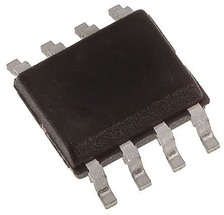
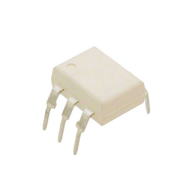
| 描述 | IC OPAMP VFB 120MHZ RRO 8SOIC高速运算放大器 Low-Distortion High- Speed R-to-R Output |
| 产品分类 | Linear - Amplifiers - Instrumentation, OP Amps, Buffer Amps集成电路 - IC |
| 品牌 | Texas Instruments |
| 产品手册 | |
| 产品图片 |
|
| rohs | 符合RoHS无铅 / 符合限制有害物质指令(RoHS)规范要求 |
| 产品系列 | 放大器 IC,高速运算放大器,Texas Instruments THS4222D- |
| 数据手册 | |
| 产品型号 | THS4222D |
| 产品 | Voltage Feedback Amplifier |
| 产品目录页面 | |
| 产品种类 | |
| 供应商器件封装 | 8-SOIC |
| 共模抑制比—最小值 | 74 dB |
| 其它名称 | 296-13822-5 |
| 包装 | 管件 |
| 单位重量 | 76 mg |
| 压摆率 | 990 V/µs |
| 商标 | Texas Instruments |
| 增益带宽生成 | 120 MHz |
| 增益带宽积 | 120MHz |
| 安装类型 | 表面贴装 |
| 安装风格 | SMD/SMT |
| 封装 | Tube |
| 封装/外壳 | 8-SOIC(0.154",3.90mm 宽) |
| 封装/箱体 | SOIC-8 |
| 工作温度 | -40°C ~ 85°C |
| 工作电源电压 | 15 V |
| 工厂包装数量 | 75 |
| 拓扑结构 | Voltage Feedback |
| 放大器类型 | 电压反馈 |
| 最大功率耗散 | 1020 mW |
| 最大工作温度 | + 85 C |
| 最小工作温度 | - 40 C |
| 标准包装 | 75 |
| 电压-电源,单/双 (±) | 2.7 V ~ 15 V, ±1.35 V ~ 7.5 V |
| 电压-输入失调 | 3mV |
| 电压增益dB | 100 dB |
| 电流-电源 | 14mA |
| 电流-输入偏置 | 900nA |
| 电流-输出/通道 | 100mA |
| 电源电压-最大 | 15 V |
| 电源电压-最小 | 2.7 V |
| 电源电流 | 36 mA |
| 电路数 | 2 |
| 系列 | THS4222 |
| 设计资源 | http://www.digikey.com/product-highlights/cn/zh/texas-instruments-webench-design-center/3176 |
| 转换速度 | 550 V/us |
| 输入补偿电压 | 10 mV |
| 输出类型 | 满摆幅 |
| 通道数量 | 2 Channel |
| 配用 | /product-detail/zh/THS4222EVM/296-20552-ND/562166/product-detail/zh/THS4221EVM/296-18848-ND/863681 |


- 商务部:美国ITC正式对集成电路等产品启动337调查
- 曝三星4nm工艺存在良率问题 高通将骁龙8 Gen1或转产台积电
- 太阳诱电将投资9.5亿元在常州建新厂生产MLCC 预计2023年完工
- 英特尔发布欧洲新工厂建设计划 深化IDM 2.0 战略
- 台积电先进制程称霸业界 有大客户加持明年业绩稳了
- 达到5530亿美元!SIA预计今年全球半导体销售额将创下新高
- 英特尔拟将自动驾驶子公司Mobileye上市 估值或超500亿美元
- 三星加码芯片和SET,合并消费电子和移动部门,撤换高东真等 CEO
- 三星电子宣布重大人事变动 还合并消费电子和移动部门
- 海关总署:前11个月进口集成电路产品价值2.52万亿元 增长14.8%


PDF Datasheet 数据手册内容提取
THS4221, THS4225 D−8 DBV−5 DGQ−10 DGN−8 DGK−8 THS4222, THS4226 www.ti.com SLOS399G − AUGUST 2002 − REVISED JANUARY 2004 LOW-DISTORTION, HIGH-SPEED, RAIL-TO-RAIL OUTPUT OPERATIONAL AMPLIFIERS FEATURES APPLICATIONS (cid:1) Low-Voltage Analog-to-Digital Converter (cid:1) Rail-to-Rail Output Swing Preamplifier − VO = −4.8/4.8 (RL = 2 kΩ) (cid:1) Active Filtering (cid:1) (cid:1) Video Applications High Speed − 230 MHz Bandwidth (−3 dB, G= 1) − 975 V/µs Slew Rate THS4222 D, DGN, OR DGK PACKAGE (cid:1) (TOP VIEW) Ultra-Low Distortion − HD2 = −90 dBc (f = 5 MHz, RL = 499Ω) 1OUT 1 8 VS+ − HD3 = −100 dBc (f = 5 MHz, RL = 499Ω) 1IN− 2 7 2OUT (cid:1) 1IN+ 3 6 2IN− High Output Drive, I = 100 mA (typ) O VS− 4 5 2IN+ (cid:1) Excellent Video Performance − 40 MHz Bandwidth (0.1 dB, G = 2) − 0.007% Differential Gain − 0.007° Differential Phase RELATED DEVICES (cid:1) DEVICE DESCRIPTION Wide Range of Power Supplies − V = 3 V to 15 V THS4211 1 GHz, 800 V/µs, Vn = 7 nV/√Hz S THS4271 1.4 GHz, 900 V/µs, Vn = 3 nV/√Hz (cid:1) Power-Down Mode (THS4225/6) OPA354 250 MHz, 150 V/µs, Vn = 6.5 nV/√Hz (cid:1) Evaluation Module Available OPA690 500 MHz, 1800 V/µs, Vn = 5.5 nV/√Hz DESCRIPTION The THS4222 family is a set of rail-to-rail output single, and dual low-voltage, high-output swing, low-distortion high-speed amplifiers ideal for driving data converters, video switching or low distortion applications.This family of voltage feedback amplifiers can operate from a single 15-V power supply down to a single 3-V power supply while consuming only 14 mA of quiescent current per channel. In addition, the family offers excellent ac performance with 230-MHz bandwidth, 975-V/µs slew rate and harmonic distortion (THD) at –90 dBc at 5 MHz. SLEW RATE vs DIFFERENTIAL DRIVE CIRCUIT DIFFERENTIAL OUTPUT VOLTAGE STEP 1.3 kΩ 1800 5 V 1600 Fall 650 Ω 0.1 µF 10 µF s 1400 IN+ µ − V/ Vout− e − 1200 Rise 2.5 V + Rat 1000 w e 800 1.3 kΩ 1 kΩ R − Sl 600 650 Ω S IN− 400 − Vout+ 200 2.5 V + 0 0 1 2 3 4 5 6 7 8 9 10 THS4222 VO − Differential Output Voltage Step − V Please be aware that an important notice concerning availability, standard warranty, and use in critical applications of TexasInstruments semiconductor products and disclaimers thereto appears at the end of this data sheet. PRODUCTION DATA information is current as of publication date. Products Copyright © 2002 − 2004, Texas Instruments Incorporated conform to specifications per the terms of Texas Instruments standard warranty. Production processing does not necessarily include testing of all parameters.
THS4221, THS4225 THS4222, THS4226 www.ti.com SLOS399G − AUGUST 2002 − REVISED JANUARY 2004 This integrated circuit can be damaged by ESD. Texas ABSOLUTE MAXIMUM RATINGS Instruments recommends that all integrated circuits be over operating free-air temperature range unless otherwise noted(1) handled with appropriate precautions. Failure to observe UNIT proper handling and installation procedures can cause damage. Supply voltage, VS 16.5 V Input voltage, VI ±VS ESD damage can range from subtle performance degradation to complete device failure. Precision integrated circuits may be more Output current, IO 100 mA susceptible to damage because very small parametric changes could Differential input voltage, VID 4 V cause the device not to meet its published specifications. Continuous power dissipation See Dissipation Rating Table Maximum junction temperature, TJ 150°C PACKAGE DISSIPATION RATINGS Mopaexriamtiuomn, jluonncgt itoenr mte rmepliaebrailtituyr eT,J c(2o)ntinuous 125°C PPAACCKKAAGGEE (°ΘΘCJJ/WCC) (ΘΘ°CJJAA/W((1))) TAP ≤O 2W5E°CR RATTAI N=G 8(52°)C Storage temperature range, Tstg −65°C to 150°C DBV (5) 55 255.4 391 mW 156 mW Lead temperature 300°C D (8) 38.3 97.5 1.02 W 410 mW 1,6 mm (1/16 inch) from case for 10 seconds DGN (8) (3) 4.7 58.4 1.71 W 685 mW THS4221/5 2500 V HHBBMM DGK (8) 54.2 260 385 mW 154 mW THS4222/6 3000 V DGQ (10) (3) 4.7 58 1.72 W 690 mW EESSDD rraattiinnggss:: CDM 1500 V (1) This data was taken using the JEDEC standard High-K test PCB. THS4221/5 150 V MMMM (2) Power rating is determined with a junction temperature of 125°C. THS4222/6 200 V This is the point where distortion starts to substantially increase. (1) The absolute maximum ratings under any condition is limited by Thermal management of the final PCB should strive to keep the the constraints of the silicon process. Stresses above these junction temperature at or below 125°C for best performance and ratings may cause permanent damage. Exposure to absolute long term reliability. maximum conditions for extended periods may degrade device (3) The THS422x may incorporate a PowerPAD on the underside of reliability. These are stress ratings only, and functional operation the chip. This acts as a heatsink and must be connected to a of the device at these or any other conditions beyond those thermally dissipative plane for proper power dissipation. Failure specified is not implied. to do so may result in exceeding the maximum junction (2) The maximum junction temperature for continuous operation is temperature which could permanently damage the device. See TI limited by package constraints. Operation above this temperature technical brief SLMA002 and SLMA004 for more information may result in reduced reliability and/or lifetime of the device. about utilizing the PowerPAD thermally enhanced package. RECOMMENDED OPERATING CONDITIONS MIN MAX UNIT Dual supply ±1.35 ±7.5 SSuuppppllyy vvoollttaaggee, ((VVSS+ aanndd VVSS−)) VV Single supply 2.7 15 Input common-mode voltage range VS− + 1.1 VS+ − 1.1 V THS4221 AND THS4225 SINGLE PACKAGE/ORDERING INFORMATION PACKAGED DEVICES PLASTIC MSOP(2) PLASTIC SMALL OUTLINE SOT-23(1) PowerPAD(cid:1) PLASTIC MSOP(2) ((DD)) (DBV) SYM (DGN) SYM (DGK) SYM THS4221D THS4221DBV BFS THS4221DGN BFT THS4221DGK BHX THS4225D — — THS4225DGN BFU THS4225DGK BFY (1) All packages are available taped and reeled. The R suffix standard quantity is 3000. The T suffix standard quantity is 250 (e.g., THS4221DBVT). (2) All packages are available taped and reeled. The R suffix standard quantity is 2500 (e.g., THS4221DGNR). PowerPAD is a trademark of Texas Instruments. 2
THS4221, THS4225 THS4222, THS4226 www.ti.com SLOS399G − AUGUST 2002 − REVISED JANUARY 2004 THS4222 AND THS4226 DUAL PACKAGE/ORDERING INFORMATION PACKAGED DEVICES PPLLAASSTTIICC SSMMAALLLL OOUUTTLLIINNEE PLASTIC MSOP PowerPAD(cid:1)(1) PLASTIC MSOP(cid:1)(1) (D)(1) (DGN) SYM (DGQ) SYM (DGK) SYM THS4222D THS4222DGN BFO — — THS4222DGK BHW — — — THS4226DGQ BFP — — (1) All packages are available taped and reeled. The R suffix standard quantity is 2500 (e.g., THS4222DGNR). ELECTRICAL CHARACTERISTICS VS = ±5 V, RL = 499 Ω, and G = 1 unless otherwise noted TYP OVER TEMPERATURE PARAMETER TEST CONDITIONS 25°C 25°C 07°0C° Cto −4805°°CC to UNITS MMAINX/ AC PERFORMANCE G = 1, PIN = −7 dBm 230 MHz Typ G = 2, PIN = −13 dBm, Rf = 1.3 kΩ 100 MHz Typ SSmmaallll ssiiggnnaall bbaannddwwiiddtthh G = 5, PIN = −21 dBm, Rf = 2 kΩ 25 MHz Typ G = 10, PIN = −27 dBm, Rf = 2 kΩ 12 MHz Typ 0.1 dB flat bandwidth G = 2, PIN = −13 dBm, Rf = 1.3 kΩ 40 MHz Typ Gain bandwidth product G > 10, f = 1 MHz, Rf = 2 kΩ 120 MHz Typ Full-power bandwidth G = 1, VO = ±2.5 V 65 MHz Typ G = −1, VO = ±2.5 Vpp 990 V/µs Min SSlleeww rraattee G = 1, VO = ±2.5 Vpp 975 V/µs Min Settling time to 0.1% G = −1, VO = ±2 Vpp 25 ns Typ Settling time to 0.01% G = −1, VO = ±2 Vpp 52 ns Typ Harmonic distortion G = 1, VO = 2 VPP, f = 5 MHz RL = 499 Ω −90 dBc Typ SSeeccoonndd hhaarrmmoonniicc ddiissttoorrttiioonn RL = 150 Ω −92 dBc Typ RL = 499 Ω −100 dBc Typ TThhiirrdd hhaarrmmoonniicc ddiissttoorrttiioonn RL = 150 Ω −96 dBc Typ Differential gain (NTSC, PAL) G = 2, R = 150 Ω 0.007 % Typ Differential phase (NTSC, PAL) G = 2, R = 150 Ω 0.007 ° Typ Input voltage noise f = 1 MHz 13 nV/√Hz Typ Input current noise f = 1 MHz 0.8 pA/√Hz Typ Crosstalk (dual only) f = 5 MHz Ch-to-Ch −90 dB Typ DC PERFORMANCE Open-loop voltage gain (AOL) VO = ±2 V 100 80 75 75 dB Min Input offset voltage VCM = 0 V 3 10 16 16 mV Max Average offset voltage drift VCM = 0 V ±20 ±20 µV/(cid:2)C Typ Input bias current VCM = 0 V 0.9 3 5 5 µA Max Average offset voltage drift VCM = 0 V ±10 ±10 µV/(cid:2)C Typ Input offset current VCM = 0 V 100 500 700 700 nA Max Average offset current drift VCM = 0 V ±10 ±10 nA/(cid:2)C Typ INPUT CHARACTERISTICS Common-mode input range −4 / 4 −3.9 / 3.9 V Min Common-mode rejection ratio VCM = ±2 V 94 74 69 69 dB Min Input resistance 33 MΩ Typ Input capacitance Common-mode / differential 1 / 0.5 pF Max 3
THS4221, THS4225 THS4222, THS4226 www.ti.com SLOS399G − AUGUST 2002 − REVISED JANUARY 2004 ELECTRICAL CHARACTERISTICS VS = ±5 V, RL = 499 Ω, and G = 1 unless otherwise noted TYP OVER TEMPERATURE PARAMETER TEST CONDITIONS 25°C 25°C 07°0C° Cto −4805°°CC to UNITS MMAINX/ OUTPUT CHARACTERISTICS −4.4 / OOuuttppuutt vvoollttaaggee sswwiinngg RL = 499 Ω −4.7 / 4.7 −4.5 / 4.5 4.4 −4.4 / 4.4 V Min RL = 2 kΩ −4.8 / 4.8 V Min Output current (sourcing) RL = 10 Ω 100 92 88 88 mA Min Output current (sinking) RL = 10 Ω −100 −92 −88 −88 mA Min Output impedance f = 1 MHz 0.02 Ω Typ POWER SUPPLY Specified operating voltage ±5 ±7.5 ±7.5 ±7.5 V Max Maximum quiescent current Per channel 14 18 20 22 mA Max Power supply rejection (±PSRR) 75 62 60 60 dB Min POWER-DOWN CHARACTERISTICS PD ≤ REF +1.0 V, REF = 0 V, Maximum power-down current 700 900 1000 1000 µA Max Per channel Enable REF+1.8 V Min RREEFF = 00 VV, oorr VVSS− Power down REF+1 V Max PPoowweerr-ddoowwnn vvoollttaaggee lleevveell((11)) Enable REF−1 V Min RREEFF = VVSS+ oorr ffllooaattiinngg Power down REF−1.5 V Max Turnon time delay 50% of final value 200 ns Typ Turnoff time delay 50% of final value 500 ns Typ Input impedance 58 Ω Typ Isolation f = 5 MHz 80 dB Typ (1) For detail information on the power-down circuit, refer to the powerdown section in the application information of this data sheet. 4
THS4221, THS4225 THS4222, THS4226 www.ti.com SLOS399G − AUGUST 2002 − REVISED JANUARY 2004 ELECTRICAL CHARACTERISTICS VS = 5 V, RL = 499 Ω, and G = 1 unless otherwise noted TYP OVER TEMPERATURE PARAMETER TEST CONDITIONS 25°C 25°C 07°0C° Cto −4805°°CC to UNITS MMAINX/ AC PERFORMANCE G = 1, PIN = −7 dBm 200 MHz Typ G = 2, PIN = −13 dBm, Rf = 1.3 kΩ 100 MHz Typ SSmmaallll ssiiggnnaall bbaannddwwiiddtthh G = 5, PIN = −21 dBm, Rf = 2 kΩ 25 MHz Typ G = 10, PIN = −27 dBm, Rf = 2 kΩ 12 MHz Typ 0.1 dB flat bandwidth G = 2, PIN = −13 dBm, Rf = 1.3 kΩ 50 MHz Typ Gain bandwidth product G > 10, f = 1 MHz, Rf = 2 kΩ 120 MHz Typ Full-power bandwidth G = 1, VO = ±2 V 40 MHz Typ G = −1, VO = ±2 Vpp 500 V/µs Min SSlleeww rraattee G = 1, VO = ±2 Vpp 550 V/µs Min Settling time to 0.1% G = −1, VO = ±1 Vpp 27 ns Typ Settling time to 0.01% G = −1, VO = ±1 Vpp 48 ns Typ Harmonic distortion G = 1, VO = 2 VPP, f = 5 MHz RL = 499 Ω −90 dBc Typ SSeeccoonndd hhaarrmmoonniicc ddiissttoorrttiioonn RL = 150 Ω −93 dBc Typ RL = 499 Ω −89 dBc Typ TThhiirrdd hhaarrmmoonniicc ddiissttoorrttiioonn RL = 150 Ω −91 dBc Typ Differential gain (NTSC, PAL) G = 2, R = 150 Ω 0.014 % Typ Differential phase (NTSC, PAL) G = 2, R = 150 Ω 0.011 ° Typ Input voltage noise f = 1 MHz 13 nV/√Hz Typ Input current noise f = 1 MHz 0.8 pA/√Hz Typ Crosstalk (dual only) f = 5 MHz Ch-to-Ch −90 dB Typ DC PERFORMANCE Open-loop voltage gain (AOL) VO = 1.5 V to 3.5 V 100 80 75 75 dB Min Input offset voltage VCM = 2.5 V 3 10 16 16 mV Max Average offset voltage drift VCM = 2.5 V ±20 ±20 µV/(cid:2)C Typ Input bias current VCM = 2.5 V 0.9 3 5 5 µA Max Average offset voltage drift VCM = 2.5 V ±10 ±10 µV/(cid:2)C Typ Input offset current VCM = 2.5 V 100 500 700 700 nA Max Average offset current drift VCM = 2.5 V ±10 ±10 nA/(cid:2)C Typ INPUT CHARACTERISTICS Common-mode input range 1 / 4 1.1 / 3.9 V Min Common-mode rejection ratio VCM = 1.5 V to 3.5 V 96 74 69 69 dB Min Input resistance 33 MΩ Typ Input capacitance Common-mode / differential 1 / 0.5 pF Max OUTPUT CHARACTERISTICS RL = 499 Ω 0.2 / 4.8 0.3 / 4.7 0.4 / 4.6 0.4 / 4.6 V Min OOuuttppuutt vvoollttaaggee sswwiinngg RL = 2 kΩ 0.1 / 4.9 V Min Output current (sourcing) RL = 10 Ω 95 85 80 80 mA Min Output current (sinking) RL = 10 Ω −95 −85 −80 −80 mA Min Output impedance f = 1 MHz 0.02 Ω Typ 5
THS4221, THS4225 THS4222, THS4226 www.ti.com SLOS399G − AUGUST 2002 − REVISED JANUARY 2004 ELECTRICAL CHARACTERISTICS (continued) VS = 5 V, RL = 499 Ω, and G = 1 unless otherwise noted TYP OVER TEMPERATURE PARAMETER TEST CONDITIONS 25°C 25°C 07°0C° Cto to−4 805°°CC UNITS MMAINX/ POWER SUPPLY Specified operating voltage 5 15 15 15 V Max Maximum quiescent current Per channel 12 15 17 19 mA Max Power supply rejection (±PSRR) 70 62 60 60 dB Min POWER-DOWN CHARACTERISTICS PD ≤ REF +1.0 V, REF = 0 V, Maximum power-down current 500 750 900 900 µA Max Per channel Enable REF+1.8 V Min RREEFF = 00 VV, oorr VVSS− Power down REF+1 V Max PPoowweerr-ddoowwnn vvoollttaaggee lleevveell((11)) Enable REF−1 V Min RREEFF = VVSS+ oorr ffllooaattiinngg Power down REF−1.5 V Max Turnon time delay 50% of final value 200 ns Typ Turnoff time delay 50% of final value 500 ns Typ Input impedance 58 Ω Typ Isolation f = 5 MHz 80 dB Typ (1) For detail information on the power-down circuit, refer to the powerdown section in the application information of this data sheet. 6
THS4221, THS4225 THS4222, THS4226 www.ti.com SLOS399G − AUGUST 2002 − REVISED JANUARY 2004 ELECTRICAL CHARACTERISTICS VS = 3.3 V, RL = 499 Ω, and G = 1 unless otherwise noted TYP OVER TEMPERATURE PARAMETER TEST CONDITIONS 25°C 25°C 07°0C° Cto −4805°°CC to UNITS MMAINX/ AC PERFORMANCE G = 1, PIN = −7 dBm 200 MHz Typ G = 2, PIN = −13 dBm, Rf = 1 kΩ 100 MHz Typ SSmmaallll ssiiggnnaall bbaannddwwiiddtthh G = 5, PIN = −21 dBm, Rf = 2 kΩ 15 MHz Typ G = 10, PIN = −27 dBm, Rf = 2 kΩ 12 MHz Typ 0.1 dB flat bandwidth G = 2, PIN = −13 dBm, Rf = 1 kΩ 50 MHz Typ Gain bandwidth product G > 10, f = 1 MHz, Rf = 1.5 kΩ 120 MHz Typ Full-power bandwidth G = 1, VO = 1.3 V to 2 V 50 MHz Typ G = −1, VO = 1.3 V to 2 V 120 V/µs Min SSlleeww rraattee G = 1, VO = 1.3 V to 2V 250 V/µs Min Harmonic distortion G = 2, VO = 1 VPP, f = 5 MHz RL = 499 Ω −80 dBc Typ SSeeccoonndd hhaarrmmoonniicc ddiissttoorrttiioonn RL = 150 Ω −79 dBc Typ RL = 499 Ω −91 dBc Typ TThhiirrdd hhaarrmmoonniicc ddiissttoorrttiioonn RL = 150 Ω −92 dBc Typ Input voltage noise f = 1 MHz 13 nV/√Hz Typ Input current noise f = 1 MHz 0.8 pA/√Hz Typ Crosstalk (dual only) f = 5 MHz Ch-to-Ch −90 dB Typ DC PERFORMANCE Open-loop voltage gain (AOL) VO = 1.35 V to 1.95 V 98 80 75 75 dB Min Input offset voltage VCM = 1.65 V 3 10 16 16 mV Max Average offset voltage drift VCM = 1.65 V ±20 ±20 µV/(cid:2)C Typ Input bias current VCM = 1.65 V 0.9 3 5 5 µA Max Average offset voltage drift VCM = 1.65 V ±10 ±10 µV/(cid:2)C Typ Input offset current VCM = 1.65 V 100 500 700 700 nA Max Average offset current drift VCM = 1.65 V ±10 ±10 nA/(cid:2)C Typ INPUT CHARACTERISTICS Common-mode input range 1 / 2.3 1.1/2.2 V Min Common-mode rejection ratio VCM = 1.35 V to 1.95 V 92 74 69 69 dB Min Input resistance 33 MΩ Typ Input capacitance Common-mode / differential 1 / 0.5 pF Max OUTPUT CHARACTERISTICS Output voltage swing RL = 499 Ω 0.15/3.15 0.3/3.0 0.35/2.95 0.35/2.95 V Min Output voltage swing RL = 2 kΩ 0.1 / 3.2 V Min Output current (sourcing) RL = 20 Ω 50 45 40 40 mA Min Output current (sinking) RL = 20 Ω −50 −45 −40 −40 mA Min Output impedance f = 1 MHz 0.02 Ω Typ 7
THS4221, THS4225 THS4222, THS4226 www.ti.com SLOS399G − AUGUST 2002 − REVISED JANUARY 2004 ELECTRICAL CHARACTERISTICS (continued) VS = 3.3 V, RL = 499 Ω, and G = 1 unless otherwise noted TYP OVER TEMPERATURE PARAMETER TEST CONDITIONS 25°C 25°C 07°0C° Cto to−4 805°°CC UNITS MMAINX/ POWER SUPPLY Specified operating voltage 3.3 15 15 15 V Max Maximum quiescent current Per channel 11 13 16 17 mA Max Power supply rejection (±PSRR) 65 60 55 55 dB Min POWER-DOWN CHARACTERISTICS PD ≤ REF +1.0 V, REF = 0 V, Maximum power-down current 500 700 800 800 µA Max Per channel Enable REF+1.8 V Min RREEFF = 00 VV, oorr VVSS− Power down REF+1 V Max PPoowweerr-ddoowwnn vvoollttaaggee lleevveell((11)) Enable REF−1 V Min RREEFF = VVSS+ oorr ffllooaattiinngg Power down REF−1.5 V Max Turnon time delay 50% of final value 200 ns Typ Turnoff time delay 50% of final value 500 ns Typ Input impedance 58 Ω Typ Isolation f = 5 MHz 80 dB Typ (1) For detail information on the power-down circuit, refer to the powerdown section in the application information of this data sheet. 8
THS4221, THS4225 THS4222, THS4226 www.ti.com SLOS399G − AUGUST 2002 − REVISED JANUARY 2004 PIN ASSIGNMENTS NON-POWER DOWN PACKAGE DEVICES THS4221 THS4221 THS4222 DBV PACKAGE D, DGN, OR DGK PACKAGE D, DGN, OR DGK PACKAGE (TOP VIEW) (TOP VIEW) (TOP VIEW) VOUT 1 5 VS+ NC 1 8 NC 1OUT 1 8 VS+ IN− 2 7 VS+ 1IN− 2 7 2OUT VS− 2 IN+ 3 6 VOUT 1IN+ 3 6 2IN− VS− 4 5 NC VS− 4 5 2IN+ IN+ 3 4 IN− NC − No internal connection POWER-DOWN PACKAGE DEVICES THS4225 THS4226 D, DGN, OR DGK PACKAGE DGQ PACKAGE (TOP VIEW) (TOP VIEW) REF 1 8 PD 1OUT 1 10 VS+ IN− 2 7 VS+ 1IN− 2 9 2OUT IN+ 3 6 VOUT 1IN+ 3 8 2IN− VS− 4 5 NC VS− 4 7 2IN+ 1PD 5 6 2PD NC − No internal connection 9
THS4221, THS4225 THS4222, THS4226 www.ti.com SLOS399G − AUGUST 2002 − REVISED JANUARY 2004 TYPICAL CHARACTERISTICS TABLE OF GRAPHS FIGURE Small signal frequency response 1 Slew rate vs Output voltage step 2, 3 Harmonic distortion vs Frequency 4, 5, 8, 9 Harmonic distortion vs Output voltage swing 6, 7 Voltage and current noise vs Frequency 10 Differential gain vs Number of loads 11, 13 Differential phase vs Number of loads 12, 14 Quiescent current vs Supply voltage 15 Output voltage vs Load resistance 16 Open-loop gain and phase vs Frequency 17 Open-loop gain vs Supply voltage 18 Rejection ratio vs Frequency 19 Rejection ratio vs Case temperature 20 Common-mode rejection ratio vs Input common-mode range 21, 22 Input offset voltage vs Case temperature 23 Input bias and offset current vs Case temperature 24, 25 Power-down quiescent current vs Supply voltage 26 Output impedance in power down vs Frequency 27 Crosstalk vs Frequency 28 SLEW RATE SLEW RATE vs vs SMALL SIGNAL FREQUENCY RESPONSE OUTPUT VOLTAGE STEP OUTPUT VOLTAGE STEP 22 1200 600 all Signal Gain − dB 11111202468068 GGGaaainiinn = == 1 520,, , R RRff f = == 2 12 .k 3kΩ ΩkΩ RPVOSL U==T 4± =95 9 −V 7Ω dBm µsR − Slew Rate − V/ 1046800000000 GRRVSLfa =i==n 14±=.953 19 Vk ΩΩ Fall Rise µsR − Slew Rate − V/ 234500000000 GRVRSLfa =i==n 14=±.953 −9 Vk1 ΩΩ Fall Rise Sm 4 S S 2 200 100 Gain = 1, Rf = 0 0 −2 0 0 0.1 1 10 100 1 k 0 1 2 3 4 5 0 0.5 1 1.5 2 f − Frequency − MHz VO − Output Voltage Step − V VO − Output Voltage Step − V Figure 1 Figure 2 Figure 3 10
THS4221, THS4225 THS4222, THS4226 www.ti.com SLOS399G − AUGUST 2002 − REVISED JANUARY 2004 HARMONIC DISTORTION HARMONIC DISTORTION HARMONIC DISTORTION vs vs vs FREQUENCY FREQUENCY OUTPUT VOLTAGE SWING 0 0 0 −10 Gain = 1 −10 Gain = 1 −10 Gain = 1 monic Distortion − dBc −−−−−−765432000000 RVVOSL === 1±255 V0 VP ΩP HD2 monic Distortion − dBc −−−−−−765432000000 RVVOSL === 4±295 V9 VP ΩP HD2 monic Distortion − dBc −−−−−−765432000000 HRf D=L 38=, M54 9HV9z Ω HanDd2 5, ±V5 V Har −80 Har −80 Har −80 −90 HD3 −90 HD3 −90 HD3, ±5 V −100 −100 −100 0.1 1 10 100 0.1 1 10 100 0 0.5 1 1.5 2 2.5 3 3.5 4 4.5 5 f − Frequency − MHz f − Frequency − MHz VO − Output Voltage Swing − V Figure 4 Figure 5 Figure 6 HARMONIC DISTORTION HARMONIC DISTORTION HARMONIC DISTORTION vs vs vs OUTPUT VOLTAGE SWING FREQUENCY FREQUENCY 0 0 0 Harmonic Distortion − dBc −−−−−−−−8765432100000000 GRfH=LaD 3 i=3n0 , 4=M59 1H9V zΩ HD3H,D ±25, V±5 V Harmonic Distortion − dBc −−−−−−−−8765432100000000 GRVVOSLa i==n= 1=525 V1V0P ΩP HD3 Harmonic Distortion − dBc −−−−−−−−8765432100000000 GRVVOSLa i==n= 4=529 V1V9P ΩP HD3 HD2 −90 HD2, 5 V −90 HD2 −90 −100 −100 −100 0 0.5 1 1.5 2 2.5 3 3.5 4 4.5 5 0.1 1 10 100 0.1 1 10 100 VO − Output Voltage Swing − V f − Frequency − MHz f − Frequency − MHz Figure 7 Figure 8 Figure 9 VOLTAGE AND CURRENT NOISE DIFFERENTIAL GAIN DIFFERENTIAL PHASE vs vs vs FREQUENCY NUMBER OF LOADS NUMBER OF LOADS 100 10 0.20 0.4 Gain = 2 Gain = 2 − Voltage Noise −nV/HzVn10 VInn 1 − Current Noise −pA/HzIn Differential Gain − % 00000000........0001111146802468 R4WIR0fo E =Ir Rs R1tE .aC5 m− ak psNΩeVT S±S1 C=0 05 V VS = ±5 V °Differential Phase − 000...000123...555123 R4W0fo =IrRs 1tE .C5 − ak sNΩeT S±1C00 IRE Ramp 0.05 0.02 1 0.1 0 0 1 k 10 k 100 k 1 M 10 M 0 1 2 3 4 5 0 1 2 3 4 5 f − Frequency − Hz Number of Loads − 150 Ω Number of Loads − 150 Ω Figure 10 Figure 11 Figure 12 11
THS4221, THS4225 THS4222, THS4226 www.ti.com SLOS399G − AUGUST 2002 − REVISED JANUARY 2004 DIFFERENTIAL GAIN DIFFERENTIAL PHASE QUIESCENT CURRENT vs vs vs NUMBER OF LOADS NUMBER OF LOADS SUPPLY VOLTAGE 0.20 0.4 22 Gain = 2 − % 000...111468 R4W0fo =IrRs 1tE .C5 − ak sPΩeA L±100 IRE Ramp °e − 0.03.53 GR4W0fao =iIrnRs 1tE= .C5 2− ak sPΩeA L±100 IRE Ramp mA/Ch 112680 TA = 85°C TA = 25°C Differential Gain 00000.....0001146802 VS = 5 V VS = ±5 V Differential Phas 00..0012..5512 Quiescent Current − 111024468 TA = −40°C 0.02 0.05 2 0 0 1 2 3 4 5 0 0 0 1 2 3 4 5 1.5 2 2.5 3 3.5 4 4.5 5 Number of Loads − 150 Ω Number of Loads − 150 Ω VS − Supply Voltage − ±V Figure 13 Figure 14 Figure 15 OUTPUT VOLTAGE OPEN-LOOP GAIN AND FHASE OPEN-LOOP GAIN vs vs vs LOAD RESISTANCE FREQUENCY SUPPLY VOLTAGE 5 110 220 105 4 100 VS = ±5 V, 5 V, 200 TA = 25°C V 3 90 and 3.3 V 180 − Output Voltage − VO −−01221 TA = −40 to 85°C pen-Loop Gain − dB345678000000 6811110002460000°Phase − Open-Loop Gain − dB 10905 O20 40 −3 10 20 −4 0 0 −5 −10 −20 90 10 100 1 k 10 k 0.0001 0.001 0.01 0.1 1 10 100 1000 1.5 2 2.5 3 3.5 4 4.5 5 RL − Load Resistance − Ω f − Frequency − MHz VS − Supply Voltage − ±V Figure 16 Figure 17 Figure 18 REJECTION RATIO REJECTION RATIO COMMON-MODE REJECTION RATIO vs vs vs FREQUENCY CASE TEMPERATURE INPUT COMMON-MODE RANGE 100 100 B 100 90 VS = ±5 V, 5 V, and 3.3 V VS = ±5 V, 5 V, and 3.3 V o − d 90 80 90 CMMR Rati 80 Rejection Ratios − dB 3456700000 PSRR CMMR Rejection Ratio − dB 678000 PSRR mmon-Mode Rejection 3456700000 1200 50 R − Co 1200 VTAS == 255 V°C R M 0 40 C 0 0.1 1 10 100 −40−30−20−10 0 102030405060708090 0 0.5 1 1.5 2 2.5 3 3.5 4 4.5 5 f − Frequency − MHz TC − Case Temperature − °C VICR − Input Common-Mode Voltage Range − V Figure 19 Figure 20 Figure 21 12
THS4221, THS4225 THS4222, THS4226 www.ti.com SLOS399G − AUGUST 2002 − REVISED JANUARY 2004 COMMON-MODE REJECTION RATIO INPUT OFFSET VOLTAGE vs vs INPUT COMMON-MODE RANGE CASE TEMPERATURE dB 100 4 ode Rejection Ratio − 5678900000 set Voltage − mV 23..5523 VS = 5 V mon-M 3400 put Off 1.5 m n RR − Co 1200 VTAS == 2±55° CV − IVOS 0.51 VS = ±5 V CM 0 0 −6 −4 −2 0 2 4 6 −40−30−20−10 0 102030405060708090 VICR − Input Common-Mode Voltage Range − V Case Temperature − °C Figure 22 Figure 23 INPUT BIAS AND OFFSET CURRENT INPUT BIAS AND OFFSET CURRENT vs vs CASE TEMPERATURE CASE TEMPERATURE 0.84 10 0.9 5 VS = 5 V VS = ±5 V 0.82 5 A 0.88 0 A µ− Input Bias Current −AIIB 0000....07777.24688 IOS IIB+ IIB− −−−−02115050µ− Input Offset Current −IOS µ− Input Bias Current −AIIB0000....07888.82468 IOS IIB− IIB+ −−−−−221155050 µ− Input Offset Current −IOS 0.7 −25 0.76 −30 −40−30−20−100 102030405060708090 −40−30−20−10 0 102030405060708090 Case Temperature − °C Case Temperature − °C Figure 24 Figure 25 POWER-DOWN QUIESCENT CURRENT OUTPUT IMPEDANCE IN POWER DOWN CROSSTALK vs vs vs SUPPLY VOLTAGE FREQUENCY FREQUENCY h1000 3200 120 µA/C 900 2800 GRLa i=n 4=9 29 Ω er-Down Quiescent Current − 234567800000000000000 TA = 85°C TA T=A − =4 02°5C°C Ω− Output Impedance −RO1122260480000000000 RPVISfN = == 1 ±.155 dVkBΩm Crosstalk − dB 10246800000 VGRVTASILaN i====n 24−±=5951 1°9 CVd ΩB, 5 V, and 3.3 VPalDl C Chraonsnsetalslk Pow 100 400 Crosstalk all Channels 01.5 2 2.5 3 3.5 4 4.5 5 00.1 1 10 100 1 k 00.1 1 10 100 1 k VS − Supply Voltage − ±V f − Frequency − MHz f − Frequency − MHz Figure 26 Figure 27 Figure 28 13
THS4221, THS4225 THS4222, THS4226 www.ti.com SLOS399G − AUGUST 2002 − REVISED JANUARY 2004 APPLICATION INFORMATION HIGH-SPEED OPERATIONAL AMPLIFIERS 5 V +VS The THS4222 family of operational amplifiers is a family of + single and dual, rail-to-rail output voltage feedback amplifiers. The THS4222 family combines both a high 50 Ω Source 100 pF 0.1 µF 6.8 µF slew rate and a rail-to-rail output stage. + VI The THS4225 and THS4226 provides a power-down 49.9 Ω _THS4222 VO mode, providing the ability to save power when the 499 Ω Rf amplifier is inactive. A reference pin is provided to allow the user the flexibility to control the threshold levels of the 1.3 kΩ Rg 1.3 kΩ power-down control pin. 0.1 µF 6.8 µF 100 pF + Applications Section Contents (cid:1) −VS Wideband, Noninverting Operation −5 V (cid:1) Wideband, Inverting Gain Operation (cid:1) Single Supply Operation (cid:1) Figure 29. Wideband, Noninverting Gain Saving Power With Power-Down Functionality and Configuration Setting Threshold Levels With the Reference Pin (cid:1) Power Supply Decoupling Techniques and Recommendations (cid:1) Driving an ADC With the THS4222 WIDEBAND, INVERTING OPERATION (cid:1) Active Filtering With the THS4222 (cid:1) An Abbreviated Analysis of Noise in Amplifiers Since the THS4222 family are general-purpose, wideband (cid:1) Driving Capacitive Loads voltage-feedback amplifiers, several familiar operational (cid:1) Printed Circuit Board Layout Techniques for Optimal amplifier applications circuits are available to the designer. Figure 30 shows a typical inverting configuration where Performance (cid:1) the input and output impedances and noise gain from Power Dissipation and Thermal Considerations (cid:1) Figure 29 are retained in an inverting circuit configuration. Evaluation Fixtures, Spice Models, and Applications Inverting operation is one of the more common Support (cid:1) requirements and offers several performance benefits. Additional Reference Material (cid:1) The inverting configuration shows improved slew rates Mechanical Package Drawings and distortion due to the pseudo-static voltage maintained on the inverting input. 5 V WIDEBAND, NONINVERTING OPERATION +VS + The THS4222 is a family of unity gain stable rail-to-rail output voltage feedback operational amplifiers, with and 100 pF 0.1 µF 6.8 µF without power-down capability, designed to operate from + a single 3-V to 15-V power supply. 0.1 CµFT R64T9 Ω T_HS4222 VO Figure 29 is the noninverting gain configuration of 2 V/V 499 Ω used to demonstrate the typical performance curves. 50 Ω Source Rg Rf Voltage feedback amplifiers, unlike current feedback VI 1.3 kΩ 1.3 kΩ designs, can use a wide range of resistors values to set R52M.3 Ω 0.1 µF 6.8 µF their gain with minimal impact on their stability and 100 pF + frequency response. Larger-valued resistors decrease the loading effect of the feedback network on the output of the amplifier, but this enhancement comes at the expense of −5 V−VS additional noise and potentially lower bandwidth. Feedback resistor values between 1 kΩ and 2 kΩ are Figure 30. Wideband, Inverting Gain recommended for most situations. Configuration 14
THS4221, THS4225 THS4222, THS4226 www.ti.com SLOS399G − AUGUST 2002 − REVISED JANUARY 2004 In the inverting configuration, some key design +VS considerations must be noted. One is that the gain resistor 50 Ω Source (R ) becomes part of the signal channel input impedance. g + If the input impedance matching is desired (which is beneficial whenever the signal is coupled through a cable, VI RT 49.9 Ω _THS4222 VO twisted pair, long PC board trace, or other transmission 499 Ω ltienrem icnoantidounc vtoarlsu)e, aRngd mRfa ayd jbues tesde tt oe gqiuvael thtoe dthees irreedq ugiareind. +V2S Rf However, care must be taken when dealing with low Rg 1.3 kΩ inverting gains, as the resultant feedback resistor value 1.3 kΩ can present a significant load to the amplifier output. For an inverting gain of 2, setting R to 49.9 Ω for input +VS g matching eliminates the need for RM but requires a 100-Ω 2 Rf feedback resistor. This has an advantage of the noise gain 1.3 kΩ becoming equal to 2 for a 50-Ω source impedance—the VS 50 Ω Source same as the noninverting circuit in Figure 29. However, the Rg _ amplifier output now sees the 100-Ω feedback resistor in parallel with the external load. To eliminate this excessive VI52.3 Ω R1T.3 kΩ +THS4222 VO loading, it is preferable to increase both Rg and Rf, values, 499 Ω as shown in Figure 30, and then achieve the input +VS +VS matching impedance with a third resistor (RM) to ground. 2 2 The total input impedance becomes the parallel Figure 31. DC-Coupled Single Supply Operation combination of R and R . g M Saving Power With Power-Down Functionality The last major consideration to discuss in inverting and Setting Threshold Levels With the Reference amplifier design is setting the bias current cancellation Pin resistor on the noninverting input. If the resistance is set The THS4225 and THS4226 feature a power-down pin equal to the total dc resistance looking out of the inverting (PD) which lowers the quiescent current from 14 mA/ch terminal, the output dc error, due to the input bias currents, down to 700 µA/ch, ideal for reducing system power. is reduced to (input offset current) multiplied by R in f The power-down pin of the amplifiers defaults to the Figure 30, the dc source impedance looking out of the positive supply voltage in the absence of an applied inverting terminal is 1.3 kΩ || (1.3 kΩ + 25.6 Ω) = 649 Ω. voltage, putting the amplifier in the power-on mode of To reduce the additional high-frequency noise introduced operation. To turn off the amplifier in an effort to conserve by the resistor at the noninverting input, and power-supply power, the power-down pin can be driven towards the feedback, R is bypassed with a capacitor to ground. T negative rail. The threshold voltages for power-on and SINGLE SUPPLY OPERATION power-down are relative to the supply rails and given in the specification tables. Above the Enable Threshold Voltage, The THS4222 is designed to operate from a single 3-V to the device is on. Below the Disable Threshold Voltage, the 15-V power supply. When operating from a single power device is off. Behavior in between these threshold voltages supply, care must be taken to ensure the input signal and is not specified. amplifier are biased appropriately to allow for the Note that this power-down functionality is just that; the maximum output voltage swing. The circuits shown in amplifier consumes less power in power-down mode. The Figure 31 demonstrate methods to configure an amplifier power-down mode is not intended to provide a high- in a manner conducive for single supply operation. impedance output. In other words, the power-down functionality is not intended to allow use as a 3-state bus driver. When in power-down mode, the impedance looking back into the output of the amplifier is dominated by the feedback and gain setting resistors, but the output impedance of the device itself varies depending on the voltage applied to the outputs. The time delays associated with turning the device on and off are specified as the time it takes for the amplifier to reach 50% of the nominal quiescent current. The time delays are on the order of microseconds because the amplifier moves in and out of the linear mode of operation in these transitions. 15
THS4221, THS4225 THS4222, THS4226 www.ti.com SLOS399G − AUGUST 2002 − REVISED JANUARY 2004 Power-Down Reference Pin Operation In the above table, the threshold levels are derived by the following equations: In addition to the power-down pin, the THS4225 features REF − 1 V for enable a reference pin (REF) which allows the user to control the REF − 1.5 V for disable enable or disable power-down voltage levels applied to the Note that in order to maintain these threshold levels, the PD pin. Operation of the reference pin as it relates to the reference pin can be any voltage between (Vs+/2) + 1 V to power-down pin is described below. Vs+ or left floating. The reference pin is internally In most split-supply applications, the reference pin is connected to the positive rail, therefore it can be left connected to ground. In some cases, the user may want floating to maintain these threshold levels. to connect it to the negative or positive supply rail. In either For 3.3-V operation, the reference pin must be connected case, the user needs to be aware of the voltage level to the positive rail or left floating. thresholds that apply to the power-down pin. The tables below show examples and illustrate the relationship between the reference voltage and the power-down The recommended mode of operation is to tie the thresholds. reference pin to midrail, thus setting the threshold levels to midrail +1.0 V and midrail +1.8 V. POWER-DOWN THRESHOLD VOLTAGE LEVELS (REF ≤ Midrail) SUPPLY NO. OF CHANNELS PACKAGES RREEFFEERREENNCCEE PPIINN EENNAABBLLEE DDIISSAABBLLEE VVOOLLTTAAGGEE VOLTAGE (V) LEVEL (V) LEVEL (V) Single (8-pin) THS4225D, THS4225DGN (V) GND ≥ 1.8 ≤ 1 Power Supply Decoupling Techniques and ±±55 −2.5 ≥ −0.7 ≤ −1.5 Recommendations −5 ≥ −3.2 ≤ −4 GND ≥ 1.8 ≤1 Power supply decoupling is a critical aspect of any 55 1 ≥ 2.8 ≤2 high-performance amplifier design process. Careful 2.5 ≥ 4.3 ≤3.5 decoupling provides higher quality ac performance (most 3.3 GND ≥ 1.8 ≤1 notably improved distortion performance). The following guidelines ensure the highest level of performance. In the above table, the threshold levels are derived by the following equations: 1. Place decoupling capacitors as close to the power REF + 1.8 V for enable supply inputs as possible, with the goal of minimizing REF + 1 V for disable the inductance of the path from ground to the power Note that in order to maintain these threshold levels, the supply. reference pin can be any voltage between Vs− or GND up to Vs/2 (mid rail). 2. Placement priority should put the smallest valued For 3.3-V operation, the reference pin must be connected capacitors closest to the device. to the most negative rail (for single supply this is GND). POWER-DOWN THRESHOLD VOLTAGE LEVELS (REF > Midrail) 3. Use of solid power and ground planes is recommended to reduce the inductance along power SUPPLY RREEFFEERREENNCCEE PPIINN EENNAABBLLEE DDIISSAABBLLEE VVOOLLTTAAGGEE supply return current paths, with the exception of the VOLTAGE (V) LEVEL (V) LEVEL (V) (V) areas underneath the input and output pins. Floating or 5 ≥ 4 ≤ 3.5 ±±55 2.5 ≥ 1.5 ≤ 1 4. Recommended values for power supply decoupling 1 ≥ 0 ≤ −0.5 include a bulk decoupling capacitor (6.8 to 22 µF), a mid-range decoupling capacitor (0.1 µF) and a high Floating or 5 ≥ 4 ≤3.5 frequency decoupling capacitor (1000 pF) for each 55 4 ≥ 3 ≤2.5 supply. A 100 pF capacitor can be used across the 3.5 ≥ 2.5 ≤2 supplies as well for extremely high frequency return 3.3 Floating or 3.3 ≥ 2.7 ≤1.8 currents, but often is not required. 16
THS4221, THS4225 THS4222, THS4226 www.ti.com SLOS399G − AUGUST 2002 − REVISED JANUARY 2004 APPLICATION CIRCUITS performance can sometimes be achieved with single-ended input drive. An example circuit is shown here Driving an Analog-to-Digital Converter With the for reference. THS4222 50 Ω +5 V The THS4222 can be used to drive high-performance Source analog-to-digital converters. Two example circuits are presented below. VI + RISO 0.1 µF 49.9 Ω RT T_HS4222 16.5 Ω 68 pf INADS807 The first circuit uses a wideband transformer to convert a 12-Bit, single-ended input signal into a differential signal. The CM 53 Msps differential signal is then amplified and filtered by two −5 V Rf IN 1.82 kΩ THS4222 amplifiers. This circuit provides low 1.3 kΩ 0.1 µF intermodulation distortion, suppressed even-order Rg 1.3 kΩ distortion, 14 dB of voltage gain, a 50-Ω input impedance, and a single-pole filter at 25 MHz. For applications without signal content at dc, this method of driving ADCs can be NOTE: For best performance, high-speed ADCs should be driven very useful. Where dc information content is required, the differentially. See the THS4500 family of devices for more THS4500 family of fully differential amplifiers may be information. applicable. Figure 33. Driving an ADC With a Single-Ended Input 5 V + Active Filtering With the THS4222 THS4222 _ High-frequency active filtering with the THS4222 is achievable due to the amplifier’s high slew rate, wide 50 Ω (1:4 Ω) Source 1:2 −5 V bandwidth, and voltage feedback architecture. Several 649 Ω 1.3 kΩ 24.9 Ω options are available for high-pass, low-pass, bandpass, and bandstop filters of varying orders. A simple two-pole ADS807 low pass filter is presented here as an example, with two 4.7 pF 237 Ω 12-Bit, 53 Msps poles at about 25 MHz. 4.7 pF 649 Ω 24.9 Ω 1.3 kΩ 4.7 pF 50 Ω Source 1.3 kΩ _ THS4222 VI 1.3 kΩ 5 V + 52.3 Ω _ 49.9 Ω THS4222 VO + Figure 32. A Linear, Low Noise, High Gain ADC 120 pF Preamplifier −5 V The second circuit depicts single-ended ADC drive. While not recommended for optimum performance using Figure 34. A Two-Pole Active Filter With Two converters with differential inputs, satisfactory Poles at about 25 MHz 17
THS4221, THS4225 THS4222, THS4226 www.ti.com SLOS399G − AUGUST 2002 − REVISED JANUARY 2004 NOISE ANALYSIS distortion, the simplest and most effective solution is to isolate the capacitive load from the feedback loop by High slew rates, stable unity gain, voltage-feedback inserting a series isolation resistor between the amplifier operational amplifiers usually achieve their slew rate at the output and the capacitive load. This does not eliminate the expense of a higher input noise voltage. The input-referred pole from the loop response, but rather shifts it and adds voltage noise, and the two input-referred current noise a zero at a higher frequency. The additional zero acts to terms, combine to give low output noise under a wide cancel the phase lag from the capacitive load pole, thus variety of operating conditions. Figure 35 shows the increasing the phase margin and improving stability. amplifier noise analysis model with all the noise terms included. In this model, all noise terms are taken to be noise voltage or current density terms in either nV/√Hz or BOARD LAYOUT pA/√Hz. Achieving optimum performance with a high frequency ENI THS4222 FAMILY amplifier like the THS4222 requires careful attention to board layout parasitics and external component types. + EO Recommendations that optimize performance include: RS IBN _ 1. Minimize parasitic capacitance to any ac ground ERS 4kTRS Rf ERF fthoer alol uotfp tuhte asingdn ailn Iv/Oe rptiinngs . iPnapruats itpicin csa pcaacnita nccaeu osen instability: on the noninverting input, it can react with 4kT Rg IBI 4kTRf the source impedance to cause unintentional band Rg limiting. To reduce unwanted capacitance, a window 4kT = 1.6E−20J around the signal I/O pins should be opened in all of at 290K the ground and power planes around those pins. Otherwise, ground and power planes should be Figure 35. Noise Analysis Model unbroken elsewhere on the board. 2. Minimize the distance (< 0.25”) from the power The total output shot noise voltage can be computed as the supply pins to high frequency 0.1-µF decoupling square of all squares output noise voltage contributors. capacitors. At the device pins, the ground and power Equation 1 shows the general form for the output noise plane layout should not be in close proximity to the voltage using the terms shown in Figure 35: signal I/O pins. Avoid narrow power and ground tra(1ce)s (cid:5) (cid:2) (cid:4) to minimize inductance between the pins and the (cid:2) (cid:4)2 (cid:2) (cid:4)2 EO(cid:1) ENI2(cid:3) IBNRS (cid:3)4kTRS NG2(cid:3) IBIRf (cid:3)4kTRfNG decoupling capacitors. The power supply connections should always be decoupled with these capacitors. Dividing this expression by the noise gain (NG=(1+ R/R )) Larger (2.2-µF to 6.8-µF) decoupling capacitors, f g gives the equivalent input-referred spot noise voltage at effective at lower frequency, should also be used on the noninverting input, as shown in equation2: the main supply pins. These may be placed somewhat (cid:5) farther from the device and may be shared amo(n2g) (cid:2) (cid:4) 2 several devices in the same area of the PC board. E (cid:1) E 2(cid:3)(cid:2)I R (cid:4)2(cid:3)4kTR (cid:3) IBIRf (cid:3)4kTRf O NI BN S S NG NG 3. Careful selection and placement of external components will preserve the high frequency performance of the THS4222. Resistors should be Driving Capacitive Loads a very low reactance type. Surface-mount resistors One of the most demanding, and yet very common, load work best and allow a tighter overall layout. Metal-film conditions for an op amp is capacitive loading. Often, the and carbon composition, axially-leaded resistors can capacitive load is the input of an A/D converter, including also provide good high frequency performance. additional external capacitance, which may be Again, keep their leads and PC board trace length as recommended to improve A/D linearity. A high-speed, high short as possible. Never use wire wound type open-loop gain amplifier like the THS4222 can be very resistors in a high frequency application. Since the susceptible to decreased stability and closed-loop output pin and inverting input pin are the most response peaking when a capacitive load is placed directly sensitive to parasitic capacitance, always position the on the output pin. When the amplifier’s open-loop output feedback and series output resistor, if any, as close as resistance is considered, this capacitive load introduces possible to the output pin. Other network components, an additional pole in the signal path that can decrease the such as noninverting input termination resistors, phase margin. When the primary considerations are should also be placed close to the package. Where frequency response flatness, pulse response fidelity, or double-side component mounting is allowed, place 18
THS4221, THS4225 THS4222, THS4226 www.ti.com SLOS399G − AUGUST 2002 − REVISED JANUARY 2004 the feedback resistor directly under the package on the series resistor value as shown in the plot of R (ISO) the other side of the board between the output and vs Capacitive Load. This setting does not preserve inverting input pins. Even with a low parasitic signal integrity or a doubly-terminated line. If the input capacitance shunting the external resistors, impedance of the destination device is low, there is excessively high resistor values can create significant some signal attenuation due to the voltage divider time constants that can degrade performance. Good formed by the series output into the terminating axial metal-film or surface-mount resistors have impedance. approximately 0.2 pF in shunt with the resistor. For resistor values > 2.0 kΩ, this parasitic capacitance can 5. Socketing a high speed part like the THS4222 is not recommended. The additional lead length and add a pole and/or a zero below 400MHz that can pin-to-pin capacitance introduced by the socket can effect circuit operation. Keep resistor values as low as create a troublesome parasitic network which can possible, consistent with load driving considerations. make it almost impossible to achieve a smooth, stable It has been suggested here that a good starting point frequency response. Best results are obtained by for design would be set the R be set to 1.3 kΩ for f soldering the THS4222 onto the board. low-gain, noninverting applications. Doing this automatically keeps the resistor noise terms low, and PowerPAD™ DESIGN CONSIDERATIONS minimize the effect of their parasitic capacitance. The THS4222 family is available in a thermally-enhanced 4. Connections to other wideband devices on the PowerPAD family of packages. These packages are board may be made with short direct traces or constructed using a downset leadframe upon which the die through onboard transmission lines. For short is mounted [see Figure 36(a) and Figure 36(b)]. This connections, consider the trace and the input to the arrangement results in the lead frame being exposed as a next device as a lumped capacitive load. Relatively thermal pad on the underside of the package [see wide traces (50 mils to 100 mils) should be used, Figure 36(c)]. Because this thermal pad has direct thermal preferably with ground and power planes opened up contact with the die, excellent thermal performance can be around them. Estimate the total capacitive load and achieved by providing a good thermal path away from the set R from the plot of recommended R vs ISO ISO thermal pad. Capacitive Load. Low parasitic capacitive loads (<4pF) may not need an R , since the THS4222 The PowerPAD package allows for both assembly and (ISO) is nominally compensated to operate with a 2-pF thermal management in one manufacturing operation. parasitic load. Higher parasitic capacitive loads During the surface-mount solder operation (when the without an R are allowed as the signal gain (ISO) leads are being soldered), the thermal pad can also be increases (increasing the unloaded phase margin). If soldered to a copper area underneath the package. a long trace is required, and the 6-dB signal loss Through the use of thermal paths within this copper area, intrinsic to a doubly-terminated transmission line is heat can be conducted away from the package into either acceptable, implement a matched impedance a ground plane or other heat dissipating device. transmission line using microstrip or stripline techniques (consult an ECL design handbook for The PowerPAD package represents a breakthrough in microstrip and stripline layout techniques). A 50-Ω combining the small area and ease of assembly of surface environment is normally not necessary onboard, and mount with the heretofore awkward mechanical methods in fact a higher impedance environment improves of heatsinking. distortion as shown in the distortion versus load plots. With a characteristic board trace impedance defined DIE based on board material and trace dimensions, a Side View (a) Thermal matching series resistor into the trace from the output Pad of the THS4222 is used as well as a terminating shunt resistor at the input of the destination device. DIE Remember also that the terminating impedance is the End View (b) Bottom View (c) parallel combination of the shunt resistor and the input impedance of the destination device: this total Figure 36. Views of Thermally Enhanced effective impedance should be set to match the trace Package impedance. If the 6-dB attenuation of a doubly terminated transmission line is unacceptable, a long Although there are many ways to properly heatsink the trace can be series-terminated at the source end only. PowerPAD package, the following steps illustrate the Treat the trace as a capacitive load in this case and set recommended approach. 19
THS4221, THS4225 THS4222, THS4226 www.ti.com SLOS399G − AUGUST 2002 − REVISED JANUARY 2004 prevents solder from being pulled away from the 0.205 thermal pad area during the reflow process. 0.060 7. Apply solder paste to the exposed thermal pad area 0.017 and all of the IC terminals. Pin 1 0.013 8. With these preparatory steps in place, the IC is simply placed in position and run through the solder reflow 0.030 operation as any standard surface-mount 0.075 0.025 0.094 component. This results in a part that is properly installed. For a given θ , the maximum power dissipation is shown JA 0.035 0.040 0.010 in Figure 38 and is calculated by the equation 5: vias T (cid:6)T (3) Top View PD(cid:1) max(cid:1) A JA Figure 37. PowerPAD PCB Etch and Via where: Pattern PD = Maximum power dissipation of THS4222 (watts) TMAX = Absolute maximum junction temperature (150°C) PowerPAD PCB LAYOUT CONSIDERATIONS TθJAA = = F θrJeCe -+a mθCbAient temperature (°C) θJC = Thermal coefficient from junction to the case 1. Prepare the PCB with a top side etch pattern as shown θCA = Thermal coefficient from the case to ambient air in Figure 37. There should be etch for the leads as well (°C/W). as etch for the thermal pad. The next consideration is the package constraints. The 2. Place five holes in the area of the thermal pad. These two sources of heat within an amplifier are quiescent holes should be 13 mils in diameter. Keep them small power and output power. The designer should never forget so that solder wicking through the holes is not a about the quiescent heat generated within the device, problem during reflow. especially multi-amplifier devices. Because these devices have linear output stages (Class AB), most of the heat 3. Additional vias may be placed anywhere along the dissipation is at low output voltages with high output thermal plane outside of the thermal pad area. They currents. help dissipate the heat generated by the THS4222 family IC. These additional vias may be larger than the The other key factor when dealing with power dissipation 13-mil diameter vias directly under the thermal pad. is how the devices are mounted on the PCB. The They can be larger because they are not in the thermal PowerPAD devices are extremely useful for heat pad area to be soldered, so that wicking is not a dissipation. But, the device should always be soldered to problem. a copper plane to fully use the heat dissipation properties of the PowerPAD. The SOIC package, on the other hand, 4. Connect all holes to the internal ground plane. is highly dependent on how it is mounted on the PCB. As 5. When connecting these holes to the ground plane, do more trace and copper area is placed around the device, not use the typical web or spoke via connection θJA decreases and the heat dissipation capability methodology. Web connections have a high thermal increases. For a single package, the sum of the RMS resistance connection that is useful for slowing the output currents and voltages should be used to choose the heat transfer during soldering operations. This proper package. resistance makes the soldering of vias that have plane THERMAL ANALYSIS connections easier. In this application, however, low thermal resistance is desired for the most efficient The THS4222 family of devices does not incorporate heat transfer. Therefore, the holes under the THS4222 automatic thermal shutoff protection, so the designer must family PowerPAD package should make their take care to ensure that the design does not violate the connection to the internal ground plane, with a absolute maximum junction temperature of the device. complete connection around the entire circumference Failure may result if the absolute maximum junction of the plated-through hole. temperature of 150(cid:2) C is exceeded. 6. The top-side solder mask should leave the terminals The thermal characteristics of the device are dictated by of the package and the thermal pad area with its five the package and the PC board. Maximum power holes exposed. The bottom-side solder mask should dissipation for a given package can be calculated using the cover the five holes of the thermal pad area. This following formula. 20
THS4221, THS4225 THS4222, THS4226 www.ti.com SLOS399G − AUGUST 2002 − REVISED JANUARY 2004 T –T DESIGN TOOLS P (cid:1) max A Dmax (cid:1) JA Evaluation Fixtures, Spice Models, and where: Applications Support PDmax is the maximum power dissipation in the amplifier (W). Tmax is the absolute maximum junction temperature (°C). Texas Instruments is committed to providing its customers TA is the ambient temperature (°C). with the highest quality of applications support. To support θJA = θJC + θCA this goal, evaluation boards have been developed for the θcaJCs eis ( °thCe/W th)e.rmal coefficient from the silicon junctions to the THS4222 family of operational amplifiers. The boards are θCA is the thermal coefficient from the case to ambient air easy to use, allowing for straight-forward evaluation of the (°C/W). device. These evaluation boards can be ordered through the Texas Instruments web site, www.ti.com, or through your local Texas Instruments sales representative. For systems where heat dissipation is more critical, the Schematics for the two evaluation boards are shown THS4222 family is offered in MSOP with PowerPAD. The below with their default component values. Unpopulated thermal coefficient for the MSOP PowerPAD package is footprints are shown to provide insight into design substantially improved over the traditional SOIC. flexibility. Maximum power dissipation levels are depicted in the graph for the two packages. The data for the DGN R6 J2 package assumes a board layout that follows the R1 VS+ PowerPAD layout guidelines referenced above and detailed in the PowerPAD application notes in the R2 R6 J1 J3 Additional Reference Material section at the end of the U1:A data sheet. R4 R3 VS− PwrPad 3.5 W 8-Pin DGN Package − 3 n o pati 2.5 R7 Dissi 2 J4 R8 er w o 8-Pin D Package J6 P 1.5 R9 R11 m J5 u U1:B m xi 1 Ma R12 − 0.5 R10 D P 0 −40 −20 0 20 40 60 80 TA − Ambient Temperature − °C J7 J9 θθJJAA == 15780.4°°CC/W/W f foorr 8 8--PPinin S MOSICO P(D ()DGN) VS− GND TP1 VS+ ΤJ = 150°C, No Airflow Figure 38. Maximum Power Dissipation vs Ambient Temperature FB1 FB2 VS− VS+ When determining whether or not the device satisfies the + C6 C5 C9 C7 C8 C10 maximum power dissipation requirement, it is important to + consider not only quiescent power dissipation, but also dynamic power dissipation. Often maximum power dissipation is difficult to quantify because the signal pattern is inconsistent, but an estimate of the RMS power Figure 39. THS4222 EVM Circuit Configuration dissipation can provide visibility into a possible problem. 21
THS4221, THS4225 THS4222, THS4226 www.ti.com SLOS399G − AUGUST 2002 − REVISED JANUARY 2004 Figure 40. THS4222 EVM Board Figure 42. THS4222 EVM Board Layout Layout (Top Layer) (3rd Layer, Power) Figure 43. THS4222 EVM Board Layout Figure 41. THS4222 EVM Board Layout (Bottom Layer) (2nd Layer, Ground) 22
THS4221, THS4225 THS4222, THS4226 www.ti.com SLOS399G − AUGUST 2002 − REVISED JANUARY 2004 Computer simulation of circuit performance using SPICE amplifier, nor do they attempt to distinguish between the is often useful when analyzing the performance of analog package types in their small-signal ac performance. circuits and systems. This is particularly true for video and Detailed information about what is and is not modeled is RF amplifier circuits where parasitic capacitance and contained in the model file itself. inductance can have a major effect on circuit performance. A SPICE model for the THS4222 family is available through the Texas Instruments web site (www.ti.com). The ADDITIONAL REFERENCE MATERIAL PIC is also available for design assistance and detailed product information. These models do a good job of (cid:1) PowerPAD Made Easy, application brief (SLMA004) predicting small-signal ac and transient performance (cid:1) under a wide variety of operating conditions. They are not PowerPAD Thermally Enhanced Package, technical intended to model the distortion characteristics of the brief (SLMA002) 23
PACKAGE OPTION ADDENDUM www.ti.com 6-Feb-2020 PACKAGING INFORMATION Orderable Device Status Package Type Package Pins Package Eco Plan Lead/Ball Finish MSL Peak Temp Op Temp (°C) Device Marking Samples (1) Drawing Qty (2) (6) (3) (4/5) THS4221D ACTIVE SOIC D 8 75 Green (RoHS NIPDAU Level-1-260C-UNLIM -40 to 85 4221 & no Sb/Br) THS4221DBVR ACTIVE SOT-23 DBV 5 3000 Green (RoHS NIPDAU Level-1-260C-UNLIM -40 to 85 BFS & no Sb/Br) THS4221DBVT ACTIVE SOT-23 DBV 5 250 Green (RoHS NIPDAU Level-1-260C-UNLIM -40 to 85 BFS & no Sb/Br) THS4221DBVTG4 ACTIVE SOT-23 DBV 5 250 Green (RoHS NIPDAU Level-1-260C-UNLIM -40 to 85 BFS & no Sb/Br) THS4221DGK ACTIVE VSSOP DGK 8 80 Green (RoHS NIPDAU Level-1-260C-UNLIM -40 to 85 BHX & no Sb/Br) THS4221DGKR ACTIVE VSSOP DGK 8 2500 Green (RoHS NIPDAU Level-1-260C-UNLIM -40 to 85 BHX & no Sb/Br) THS4221DGN ACTIVE HVSSOP DGN 8 80 Green (RoHS NIPDAU Level-1-260C-UNLIM -40 to 85 BFT & no Sb/Br) THS4222D ACTIVE SOIC D 8 75 Green (RoHS NIPDAU Level-1-260C-UNLIM -40 to 85 4222 & no Sb/Br) THS4222DGK ACTIVE VSSOP DGK 8 80 Green (RoHS NIPDAU | NIPDAUAG Level-1-260C-UNLIM -40 to 85 BHW & no Sb/Br) THS4222DGN ACTIVE HVSSOP DGN 8 80 Green (RoHS NIPDAU | NIPDAUAG Level-1-260C-UNLIM -40 to 85 BFO & no Sb/Br) THS4222DGNR ACTIVE HVSSOP DGN 8 2500 Green (RoHS NIPDAU | NIPDAUAG Level-1-260C-UNLIM -40 to 85 BFO & no Sb/Br) THS4222DR ACTIVE SOIC D 8 2500 Green (RoHS NIPDAU Level-1-260C-UNLIM -40 to 85 4222 & no Sb/Br) THS4225D ACTIVE SOIC D 8 75 Green (RoHS NIPDAU Level-1-260C-UNLIM -40 to 85 4225 & no Sb/Br) THS4225DGK ACTIVE VSSOP DGK 8 80 Green (RoHS NIPDAU Level-1-260C-UNLIM -40 to 85 BFY & no Sb/Br) THS4225DGN ACTIVE HVSSOP DGN 8 80 Green (RoHS NIPDAU Level-1-260C-UNLIM -40 to 85 BFU & no Sb/Br) THS4226DGQ ACTIVE HVSSOP DGQ 10 80 Green (RoHS NIPDAU Level-1-260C-UNLIM -40 to 85 BFP & no Sb/Br) (1) The marketing status values are defined as follows: ACTIVE: Product device recommended for new designs. Addendum-Page 1
PACKAGE OPTION ADDENDUM www.ti.com 6-Feb-2020 LIFEBUY: TI has announced that the device will be discontinued, and a lifetime-buy period is in effect. NRND: Not recommended for new designs. Device is in production to support existing customers, but TI does not recommend using this part in a new design. PREVIEW: Device has been announced but is not in production. Samples may or may not be available. OBSOLETE: TI has discontinued the production of the device. (2) RoHS: TI defines "RoHS" to mean semiconductor products that are compliant with the current EU RoHS requirements for all 10 RoHS substances, including the requirement that RoHS substance do not exceed 0.1% by weight in homogeneous materials. Where designed to be soldered at high temperatures, "RoHS" products are suitable for use in specified lead-free processes. TI may reference these types of products as "Pb-Free". RoHS Exempt: TI defines "RoHS Exempt" to mean products that contain lead but are compliant with EU RoHS pursuant to a specific EU RoHS exemption. Green: TI defines "Green" to mean the content of Chlorine (Cl) and Bromine (Br) based flame retardants meet JS709B low halogen requirements of <=1000ppm threshold. Antimony trioxide based flame retardants must also meet the <=1000ppm threshold requirement. (3) MSL, Peak Temp. - The Moisture Sensitivity Level rating according to the JEDEC industry standard classifications, and peak solder temperature. (4) There may be additional marking, which relates to the logo, the lot trace code information, or the environmental category on the device. (5) Multiple Device Markings will be inside parentheses. Only one Device Marking contained in parentheses and separated by a "~" will appear on a device. If a line is indented then it is a continuation of the previous line and the two combined represent the entire Device Marking for that device. (6) Lead/Ball Finish - Orderable Devices may have multiple material finish options. Finish options are separated by a vertical ruled line. Lead/Ball Finish values may wrap to two lines if the finish value exceeds the maximum column width. Important Information and Disclaimer:The information provided on this page represents TI's knowledge and belief as of the date that it is provided. TI bases its knowledge and belief on information provided by third parties, and makes no representation or warranty as to the accuracy of such information. Efforts are underway to better integrate information from third parties. TI has taken and continues to take reasonable steps to provide representative and accurate information but may not have conducted destructive testing or chemical analysis on incoming materials and chemicals. TI and TI suppliers consider certain information to be proprietary, and thus CAS numbers and other limited information may not be available for release. In no event shall TI's liability arising out of such information exceed the total purchase price of the TI part(s) at issue in this document sold by TI to Customer on an annual basis. Addendum-Page 2
PACKAGE MATERIALS INFORMATION www.ti.com 6-Sep-2019 TAPE AND REEL INFORMATION *Alldimensionsarenominal Device Package Package Pins SPQ Reel Reel A0 B0 K0 P1 W Pin1 Type Drawing Diameter Width (mm) (mm) (mm) (mm) (mm) Quadrant (mm) W1(mm) THS4221DBVR SOT-23 DBV 5 3000 180.0 9.0 3.15 3.2 1.4 4.0 8.0 Q3 THS4221DBVT SOT-23 DBV 5 250 180.0 9.0 3.15 3.2 1.4 4.0 8.0 Q3 THS4221DGKR VSSOP DGK 8 2500 330.0 12.4 5.3 3.4 1.4 8.0 12.0 Q1 THS4222DGNR HVSSOP DGN 8 2500 330.0 12.4 5.3 3.4 1.4 8.0 12.0 Q1 THS4222DR SOIC D 8 2500 330.0 12.4 6.4 5.2 2.1 8.0 12.0 Q1 PackMaterials-Page1
PACKAGE MATERIALS INFORMATION www.ti.com 6-Sep-2019 *Alldimensionsarenominal Device PackageType PackageDrawing Pins SPQ Length(mm) Width(mm) Height(mm) THS4221DBVR SOT-23 DBV 5 3000 182.0 182.0 20.0 THS4221DBVT SOT-23 DBV 5 250 182.0 182.0 20.0 THS4221DGKR VSSOP DGK 8 2500 358.0 335.0 35.0 THS4222DGNR HVSSOP DGN 8 2500 364.0 364.0 27.0 THS4222DR SOIC D 8 2500 350.0 350.0 43.0 PackMaterials-Page2
PACKAGE OUTLINE DBV0005A SOT-23 - 1.45 mm max height SCALE 4.000 SMALL OUTLINE TRANSISTOR C 3.0 2.6 0.1 C 1.75 1.45 1.45 B A 0.90 PIN 1 INDEX AREA 1 5 2X 0.95 3.05 2.75 1.9 1.9 2 4 3 0.5 5X 0.3 0.15 0.2 C A B (1.1) TYP 0.00 0.25 GAGE PLANE 0.22 TYP 0.08 8 TYP 0.6 0 0.3 TYP SEATING PLANE 4214839/E 09/2019 NOTES: 1. All linear dimensions are in millimeters. Any dimensions in parenthesis are for reference only. Dimensioning and tolerancing per ASME Y14.5M. 2. This drawing is subject to change without notice. 3. Refernce JEDEC MO-178. 4. Body dimensions do not include mold flash, protrusions, or gate burrs. Mold flash, protrusions, or gate burrs shall not exceed 0.15 mm per side. www.ti.com
EXAMPLE BOARD LAYOUT DBV0005A SOT-23 - 1.45 mm max height SMALL OUTLINE TRANSISTOR PKG 5X (1.1) 1 5 5X (0.6) SYMM (1.9) 2 2X (0.95) 3 4 (R0.05) TYP (2.6) LAND PATTERN EXAMPLE EXPOSED METAL SHOWN SCALE:15X SOLDER MASK SOLDER MASK METAL UNDER METAL OPENING OPENING SOLDER MASK EXPOSED METAL EXPOSED METAL 0.07 MAX 0.07 MIN ARROUND ARROUND NON SOLDER MASK SOLDER MASK DEFINED DEFINED (PREFERRED) SOLDER MASK DETAILS 4214839/E 09/2019 NOTES: (continued) 5. Publication IPC-7351 may have alternate designs. 6. Solder mask tolerances between and around signal pads can vary based on board fabrication site. www.ti.com
EXAMPLE STENCIL DESIGN DBV0005A SOT-23 - 1.45 mm max height SMALL OUTLINE TRANSISTOR PKG 5X (1.1) 1 5 5X (0.6) SYMM 2 (1.9) 2X(0.95) 3 4 (R0.05) TYP (2.6) SOLDER PASTE EXAMPLE BASED ON 0.125 mm THICK STENCIL SCALE:15X 4214839/E 09/2019 NOTES: (continued) 7. Laser cutting apertures with trapezoidal walls and rounded corners may offer better paste release. IPC-7525 may have alternate design recommendations. 8. Board assembly site may have different recommendations for stencil design. www.ti.com
PACKAGE OUTLINE D0008A SOIC - 1.75 mm max height SCALE 2.800 SMALL OUTLINE INTEGRATED CIRCUIT C SEATING PLANE .228-.244 TYP [5.80-6.19] .004 [0.1] C A PIN 1 ID AREA 6X .050 [1.27] 8 1 2X .189-.197 [4.81-5.00] .150 NOTE 3 [3.81] 4X (0 -15 ) 4 5 8X .012-.020 B .150-.157 [0.31-0.51] .069 MAX [3.81-3.98] .010 [0.25] C A B [1.75] NOTE 4 .005-.010 TYP [0.13-0.25] 4X (0 -15 ) SEE DETAIL A .010 [0.25] .004-.010 0 - 8 [0.11-0.25] .016-.050 [0.41-1.27] DETAIL A (.041) TYPICAL [1.04] 4214825/C 02/2019 NOTES: 1. Linear dimensions are in inches [millimeters]. Dimensions in parenthesis are for reference only. Controlling dimensions are in inches. Dimensioning and tolerancing per ASME Y14.5M. 2. This drawing is subject to change without notice. 3. This dimension does not include mold flash, protrusions, or gate burrs. Mold flash, protrusions, or gate burrs shall not exceed .006 [0.15] per side. 4. This dimension does not include interlead flash. 5. Reference JEDEC registration MS-012, variation AA. www.ti.com
EXAMPLE BOARD LAYOUT D0008A SOIC - 1.75 mm max height SMALL OUTLINE INTEGRATED CIRCUIT 8X (.061 ) [1.55] SYMM SEE DETAILS 1 8 8X (.024) [0.6] SYMM (R.002 ) TYP [0.05] 5 4 6X (.050 ) [1.27] (.213) [5.4] LAND PATTERN EXAMPLE EXPOSED METAL SHOWN SCALE:8X SOLDER MASK SOLDER MASK METAL OPENING OPENING METAL UNDER SOLDER MASK EXPOSED METAL EXPOSED METAL .0028 MAX .0028 MIN [0.07] [0.07] ALL AROUND ALL AROUND NON SOLDER MASK SOLDER MASK DEFINED DEFINED SOLDER MASK DETAILS 4214825/C 02/2019 NOTES: (continued) 6. Publication IPC-7351 may have alternate designs. 7. Solder mask tolerances between and around signal pads can vary based on board fabrication site. www.ti.com
EXAMPLE STENCIL DESIGN D0008A SOIC - 1.75 mm max height SMALL OUTLINE INTEGRATED CIRCUIT 8X (.061 ) [1.55] SYMM 1 8 8X (.024) [0.6] SYMM (R.002 ) TYP [0.05] 5 4 6X (.050 ) [1.27] (.213) [5.4] SOLDER PASTE EXAMPLE BASED ON .005 INCH [0.125 MM] THICK STENCIL SCALE:8X 4214825/C 02/2019 NOTES: (continued) 8. Laser cutting apertures with trapezoidal walls and rounded corners may offer better paste release. IPC-7525 may have alternate design recommendations. 9. Board assembly site may have different recommendations for stencil design. www.ti.com
None
None
None
None
None
None
PACKAGE OUTLINE DGN0008D PowerPAD TM VSSOP - 1.1 mm max height SCALE 4.000 SMALL OUTLINE PACKAGE C 5.05 A 4.75 TYP 0.1 C PIN 1 INDEX AREA SEATING PLANE 6X 0.65 8 1 2X 3.1 1.95 2.9 NOTE 3 4 5 0.38 8X 0.25 B 3.1 0.13 C A B 2.9 NOTE 4 0.23 0.13 SEE DETAIL A EXPOSED THERMAL PAD 4 5 0.25 GAGE PLANE 1.89 1.63 9 1.1 MAX 8 1 0.7 0.15 0 -8 0.05 0.4 DETA 20AIL A 1.57 TYPICAL 1.28 4225481/A 11/2019 PowerPAD is a trademark of Texas Instruments. NOTES: 1. All linear dimensions are in millimeters. Any dimensions in parenthesis are for reference only. Dimensioning and tolerancing per ASME Y14.5M. 2. This drawing is subject to change without notice. 3. This dimension does not include mold flash, protrusions, or gate burrs. Mold flash, protrusions, or gate burrs shall not exceed 0.15 mm per side. 4. This dimension does not include interlead flash. Interlead flash shall not exceed 0.25 mm per side. 5. Reference JEDEC registration MO-187. www.ti.com
EXAMPLE BOARD LAYOUT DGN0008D PowerPAD TM VSSOP - 1.1 mm max height SMALL OUTLINE PACKAGE (2) NOTE 9 METAL COVERED BY SOLDER MASK (1.57) SYMM SOLDER MASK DEFINED PAD 8X (1.4) (R0.05) TYP 8 8X (0.45) 1 (3) 9 SYMM NOTE 9 (1.89) 6X (0.65) (1.22) 5 4 ( 0.2) TYP VIA (0.55) SEE DETAILS (4.4) LAND PATTERN EXAMPLE EXPOSED METAL SHOWN SCALE: 15X SOLDER MASK METAL METAL UNDER SOLDER MASK OPENING SOLDER MASK OPENING EXPOSED METAL EXPOSED METAL 0.05 MAX 0.05 MIN ALL AROUND ALL AROUND NON-SOLDER MASK SOLDER MASK DEFINED DEFINED (PREFERRED) SOLDE15.000R MASK DETAILS 4225481/A 11/2019 NOTES: (continued) 6. Publication IPC-7351 may have alternate designs. 7. Solder mask tolerances between and around signal pads can vary based on board fabrication site. 8. Vias are optional depending on application, refer to device data sheet. If any vias are implemented, refer to their locations shown on this view. It is recommended that vias under paste be filled, plugged or tented. 9. Size of metal pad may vary due to creepage requirement. www.ti.com
EXAMPLE STENCIL DESIGN DGN0008D PowerPAD TM VSSOP - 1.1 mm max height SMALL OUTLINE PACKAGE (1.57) BASED ON 0.125 THICK STENCIL SYMM 8X (1.4) (R0.05) TYP 8 8X (0.45) 1 (1.89) SYMM BASED ON 0.125 THICK STENCIL 6X (0.65) 4 5 METAL COVERED SEE TABLE FOR BY SOLDER MASK DIFFERENT OPENINGS (4.4) FOR OTHER STENCIL THICKNESSES SOLDER PASTE EXAMPLE EXPOSED PAD 9: 100% PRINTED SOLDER COVERAGE BY AREA SCALE: 15X STENCIL SOLDER STENCIL THICKNESS OPENING 0.1 1.76 X 2.11 0.125 1.57 X 1.89 (SHOWN) 0.15 1.43 X 1.73 0.175 1.33 X 1.60 4225481/A 11/2019 NOTES: (continued) 10. Laser cutting apertures with trapezoidal walls and rounded corners may offer better paste release. IPC-7525 may have alternate design recommendations. 11. Board assembly site may have different recommendations for stencil design. www.ti.com
PACKAGE OUTLINE DGN0008G PowerPAD TM VSSOP - 1.1 mm max height SCALE 4.000 SMALL OUTLINE PACKAGE C 5.05 A 4.75 TYP 0.1 C PIN 1 INDEX AREA SEATING PLANE 6X 0.65 8 1 2X 3.1 1.95 2.9 NOTE 3 4 5 0.38 8X 0.25 B 3.1 0.13 C A B 2.9 NOTE 4 0.23 0.13 SEE DETAIL A EXPOSED THERMAL PAD 4 5 0.25 GAGE PLANE 2.15 1.95 9 1.1 MAX 8 1 0.7 0.15 0 -8 0.05 0.4 DETA 20AIL A 1.846 TYPICAL 1.646 4225480/A 11/2019 PowerPAD is a trademark of Texas Instruments. NOTES: 1. All linear dimensions are in millimeters. Any dimensions in parenthesis are for reference only. Dimensioning and tolerancing per ASME Y14.5M. 2. This drawing is subject to change without notice. 3. This dimension does not include mold flash, protrusions, or gate burrs. Mold flash, protrusions, or gate burrs shall not exceed 0.15 mm per side. 4. This dimension does not include interlead flash. Interlead flash shall not exceed 0.25 mm per side. 5. Reference JEDEC registration MO-187. www.ti.com
EXAMPLE BOARD LAYOUT DGN0008G PowerPAD TM VSSOP - 1.1 mm max height SMALL OUTLINE PACKAGE (2) NOTE 9 METAL COVERED BY SOLDER MASK (1.846) SYMM SOLDER MASK DEFINED PAD 8X (1.4) (R0.05) TYP 8 8X (0.45) 1 (3) 9 SYMM NOTE 9 (2.15) 6X (0.65) (1.22) 5 4 ( 0.2) TYP VIA (0.55) SEE DETAILS (4.4) LAND PATTERN EXAMPLE EXPOSED METAL SHOWN SCALE: 15X SOLDER MASK METAL METAL UNDER SOLDER MASK OPENING SOLDER MASK OPENING EXPOSED METAL EXPOSED METAL 0.05 MAX 0.05 MIN ALL AROUND ALL AROUND NON-SOLDER MASK SOLDER MASK DEFINED DEFINED (PREFERRED) SOLDE15.000R MASK DETAILS 4225480/A 11/2019 NOTES: (continued) 6. Publication IPC-7351 may have alternate designs. 7. Solder mask tolerances between and around signal pads can vary based on board fabrication site. 8. Vias are optional depending on application, refer to device data sheet. If any vias are implemented, refer to their locations shown on this view. It is recommended that vias under paste be filled, plugged or tented. 9. Size of metal pad may vary due to creepage requirement. www.ti.com
EXAMPLE STENCIL DESIGN DGN0008G PowerPAD TM VSSOP - 1.1 mm max height SMALL OUTLINE PACKAGE (1.846) BASED ON 0.125 THICK STENCIL SYMM 8X (1.4) (R0.05) TYP 8 8X (0.45) 1 (2.15) SYMM BASED ON 0.125 THICK STENCIL 6X (0.65) 4 5 METAL COVERED SEE TABLE FOR BY SOLDER MASK DIFFERENT OPENINGS (4.4) FOR OTHER STENCIL THICKNESSES SOLDER PASTE EXAMPLE EXPOSED PAD 9: 100% PRINTED SOLDER COVERAGE BY AREA SCALE: 15X STENCIL SOLDER STENCIL THICKNESS OPENING 0.1 2.06 X 2.40 0.125 1.846 X 2.15 (SHOWN) 0.15 1.69 X 1.96 0.175 1.56 X 1.82 4225480/A 11/2019 NOTES: (continued) 10. Laser cutting apertures with trapezoidal walls and rounded corners may offer better paste release. IPC-7525 may have alternate design recommendations. 11. Board assembly site may have different recommendations for stencil design. www.ti.com
IMPORTANTNOTICEANDDISCLAIMER TI PROVIDES TECHNICAL AND RELIABILITY DATA (INCLUDING DATASHEETS), DESIGN RESOURCES (INCLUDING REFERENCE DESIGNS), APPLICATION OR OTHER DESIGN ADVICE, WEB TOOLS, SAFETY INFORMATION, AND OTHER RESOURCES “AS IS” AND WITH ALL FAULTS, AND DISCLAIMS ALL WARRANTIES, EXPRESS AND IMPLIED, INCLUDING WITHOUT LIMITATION ANY IMPLIED WARRANTIES OF MERCHANTABILITY, FITNESS FOR A PARTICULAR PURPOSE OR NON-INFRINGEMENT OF THIRD PARTY INTELLECTUAL PROPERTY RIGHTS. These resources are intended for skilled developers designing with TI products. You are solely responsible for (1) selecting the appropriate TI products for your application, (2) designing, validating and testing your application, and (3) ensuring your application meets applicable standards, and any other safety, security, or other requirements. These resources are subject to change without notice. TI grants you permission to use these resources only for development of an application that uses the TI products described in the resource. Other reproduction and display of these resources is prohibited. No license is granted to any other TI intellectual property right or to any third party intellectual property right. TI disclaims responsibility for, and you will fully indemnify TI and its representatives against, any claims, damages, costs, losses, and liabilities arising out of your use of these resources. TI’s products are provided subject to TI’s Terms of Sale (www.ti.com/legal/termsofsale.html) or other applicable terms available either on ti.com or provided in conjunction with such TI products. TI’s provision of these resources does not expand or otherwise alter TI’s applicable warranties or warranty disclaimers for TI products. Mailing Address: Texas Instruments, Post Office Box 655303, Dallas, Texas 75265 Copyright © 2020, Texas Instruments Incorporated