ICGOO在线商城 > 集成电路(IC) > 线性 - 放大器 - 仪表,运算放大器,缓冲器放大器 > THS3121CD
 Datasheet下载
- 型号: THS3121CD
- 制造商: Texas Instruments
- 库位|库存: xxxx|xxxx
- 要求:
| 数量阶梯 | 香港交货 | 国内含税 |
| +xxxx | $xxxx | ¥xxxx |
查看当月历史价格
查看今年历史价格
THS3121CD产品简介:
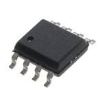
ICGOO电子元器件商城为您提供THS3121CD由Texas Instruments设计生产,在icgoo商城现货销售,并且可以通过原厂、代理商等渠道进行代购。 THS3121CD价格参考¥25.09-¥46.62。Texas InstrumentsTHS3121CD封装/规格:线性 - 放大器 - 仪表,运算放大器,缓冲器放大器, 电流反馈 放大器 1 电路 8-SOIC。您可以下载THS3121CD参考资料、Datasheet数据手册功能说明书,资料中有THS3121CD 详细功能的应用电路图电压和使用方法及教程。
| 参数 | 数值 |
| -3db带宽 | 130MHz |
| 产品目录 | 集成电路 (IC)半导体 |
| 描述 | IC OPAMP CFA 130MHZ 8SOIC高速运算放大器 Sngl Lo-Noise Hi-Out Current-Feedback |
| DevelopmentKit | THS3121EVM |
| 产品分类 | Linear - Amplifiers - Instrumentation, OP Amps, Buffer Amps集成电路 - IC |
| 品牌 | Texas Instruments |
| 产品手册 | |
| 产品图片 |
|
| rohs | 符合RoHS无铅 / 符合限制有害物质指令(RoHS)规范要求 |
| 产品系列 | 放大器 IC,高速运算放大器,Texas Instruments THS3121CD- |
| 数据手册 | |
| 产品型号 | THS3121CD |
| 产品种类 | |
| 供应商器件封装 | 8-SOIC |
| 共模抑制比—最小值 | 62 dB |
| 其它名称 | 296-34200-5 |
| 包装 | 管件 |
| 单位重量 | 76 mg |
| 压摆率 | 1700 V/µs |
| 商标 | Texas Instruments |
| 增益带宽积 | - |
| 安装类型 | 表面贴装 |
| 安装风格 | SMD/SMT |
| 封装 | Tube |
| 封装/外壳 | 8-SOIC(0.154",3.90mm 宽) |
| 封装/箱体 | SOIC-8 |
| 工作温度 | 0°C ~ 70°C |
| 工作电源电压 | 32 V |
| 工厂包装数量 | 75 |
| 放大器类型 | 电流反馈 |
| 最大功率耗散 | 1050 mW |
| 最大工作温度 | + 70 C |
| 最小工作温度 | 0 C |
| 标准包装 | 75 |
| 电压-电源,单/双 (±) | 10 V ~ 30 V, ±5 V ~ 15 V |
| 电压-输入失调 | 2mV |
| 电流-电源 | 7mA |
| 电流-输入偏置 | 3µA |
| 电流-输出/通道 | 490mA |
| 电源电压-最大 | 30 V |
| 电源电压-最小 | 10 V |
| 电源电流 | 8.5 mA |
| 电路数 | 1 |
| 系列 | THS3121 |
| 设计资源 | http://www.digikey.com/product-highlights/cn/zh/texas-instruments-webench-design-center/3176 |
| 转换速度 | 900 V/us |
| 输入补偿电压 | 6 mV |
| 输出类型 | - |
| 通道数量 | 1 Channel |
| 配用 | /product-detail/zh/THS3110EVM/296-18841-ND/863674/product-detail/zh/THS3111EVM/296-18842-ND/863675/product-detail/zh/THS3120EVM/296-18843-ND/863676 |


- 商务部:美国ITC正式对集成电路等产品启动337调查
- 曝三星4nm工艺存在良率问题 高通将骁龙8 Gen1或转产台积电
- 太阳诱电将投资9.5亿元在常州建新厂生产MLCC 预计2023年完工
- 英特尔发布欧洲新工厂建设计划 深化IDM 2.0 战略
- 台积电先进制程称霸业界 有大客户加持明年业绩稳了
- 达到5530亿美元!SIA预计今年全球半导体销售额将创下新高
- 英特尔拟将自动驾驶子公司Mobileye上市 估值或超500亿美元
- 三星加码芯片和SET,合并消费电子和移动部门,撤换高东真等 CEO
- 三星电子宣布重大人事变动 还合并消费电子和移动部门
- 海关总署:前11个月进口集成电路产品价值2.52万亿元 增长14.8%


PDF Datasheet 数据手册内容提取
THS3120 THS3121 www.ti.com........................................................................................................................................ SLOS420E–SEPTEMBER2003–REVISEDOCTOBER2009 LOW-NOISE, HIGH-OUTPUT DRIVE, CURRENT-FEEDBACK OPERATIONAL AMPLIFIERS CheckforSamples:THS3120THS3121 FEATURES DESCRIPTION 1 • LowNoise: The THS3120 and THS3121 are low-noise, 23 – 1pA/√HzNoninvertingCurrentNoise high-voltage, high output current drive, current-feedback amplifiers designed to operate over – 10pA/√HzInvertingCurrentNoise a wide supply range of ±5 V to ±15 V for today's – 2.5nV/√HzVoltageNoise high-performanceapplications. • HighOutputCurrentDrive:475mA The THS3120 offers a power saving mode by • HighSlewRate: providing a power-down pin for reducing the 7-mA – 1700V/μs(R =50 Ω,V =8V ) quiescent current of the device, when the device is L O PP notactive. • WideBandwidth:120MHz(G=2,R =50Ω) L • WideSupplyRange:±5Vto±15V These amplifiers provide well-regulated ac performance characteristics. Most notably, the 0.1-dB • Power-DownFeature:(THS3120Only) flat bandwidth is exceedingly high, reaching beyond 90 MHz. The unity-gain bandwidth of 130 MHz allows APPLICATIONS forgooddistortioncharacteristicsat10MHz.Coupled • VideoDistribution with high 1700-V/μs slew rate, the THS3120 and • PowerFETDriver THS3121 amplifiers allow for high output voltage swingsathighfrequencies. • PinDriver • CapacitiveLoadDriver The THS3120 and THS3121 are offered in an SOIC-8 (D) package and an MSOP-8 (DGN) PowerPAD™package. DIFFERENTIAL GAIN DIFFERENTIAL PHASE vs vs NUMBER OF LOADS NUMBER OF LOADS 0.07 Gain = 2, 0.14 Gain = 2, VIDEO DISTRIBUTION AMPLIFIER APPLICATION 0.06 RVSF == ±64195 WV,, 0.12 RVSF == ±64195 WV,, 649 W 649 W 40 IRE − NTSC and PAL, 40 IRE − NTSC and PAL, Differential Gain − %0000....00002345 Worst Case ±P1A0L0 IRE Ramp NTSC Differential Phase − deg000...0000.4681 Worst Case ±P1A0L0 IRE RamNpTSC VI 75 W +−1−51 5V V 7n5 77-LW55in WWTersansmission Line75 VWVOO((n1)) 0.01 0.02 0 0 0 1 2 3 4 5 6 7 8 0 1 2 3 4 5 6 7 8 75 W Number of 150 W Loads Number of 150 W Loads 1 Pleasebeawarethatanimportantnoticeconcerningavailability,standardwarranty,anduseincriticalapplicationsofTexas Instrumentssemiconductorproductsanddisclaimerstheretoappearsattheendofthisdatasheet. PowerPADisatrademarkofTexasInstruments. 2 Allothertrademarksarethepropertyoftheirrespectiveowners. 3 PRODUCTIONDATAinformationiscurrentasofpublicationdate. Copyright©2003–2009,TexasInstrumentsIncorporated Products conform to specifications per the terms of the Texas Instruments standard warranty. Production processing does not necessarilyincludetestingofallparameters.
THS3120 THS3121 SLOS420E–SEPTEMBER2003–REVISEDOCTOBER2009........................................................................................................................................ www.ti.com This integrated circuit can be damaged by ESD. Texas Instruments recommends that all integrated circuits be handled with appropriateprecautions.Failuretoobserveproperhandlingandinstallationprocedurescancausedamage. ESDdamagecanrangefromsubtleperformancedegradationtocompletedevicefailure.Precisionintegratedcircuitsmaybemore susceptibletodamagebecauseverysmallparametricchangescouldcausethedevicenottomeetitspublishedspecifications. TOPVIEW D, DGN TOPVIEW D, DGN THS3120 THS3121 REF 1 8 PD NC 1 8 NC VIN- 2 7 VS+ VIN- 2 7 VS+ VIN+ 3 6 VOUT VIN+ 3 6 VOUT VS- 4 5 NC VS- 4 5 NC NC = No Internal Connection NC= No Internal Connection NOTE: ThedevicewiththepowerdownoptiondefaultstotheONstateifnosignalisappliedtothePDpin.Additionally,the REFpinfunctionalrangeisfromV to(V –4V). S– S+ AVAILABLEOPTIONS(1) PACKAGEDDEVICE T A PLASTICSMALLOUTLINESOIC(D) PLASTICMSOP(DGN) (2)(3) SYMBOL THS3120CD THS3120CDGN 0°Cto+70°C AQA THS3120CDR THS3120CDGNR THS3120ID THS3120IDGN –40°Cto+85°C APN THS3120IDR THS3120IDGNR THS3121CD THS3121CDGN 0°Cto+70°C AQO THS3121CDR THS3121CDGNR THS3121ID THS3121IDGN –40°Cto+85°C APO THS3121IDR THS3121IDGNR (1) Forthemostcurrentpackageandorderinginformation,seethePackageOptionAddendumattheendofthisdocument,orseetheTI websiteatwww.ti.com. (2) Availableintapeandreel.TheRsuffixstandardquantityis2500(forexample,THS3120CDGNR). (3) ThePowerPADiselectricallyisolatedfromallotherpins. DISSIPATION RATING TABLE POWERRATING T =+125°C J PACKAGE θ (°C/W) θ (°C/W) T =+25°C T =+85°C JC JA A A D-8(1) 38.3 95 1.05W 421mW DGN-8(2) 4.7 58.4 1.71W 685W (1) ThesedataweretakenusingtheJEDECstandardlow-KtestPCB.FortheJEDECproposedhigh-KtestPCB,theθ is+95°C/Wwith JA powerratingatT =+25°Cof1.05W. A (2) Thesedataweretakenusing2oz.(56,7grams)traceandcopperpadthatissoldereddirectlytoa3inchx3inch(76,2mmx76,2mm) PCB.Forfurtherinformation,seetheApplicationInformationsectionofthisdatasheet. 2 SubmitDocumentationFeedback Copyright©2003–2009,TexasInstrumentsIncorporated ProductFolderLink(s):THS3120THS3121
THS3120 THS3121 www.ti.com........................................................................................................................................ SLOS420E–SEPTEMBER2003–REVISEDOCTOBER2009 RECOMMENDED OPERATING CONDITIONS PARAMETER MIN NOM MAX UNIT Dualsupply ±5 ±15 Supplyvoltage V Singlesupply 10 30 Commercial 0 +70 Operatingfree-airtemperature,T °C A Industrial –40 +85 Operatingjunctiontemperature,continuousoperating,T –40 +125 °C J Normalstoragetemperature,T –40 +85 °C STG ABSOLUTE MAXIMUM RATINGS(1) Overoperatingfree-airtemperature,unlessotherwisenoted. PARAMETER UNIT Supplyvoltage,V toV 33V S– S+ Inputvoltage,V ±V I S Differentialinputvoltage,V ±4V ID Outputcurrent,I (2) 550mA O Continuouspowerdissipation SeeDissipationRatingsTable Maximumjunctiontemperature,T (3) +150°C J Maximumjunctiontemperature,continuousoperation,long-termreliability,T (4) +125°C J Commercial 0°Cto+70°C Operatingfree-airtemperature,T A Industrial –40°Cto+85°C Storagetemperature,T –65°Cto+125°C STG HBM 1000 ESDratings: CDM 1500 MM 200 (1) Stressesbeyondthoselistedunderabsolutemaximumratingsmaycausepermanentdamagetothedevice.Thesearestressratings only,andfunctionaloperationofthedeviceattheseoranyotherconditionsbeyondthoseindicatedunderrecommendedoperating conditionsisnotimplied.Exposuretoabsolute-maximum-ratedconditionsforextendedperiodsmayaffectdevicereliability. (2) TheTHS3120andTHS3121mayincorporateaPowerPADontheundersideofthechip.Thisactsasaheatsinkandmustbeconnected toathermallydissipatingplaneforproperpowerdissipation.Failuretodosomayresultinexceedingthemaximumjunctiontemperature whichcouldpermanentlydamagethedevice.SeeTITechnicalBriefSLMA002formoreinformationaboutusingthePowerPAD thermally-enhancedpackage. (3) Theabsolutemaximumtemperatureunderanyconditionislimitedbytheconstraintsofthesiliconprocess. (4) Themaximumjunctiontemperatureforcontinuousoperationislimitedbythepackageconstraints.Operationabovethistemperature mayresultinreducedreliabilityand/orlifetimeofthedevice. Copyright©2003–2009,TexasInstrumentsIncorporated SubmitDocumentationFeedback 3 ProductFolderLink(s):THS3120THS3121
THS3120 THS3121 SLOS420E–SEPTEMBER2003–REVISEDOCTOBER2009........................................................................................................................................ www.ti.com ELECTRICAL CHARACTERISTICS AtV =±15V,R =649Ω,R =50Ω,andG=2,unlessotherwisenoted. S F L TYP OVERTEMPERATURE 0°Cto –40°Cto MIN/TYP/ PARAMETER TESTCONDITIONS +25°C +25°C +70°C +85°C UNIT MAX ACPERFORMANCE G=1,RF=806Ω,VO=200mVPP 130 G=2,RF=649Ω,VO=200mVPP 120 Small-signalbandwidth,–3dB G=5,RF=499Ω,VO=200mVPP 105 MHz TYP G=10,RF=301Ω,VO=200mVPP 66 0.1-dBbandwidthflatness G=2,RF=649Ω,VO=200mVPP 90 Large-signalbandwidth G=5,RF=499Ω,VO=2VPP 80 G=1,VO=4-Vstep,RF=806Ω 1500 Slewrate(25%to75%level) V/µs TYP G=2,VO=8-Vstep,RF=649Ω 1700 RecommendedmaximumSRfor Slewrate repetitivesignals(1) 900 V/µs MAX Riseandfalltime G=–5,VO=10-Vstep,RF=499Ω 10 ns TYP Settlingtimeto0.1% G=–2,VO=2VPPstep 11 ns TYP Settlingtimeto0.01% G=–2,VO=2VPPstep 52 Harmonicdistortion RL=50Ω 51 2ndharmonicdistortion G=2, RF=649Ω, RL=499Ω 53 dBc TYP 3rdharmonicdistortion Vf=O1=02MVHPPz, RL=50Ω 50 RL=499Ω 65 Inputvoltagenoise f>20kHz 2.5 nV/√Hz TYP Noninvertinginputcurrentnoise f>20kHz 1 pA/√Hz TYP Invertinginputcurrentnoise f>20kHz 10 pA/√Hz TYP NTSC 0.007% Differentialgain G=2, PAL 0.007% RL=150Ω, TYP Differentialphase RF=649Ω NTSC 0.018° PAL 0.022° DCPERFORMANCE Transimpedance VO=±3.75V,Gain=1 1.9 1.3 1 1 MΩ MIN Inputoffsetvoltage 3 10 12 13 mV MAX VCM=0V Averageoffsetvoltagedrift ±10 ±10 μV/°C TYP Noninvertinginputbiascurrent 1 4 6 6 μA MAX VCM=0V Averagebiascurrentdrift ±10 ±10 nA/°C TYP Invertinginputbiascurrent 3 15 20 20 μA MAX VCM=0V Averagebiascurrentdrift ±10 ±10 nA/°C TYP Inputoffsetcurrent 4 15 20 20 μA MAX VCM=0V Averageoffsetcurrentdrift ±30 ±30 nA/°C TYP INPUTCHARACTERISTICS Inputcommon-modevoltagerange ±12.7 ±12.5 ±12.2 ±12.2 V MIN Common-moderejectionratio VCM=±12.5V 70 63 60 60 dB MIN Noninvertinginputresistance 41 MΩ TYP Noninvertinginputcapacitance 0.4 pF TYP OUTPUTCHARACTERISTICS RL=1kΩ ±14 ±13.5 ±13 ±13 Outputvoltageswing V MIN RL=50Ω ±13.5 ±12.5 ±12 ±12 Outputcurrent(sourcing) RL=25Ω 475 425 400 400 mA MIN Outputcurrent(sinking) RL=25Ω 490 425 400 400 mA MIN Outputimpedance f=1MHz,closedloop 0.04 Ω TYP (1) Formoreinformation,seetheApplicationInformationsectionofthisdatasheet. 4 SubmitDocumentationFeedback Copyright©2003–2009,TexasInstrumentsIncorporated ProductFolderLink(s):THS3120THS3121
THS3120 THS3121 www.ti.com........................................................................................................................................ SLOS420E–SEPTEMBER2003–REVISEDOCTOBER2009 ELECTRICAL CHARACTERISTICS (continued) AtV =±15V,R =649Ω,R =50Ω,andG=2,unlessotherwisenoted. S F L TYP OVERTEMPERATURE 0°Cto –40°Cto MIN/TYP/ PARAMETER TESTCONDITIONS +25°C +25°C +70°C +85°C UNIT MAX POWERSUPPLY Specifiedoperatingvoltage ±15 ±16 ±16 ±16 V MAX Maximumquiescentcurrent 7 8.5 11 11 mA MAX Minimumquiescentcurrent 7 5.5 4 4 mA MIN Power-supplyrejection(+PSRR) VS+=15.5Vto14.5V,VS–=15V 75 65 60 60 dB MIN Power-supplyrejection(–PSRR) VS+=15V,VS–=–15.5Vto–14.5V 69 60 55 55 dB MIN POWER-DOWNCHARACTERISTICS(THS3120Only) REFvoltagerange(2) VS+–4 V MAX VS– MIN PD≤REF Enable MIN +0.8 Power-downvoltagelevel(2) V PD≥REF Disable MAX +2 Power-downquiescentcurrent PD≥REF+2V 300 450 500 500 μA MAX VPD=0V,REF=0V, 11 PDpinbiascurrent μA TYP VPD=3.3V,REF=0V 11 Turn-ontimedelay 90%offinalvalue 4 μs TYP Turn-offtimedelay 10%offinalvalue 6 Inputimpedance 3.4||1.7 kΩ||pF TYP (2) Formoreinformation,seetheApplicationInformationsectionofthisdatasheet. Copyright©2003–2009,TexasInstrumentsIncorporated SubmitDocumentationFeedback 5 ProductFolderLink(s):THS3120THS3121
THS3120 THS3121 SLOS420E–SEPTEMBER2003–REVISEDOCTOBER2009........................................................................................................................................ www.ti.com ELECTRICAL CHARACTERISTICS AtV =±5V,R =750Ω,R =50Ω,andG=2,unlessotherwisenoted. S F L TYP OVERTEMPERATURE 0°Cto –40°Cto MIN/TYP/ PARAMETER TESTCONDITIONS +25°C +25°C +70°C +85°C UNIT MAX ACPERFORMANCE G=1,RF=909Ω,VO=200mVPP 105 G=2,RF=750Ω,VO=200mVPP 100 Small-signalbandwidth,–3dB G=5,RF=499Ω,VO=200mVPP 95 MHz TYP G=10,RF=301Ω,VO=200mVPP 70 0.1-dBbandwidthflatness G=2,RF=750Ω,VO=200mVPP 70 Large-signalbandwidth G=2,RF=750Ω,VO=2VPP 85 G=1,VO=2-Vstep,RF=909Ω 560 Slewrate(25%to75%level) V/μs TYP G=2,VO=2-Vstep,RF=750Ω 620 RecommendedmaximumSRfor Slewrate repetitivesignals(1) 900 V/μs MAX Riseandfalltime G=–5,VO=5-Vstep,RF=499Ω 10 ns TYP Settlingtimeto0.1% G=–2,VO=2VPPstep 7 ns TYP Settlingtimeto0.01% G=–2,VO=2VPPstep 42 Harmonicdistortion RL=50Ω 51 2ndharmonicdistortion G=2, RF=649Ω, RL=499Ω 53 dBc TYP 3rdharmonicdistortion Vf=O1=02MVHPPz, RL=50Ω 48 RL=499Ω 60 Inputvoltagenoise f>20kHz 2.5 nV/√Hz TYP Noninvertinginputcurrentnoise f>20kHz 1 pA/√Hz TYP Invertinginputcurrentnoise f>20kHz 10 pA/√Hz TYP NTSC 0.008% Differentialgain G=2, PAL 0.008% RL=150Ω, TYP Differentialphase RF=806Ω NTSC 0.014° PAL 0.018° DCPERFORMANCE Transimpedance VO=±1.25V,gain=1 1.2 0.9 0.7 0.7 MΩ MIN Inputoffsetvoltage 6 10 12 13 mV MAX VCM=0V Averageoffsetvoltagedrift ±10 ±10 µV/°C TYP Noninvertinginputbiascurrent 1 4 6 6 μA MAX VCM=0V Averagebiascurrentdrift ±10 ±10 nA/°C TYP Invertinginputbiascurrent 2 15 20 20 μA MAX VCM=0V Averagebiascurrentdrift ±10 ±10 nA/°C TYP Inputoffsetcurrent 2 15 20 20 μA MAX VCM=0V Averageoffsetcurrentdrift ±30 ±30 nA/°C TYP INPUTCHARACTERISTICS Inputcommon-modevoltagerange ±2.7 ±2.5 ±2.3 ±2.3 V MIN Common-moderejectionratio VCM=±2.5V 66 62 58 58 dB MIN Noninvertinginputresistance 35 MΩ TYP Noninvertinginputcapacitance 0.5 pF TYP OUTPUTCHARACTERISTICS RL=1kΩ ±4 ±3.8 ±3.7 ±3.7 Outputvoltageswing V MIN RL=50Ω ±3.9 ±3.7 ±3.6 ±3.6 Outputcurrent(sourcing) RL=10Ω 310 250 200 200 mA MIN Outputcurrent(sinking) RL=10Ω 325 250 200 200 mA MIN Outputimpedance f=1MHz 0.05 Ω TYP (1) Formoreinformation,seetheApplicationInformationsectionofthisdatasheet. 6 SubmitDocumentationFeedback Copyright©2003–2009,TexasInstrumentsIncorporated ProductFolderLink(s):THS3120THS3121
THS3120 THS3121 www.ti.com........................................................................................................................................ SLOS420E–SEPTEMBER2003–REVISEDOCTOBER2009 ELECTRICAL CHARACTERISTICS (continued) AtV =±5V,R =750Ω,R =50Ω,andG=2,unlessotherwisenoted. S F L TYP OVERTEMPERATURE 0°Cto –40°Cto MIN/TYP/ PARAMETER TESTCONDITIONS +25°C +25°C +70°C +85°C UNIT MAX POWERSUPPLY Specifiedoperatingvoltage ±5 ±4.5 ±4.5 ±4.5 V MIN Maximumquiescentcurrent 6.5 8 10 10 mA MAX Minimumquiescentcurrent 6.5 4 3.5 3.5 mA MIN Power-supplyrejection(+PSRR) VS+=5.5Vto4.5V, 71 62 57 57 dB MIN VS–=5V Power-supplyrejection(–PSRR) VS+=5V, 66 57 52 52 dB MIN VS-=–5.5Vto–4.5V POWER-DOWNCHARACTERISTICS(THS3120Only) REFvoltagerange(2) VS+–4 V MAX VS– MIN PD≤REF Enable MIN +0.8 Power-downvoltagelevel(2) V PD≥REF Disable MAX +2 Power-downquiescentcurrent PD≥REF+2V 200 450 500 500 µA MAX VPD=0V,REF=0V, 11 PDpinbiascurrent μA TYP VPD=3.3V,REF=0V 11 Turn-ontimedelay 90%offinalvalue 4 μs TYP Turn-offtimedelay 10%offinalvalue 6 Inputimpedance 3.4||1.7 kΩ||pF TYP (2) Formoreinformation,seetheApplicationInformationsectionofthisdatasheet. Copyright©2003–2009,TexasInstrumentsIncorporated SubmitDocumentationFeedback 7 ProductFolderLink(s):THS3120THS3121
THS3120 THS3121 SLOS420E–SEPTEMBER2003–REVISEDOCTOBER2009........................................................................................................................................ www.ti.com TYPICAL CHARACTERISTICS TABLE OF GRAPHS ±15-VGraphs FIGURE Noninvertingsmall-signalgainfrequencyresponse 1,2 Invertingsmall-signalgainfrequencyresponse 3 0.1-dBflatness 4 Noninvertinglarge-signalgainfrequencyresponse 5 Invertinglarge-signalgainfrequencyresponse 6 Frequencyresponsecapacitiveload 7 RecommendedR vsCapacitiveload 8 ISO 2ndharmonicdistortion vsFrequency 9 3rdharmonicdistortion vsFrequency 10 Harmonicdistortion vsOutputvoltageswing 11,12 Slewrate vsOutputvoltagestep 13,14 Noise vsFrequency 15 Settlingtime 16,17 Quiescentcurrent vsSupplyvoltage 18 Outputvoltage vsLoadresistance 19 Inputbiasandoffsetcurrent vsCasetemperature 20 Inputoffsetvoltage vsCasetemperature 21 Transimpedance vsFrequency 22 Rejectionratio vsFrequency 23 Noninvertingsmall-signaltransientresponse 24 Invertinglarge-signaltransientresponse 25 Overdriverecoverytime 26 Differentialgain vsNumberofloads 27 Differentialphase vsNumberofloads 28 Closed-loopoutputimpedance vsFrequency 29 Power-downquiescentcurrent vsSupplyvoltage 30 Turn-onandturn-offtimedelay 31 ±5-VGraphs FIGURE Noninvertingsmall-signalgainfrequencyresponse 32 Invertingsmall-signalgainfrequencyresponse 33 0.1-dBflatness 34 Slewrate vsOutputvoltagestep 35,36 2ndharmonicdistortion vsFrequency 37 3rdharmonicdistortion vsFrequency 38 Harmonicdistortion vsOutputvoltageswing 39,40 Noninvertingsmall-signaltransientresponse 41 Invertingsmall-signaltransientresponse 42 Inputbiasandoffsetcurrent vsCasetemperature 43 Overdriverecoverytime 44 Settlingtime 45 Rejectionratio vsFrequency 46 8 SubmitDocumentationFeedback Copyright©2003–2009,TexasInstrumentsIncorporated ProductFolderLink(s):THS3120THS3121
THS3120 THS3121 www.ti.com........................................................................................................................................ SLOS420E–SEPTEMBER2003–REVISEDOCTOBER2009 TYPICAL CHARACTERISTICS (±15 V) blank NONINVERTINGSMALL-SIGNAL NONINVERTINGSMALL-SIGNAL INVERTINGSMALL-SIGNAL FREQUENCYRESPONSE FREQUENCYRESPONSE FREQUENCYRESPONSE 9 24 24 78 RFR =F 6 =4 94 7W5 W 122802 G = 10, RF = 301 W RVVOSL === 5±001.2 5W VV,PP, 122802 G = -10, RF = 365 W VOVR =SL 0 ==. 2 ±5 1V05 PW PV,, g Gain − dB 56 RF = 750 W g Gain − dB 11110246 G = 5, RF = 499 W Gain - dB 11110246 G = -5, RF = 499 W oninvertin 34 Gain = 2, oninvertin 468 G = 2, RF = 649 W Inverting 468 G = -2, RF = 681 W N 2 RL = 50 W , N 2 G = 1, RF = 806 W 2 1 VVOS == ±01.25 VVPP, −02 -20 G = -1, RF = 681 W 0 −4 -4 1 M 10 M 100 M 1 G 100 k 1 M 10 M 100 M 1 G 100 k 1 M 10 M 100 M 1 G f − Frequency − Hz f − Frequency − Hz f - Frequency - Hz Figure1. Figure2. Figure3. NONINVERTINGLARGE-SIGNAL INVERTINGLARGE-SIGNAL 0.1-dBFLATNESS FREQUENCYRESPONSE FREQUENCYRESPONSE 6.3 16 16 6.2 GRFa i=n =56 22, W , 14 G = 5, RF = 499 W 14 G = -5, RF = 499 W Noninverting Gain - dB 56..916 RVVOSL === 5±001.2 5W VV,PP, Noninverting Gain − dB 1102468 G = 2, RF = 681 W Inverting Gain - dB 11022468 G =-1, RF = 681 W 5.8 2 RVVOSL === 5±201 V 5WP V,P, -20 RVVOSL === 5±201 V 5WP V,P, 5.7 0 -4 100 k 1 M 10 M 100 M 100 k 1 M 10 M 100 M 1 G 1 M 10 M 100 M 1 G f - Frequency - Hz f − Frequency − Hz f - Frequency - Hz Figure4. Figure5. Figure6. RECOMMENDEDR 2ndHARMONICDISTORTION ISO FREQUENCYRESPONSE vs vs CAPACITIVELOAD CAPACITIVELOAD FREQUENCY 16 60 -30 R(ISO) = 49.9 W CL = 10 pF Gain = 5, VO = 2 VPP, Signal Gain - dB 11102402468 GRLa i=n 5=0 5 WR,(RIRSC(O(CIISCLS)L OOL== ) =) = 14= = 200 4 220.3720 0 p p p WWFFWF WRecommended RResistance −ISO 1234500000 RVSL == 5±01 5W V, 2 nd Harmonic Distortion - dBc ------987654000000 RVGRSL F === = 5±5 014, 59W 9V, W GRL = = 2 4, 9R9F W= 64GR9F = W= 2, 6, 49 W -2 VS = ±15 V 0 -100 10 M 100 M 10 100 100 k 1 M 10 M 100 M Capacitive Load - Hz CL − Capacitive Load − pF f - Frequency - Hz Figure7. Figure8. Figure9. Copyright©2003–2009,TexasInstrumentsIncorporated SubmitDocumentationFeedback 9 ProductFolderLink(s):THS3120THS3121
THS3120 THS3121 SLOS420E–SEPTEMBER2003–REVISEDOCTOBER2009........................................................................................................................................ www.ti.com TYPICAL CHARACTERISTICS (±15 V) (continued) blank 3rdHARMONICDISTORTION HARMONICDISTORTION HARMONICDISTORTION vs vs vs FREQUENCY OUTPUTVOLTAGESWING OUTPUTVOLTAGESWING -30 -70 -40 VO = 2 VPP, HD2, RL = 50W 3rd Harmonic Distortion - dBc -1------09876540000000 RVGRSLF = === 2 5±6, 014 59GRW FV ,W= = 5 4,99 W GRRFL = == 2 46, 9499 WW , Harmonic Distortion - dBc-1-----099887050505 HD2, RL = 499W HHDD33, ,GRfV R=RSFa L1L i ==n = = M±6= 4541 9H20959,zW WWV, Harmonic Distortion - dBc -----9876500000 HHDD32,, RRHLLD =2= , 4 5R90L9 W W= 4H9D93W, RGRfV L=SFa = i8==n 5 ±6=M041 2HW95, zWV, 100 k 1 M 10 M 100 M 0 1 2 3 4 5 6 7 8 9 10 0 1 2 3 4 5 6 7 8 9 10 f - Frequency - Hz VO - Output Voltage Swing - VPP VO - Output Voltage Swing - VPP Figure10. Figure11. Figure12. SLEWRATE SLEWRATE NOISE vs vs vs OUTPUTVOLTAGESTEP OUTPUTVOLTAGESTEP FREQUENCY 2000 2000 100 Gain = 1 Gain = 2 11680000 RRLF == 5800 6W W 11680000 RRLF == 5604 9W W Hz Hz msSR − Slew Rate − V/ 111024680000000000 VS = ±15 V Rise Fall msSR − Slew Rate − V/ 111024680000000000 VS = ±15 V Rise Fall - Voltage Noise - nV/n- Current Noise -pA/n10 In-Vn 400 400 V I 200 200 In+ 0 0 1 0 0.5 1 1.5 2 2.5 3 3.5 4 4.5 5 0 1 2 3 4 5 6 7 8 9 10 0.01 0.1 1 10 100 VO − Output Voltage −VPP VO − Output Voltage −VPP f - Frequency - kHz Figure13. Figure14. Figure15. QUIESCENTCURRENT vs SETTLINGTIME SETTLINGTIME SUPPLYVOLTAGE 1.25 4.5 10 1 Rising Edge 3.54 9 TA = 85 °C 0.75 2.53 Rising Edge mA 8 TA = 25 °C − Output Voltage − VVO−−−000.0..0272..550555 FallinGRRVgSLFa iE===n d5=±4g091 e− 95W2 WV − Output Voltage − VVO−−−01210−−−.....55012555321 GRRVSLFa i===n 5=±4091 − 95W2 WV - Quiescent Current - IQ 234567 TA = -40 °C Falling Edge −1 −3.5 1 −4 −1.25 −4.5 0 0 2 4 6 8 10 12 14 16 0 2 4 6 8 10 12 14 16 2 3 4 5 6 7 8 9 101112131415 t − Time − ns t − Time − ns VS - Supply Voltage - ±V Figure16. Figure17. Figure18. 10 SubmitDocumentationFeedback Copyright©2003–2009,TexasInstrumentsIncorporated ProductFolderLink(s):THS3120THS3121
THS3120 THS3121 www.ti.com........................................................................................................................................ SLOS420E–SEPTEMBER2003–REVISEDOCTOBER2009 TYPICAL CHARACTERISTICS (±15 V) (continued) blank INPUTBIASAND OUTPUTVOLTAGE OFFSETCURRENT INPUTOFFSETVOLTAGE vs vs vs LOADRESISTANCE CASETEMPERATURE CASETEMPERATURE 16 4 6 14 VS = ±15 V − Output Voltage − VVO −−−−−−11110202468208642 VTAS == −±4105 tVo 85°C m− Input Bias Current −AIIBm− Input Offset Current −AIOS0123....5555123 IIB− IIB+IOS − Input Offset Voltage − mVVOS 12345 VS = ±15 V VS = ±5 V −14 −16 0 0 10 100 1000 −40−30−20−100 102030405060708090 −40−30−20−10 0 10203040506070 8090 RL − Load Resistance − W TC − Case Temperature − °C TC − Case Temperature − °C Figure19. Figure20. Figure21. TRANSIMPEDANCE REJECTIONRATIO vs vs NONINVERTINGSMALL-SIGNAL FREQUENCY FREQUENCY TRANSIENTRESPONSE 100 70 0.3 90 CMRR VS = ±15 V 0.25 s 60 0.2 Output m 80 Transimpedance Gain - dB oh 12345670000000 VS = ±5 V VS = ±15 V Rejection Ratio − dB 1234500000 PSRR+ PSRR− - Output Voltage - VVO---000--000...0..0210.01.1.55525510 GRRVSLFa iI===nn p5±6=u041 2t 95W, WV,, 0 0 -0.3 100 k 1 M 10 M 100 M 1 G 100 k 1 M 10 M 100 M 0.04 0.05 0.06 0.07 0.08 0.09 0.1 0.11 0.12 f - Frequency - Hz f − Frequency − Hz t - Time - m s Figure22. Figure23. Figure24. Copyright©2003–2009,TexasInstrumentsIncorporated SubmitDocumentationFeedback 11 ProductFolderLink(s):THS3120THS3121
THS3120 THS3121 SLOS420E–SEPTEMBER2003–REVISEDOCTOBER2009........................................................................................................................................ www.ti.com TYPICAL CHARACTERISTICS (±15 V) (continued) blank DIFFERENTIALGAIN INVERTINGLARGE-SIGNAL vs TRANSIENTRESPONSE OVERDRIVERECOVERYTIME NUMBEROFLOADS 6 20 4 0.07 Gain = 2, Gain = 2, - Output Voltage - VVO ---321012345 GaiInn p=Ou u-t5tp,ut Output Voltage - V-1-11050505 RVSF == ±64185 WV, --012321 - Input Voltage - VVI Differential Gain − % 00000.....0000023456 RV4W0SFo Ir==Rs tE±6 C41 −95a sNWVeT,, S±P1AC0L a0n IdR EP ARLa,mp NTSC -4 RRLF == 5409 9W W,, -15 -3 0.01 -5 VS = ±15 V -20 -4 -6 0 0.2 0.4 0.6 0.8 1 0 0.04 0.05 0.06 0.07 0.08 0.09 0.1 0.11 0.12 0 1 2 3 4 5 6 7 8 t - Time - m s t - Time - m s Number of 150 W Loads Figure25. Figure26. Figure27. CLOSED-LOOPOUTPUT POWER-DOWNQUIESCENT DIFFERENTIALPHASE IMPEDANCE CURRENT vs vs vs NUMBEROFLOADS FREQUENCY SUPPLYVOLTAGE 0.14 100 400 °Differential Phase - 00000.....000001.246821 GRV4W0SFao iIr==nRs tE±6= C41 2-95a ,N sWVTe,, S±PC1A0 aL0n IdR PEA RL,amNpTSC W− Closed-Loop Output Impedance − 01.101 GRVSFa i==n ±6=41 295, WV, mAPowerdown Quiescent Current − 11223305050550000000 TA = T8A5 °=C 25°C TA = −40°C O 0 Z 0.01 0 0 1 2 3 4 5 6 7 8 1 M 10 M 100 M 1 G 3 5 7 9 11 13 15 Number of 150 W Loads f − Frequency − Hz VS − Supply Voltage − ±V Figure28. Figure29. Figure30. TURN-ONANDTURN-OFF TIMEDELAY 1.5 1 V − 0.5 Output Voltage el V Lev 0 e − ge −0.5 Powerdown Pulse 6 uls Volta 5 wn P ut 4 Do utp 3 wer O o − O Gain = 5, 2 P V VI = 0.1 Vdc 1 RVSL == 5±01 5W V and ±5 V 0 −1 0 0.1 0.2 0.3 0.4 0.5 0.6 0.7 t − Time − ms Figure31. 12 SubmitDocumentationFeedback Copyright©2003–2009,TexasInstrumentsIncorporated ProductFolderLink(s):THS3120THS3121
THS3120 THS3121 www.ti.com........................................................................................................................................ SLOS420E–SEPTEMBER2003–REVISEDOCTOBER2009 TYPICAL CHARACTERISTICS (±5 V) blank NONINVERTINGSMALL-SIGNAL INVERTINGSMALL-SIGNAL FREQUENCYRESPONSE FREQUENCYRESPONSE 0.1-dBFLATNESS 24 24 6.3 oninverting Gain − dB 11111220246802468 GG G= =1= 0 52,, , R RRFFF = == 3 47095190 W WW RVVOSL === 5±005.2 WV V,PP, Inverting Gain - dB 11111220246802468 GG = =-G1 -05 =,, RR-2FF, ==R F34 69=59 6 WW81 W RVVOSL === 5±005.2 WV V,PP, Noninverting Gain - dB 566...9126 GRRVVOSFLa i===n= 5±=70055 .22 0WV, VW,P,P, N 2 G = 1, RF = 909 W 2 G = -1, RF = 750 W 5.8 0 0 −2 -2 −4 -4 5.7 1 M 10 M 100 M 1 G 1 M 10 M 100 M 1 G 1 M 10 M 100 M f − Frequency − Hz f - Frequency - Hz f - Frequency - Hz Figure32. Figure33. Figure34. SLEWRATE SLEWRATE 2ndHARMONICDISTORTION vs vs vs OUTPUTVOLTAGESTEP OUTPUTVOLTAGESTEP FREQUENCY 700 700 -30 Gain = 1 Rise Rise s 600 RRVSLF === 5±9005 9 WV W s 600 dBc -40 G = -5, RF = 499 W mSR − Slew Rate − V/ 234500000000 Fall mSR − Slew Rate − V/ 234500000000 Fall armonic Destortion - ----87650000 G = -2, RF = 649 W Gain = 2 H 100 100 RRVSLF === 5±7055 0 WV W 2nd -90 VRVOSL === 1±205 V0 VP WP,, 0 0 -100 0 1 2 3 4 5 0 1 2 3 4 5 6 7 100 k 1 M 10 M 100 M VO − Output Voltage −VPP VO − Output Voltage −VPP f - Frequency - Hz Figure35. Figure36. Figure37. 3rdHARMONICDISTORTION HARMONICDISTORTION HARMONICDISTORTION vs vs vs FREQUENCY OUTPUTVOLTAGESWING OUTPUTVOLTAGESWING -30 -70 -40 dBc -40 VRVOSL === 1±205 V0 VP WP,, Bc -75 HD3, RL = 50W HD3, RL = 50W Bc -50 HD3, RL = 50W HD3, RL = 50W 3rd Harmonic Distortion - -----9876500000 G = -5, RGF == -429, 9R WF = 649 W Harmonic Distortion - d ----99885050 GRfV=SFa 1 i==n M ±6=H45 29 zV,H WD3, RHLD =2 ,4 R99L W= 499W Harmonic Distortion - d ---876000 HD3, RLH =D 24,9 R9WL = 499GRfVW=SFa 8 i==n M ±6=H45 29 zV, W -100 -100 -90 100 k 1 M 10 M 100 M 0 0.5 1 1.5 2 2.5 3 3.5 4 4.5 5 0 0.5 1 1.5 2 2.5 3 3.5 4 4.5 5 f - Frequency - Hz VO - Output Voltage Swing - VPP VO - Output Voltage Swing - VPP Figure38. Figure39. Figure40. Copyright©2003–2009,TexasInstrumentsIncorporated SubmitDocumentationFeedback 13 ProductFolderLink(s):THS3120THS3121
THS3120 THS3121 SLOS420E–SEPTEMBER2003–REVISEDOCTOBER2009........................................................................................................................................ www.ti.com TYPICAL CHARACTERISTICS (±5 V) (continued) blank INPUTBIASAND OFFSETCURRENT NONINVERTINGSMALL-SIGNAL INVERTINGLARGE-SIGNAL vs TRANSIENTRESPONSE TRANSIENTRESPONSE CASETEMPERATURE 0.3 3.5 2 0.25 3 VS = ±5 V 0.2 Output 2.5 Output A A 1.75 - Output Voltage - VVO---000--00...00..021001...555215510 GRRVSLFa iI===nn p75±=u505 2t0 WV W - Output Voltage - VVO ---21001---.....55532155012 GRRVSLFaI n i===np u5±=4t095 - 9 5WV ,W,, m− Input Bias Current −IIBm− Input Offset Current −IOS001...01272..555551 IIB− IOSIIB+ -0.3 -3.5 0 0 10 20 30 40 50 60 70 0 10 20 30 40 50 60 70 −40−30−20−100 102030405060708090 t - Time - ns t - Time - m s TC − Case Temperature − °C Figure41. Figure42. Figure43. REJECTIONRATIO vs OVERDRIVERECOVERYTIME SETTLINGTIME FREQUENCY 5 1 1.25 70 4 Gain = 2, 0.8 1 VS = ±5 V - Output Voltage - VVO ---3210123 RVSF == ±7550 V W , ---0000000...246...642- Input Voltage - VVI − Output Voltage − VVO−−000..0.0272..555055 GRRVSLFa i===nR 5=±6is085 −i 1 nWV2 gW Edge Rejection Ratio − dB 2345600000 CMRR PSRR− −0.75 -4 -0.8 Falling Edge 10 PSRR+ −1 -5 -1 0 0.2 0.4 0.6 0.8 1 −1.25 0 t - Time - m s 0 2 4 6 8 101214161820222426 100 k 1 M 10 M 100 M t − Time − ns f − Frequency − Hz Figure44. Figure45. Figure46. 14 SubmitDocumentationFeedback Copyright©2003–2009,TexasInstrumentsIncorporated ProductFolderLink(s):THS3120THS3121
THS3120 THS3121 www.ti.com........................................................................................................................................ SLOS420E–SEPTEMBER2003–REVISEDOCTOBER2009 APPLICATION INFORMATION MAXIMUM SLEW RATE FOR REPETITIVE Current-feedback amplifiers are highly dependent on SIGNALS the feedback resistor R for maximum performance F The THS3120 and THS3121 are recommended for and stability. Table 1 shows the optimal gain setting high slew rate pulsed applications where the internal resistors RF and RG at different gains to give nodes of the amplifier have time to stabilize between maximum bandwidth with minimal peaking in the pulses. It is recommended to have at least 20-ns frequency response. Higher bandwidths can be delaybetweenpulses. achieved, at the expense of added peaking in the frequency response, by using even lower values for The THS3120 and THS3121 are not recommended R . Conversely, increasing R decreases the F F for applications with repetitive signals (sine, square, bandwidth,butstabilityisimproved. sawtooth, or other) that exceed 900 V/μs. Using the part in these applications results in excessive current Table1.RecommendedResistorValuesfor draw from the power supply and possible device OptimumFrequencyResponse damage. THS3120ANDTHS3121R ANDR VALUESFORMINIMAL F G Forapplicationswithhighslewrate,repetitivesignals, PEAKINGWITHRL=50Ω theTHS3091andTHS3095(single),orTHS3092and SUPPLYVOLTAGE THS3096(dual)arerecommended. GAIN(V/V) (V) RG(Ω) RF(Ω) ±15 — 806 1 WIDEBAND, NONINVERTING OPERATION ±5 — 909 The THS3120 and THS3121 are unity-gain stable ±15 649 649 2 130-MHz current-feedback operational amplifiers, ±5 750 750 designed to operate from a ±5-V to ±15-V power ±15 124 499 supply. 5 ±5 124 499 Figure 47 shows the THS3121 in a noninverting gain ±15 33.2 301 10 of 2-V/V configuration typically used to generate the ±5 33.2 301 Typical Characteristics. Most of the curves were ±15 681 681 characterized using signal sources with 50-Ω source –1 ±5 750 750 impedance, and with measurement equipment presentinga50-Ωloadimpedance. –2 ±15and±5 340 681 –5 ±15and±5 100 499 15 V –10 ±15and±5 36.5 365 +VS + 50 W Source 0.1 m F 6.8 m F VI + 49.9 W 49.9 W T_HS3120 50 W LOAD RF 649 W 649 W RG 0.1 m F 6.8 m F + -VS -15 V Figure47. Wideband,NoninvertingGain Configuration Copyright©2003–2009,TexasInstrumentsIncorporated SubmitDocumentationFeedback 15 ProductFolderLink(s):THS3120THS3121
THS3120 THS3121 SLOS420E–SEPTEMBER2003–REVISEDOCTOBER2009........................................................................................................................................ www.ti.com WIDEBAND, INVERTING OPERATION +VS Figure 48 shows the THS3121 in a typical inverting 50 W Source gain configuration where the input and output impedances and signal gain from Figure 47 are VI + 49.9 W retainedinaninvertingcircuitconfiguration. RT 49.9 W T_HS3120 50 W LOAD 15 V+VS +VS RF 2 + RG 649 W 0.1 m F 6.8 m F 649 W + +VS 49.9 W 2 THS3120 RF _ 50 W LOAD 681 W 50 W Source RG RF 50 W Source VS RG _ VI R539M4 W0 W 681 W 0.1 m F 6.8 m F VI59 W R3T40 W T+HS3120 49.95 W0 W LOAD + +VS +VS -15 V -VS 2 2 Figure49. DC-Coupled,Single-SupplyOperation Figure48. Wideband,InvertingGain Configuration VideoDistribution The wide bandwidth, high slew rate, and high output SINGLE-SUPPLY OPERATION drive current of the THS3120 and THS3121 matches The THS3120 and THS3121 have the capability to the demands for video distribution for delivering video operate from a single supply voltage ranging from signals down multiple cables. To ensure high signal 10 V to 30 V. When operating from a single power quality with minimal degradation of performance, a supply, biasing the input and output at mid-supply 0.1-dB gain flatness should be at least 7x the allows for the maximum output voltage swing. The passband frequency to minimize group delay circuits of Figure 49 show inverting and noninverting variations from the amplifier. A high slew rate amplifiersconfiguredforsingle-supplyoperation. minimizes distortion of the video signal, and supports component video and RGB video signals that require fast transition times and fast settling times for high signalquality. 649 W 649 W 15 V 75 W 75-W Transmission Line VO(1) - VI + -15 V 75 W n Lines 75 W 75 W VO(n) 75 W Figure50. VideoDistributionAmplifier Application 16 SubmitDocumentationFeedback Copyright©2003–2009,TexasInstrumentsIncorporated ProductFolderLink(s):THS3120THS3121
THS3120 THS3121 www.ti.com........................................................................................................................................ SLOS420E–SEPTEMBER2003–REVISEDOCTOBER2009 DrivingCapacitiveLoads Placing a small series resistor, R , between the ISO amplifier output and the capacitive load, as shown in Applications such as FET drivers and line drivers can Figure 52, is an easy way of isolating the load be highly capacitive and cause stability problems for capacitance. high-speedamplifiers. Using a ferrite chip in place of R , as shown in Figure 51 through Figure 57 show recommended ISO Figure 53, is another approach of isolating the output methods for driving capacitive loads. The basic idea of the amplifier. The ferrite impedance characteristic is to use a resistor or ferrite chip to isolate the phase versus frequency is useful to maintain the low shift at high frequency caused by the capacitive load frequency load independence of the amplifier while from the amplifier feedback path. See Figure 51 for isolating the phase shift caused by the capacitance at recommendedresistorvaluesversuscapacitiveload. high frequency. Use a ferrite chip with similar impedance to R , 20 Ω to 50 Ω, at 100 MHz and ISO 60 lowimpedanceatdc. Gain = 5, Wnce − 50 RVSL == 5±01 5W V, Figure 54 shows another method used to maintain a the low frequency load independence of the amplifier st si 40 while isolating the phase shift caused by the e R O capacitance at high frequency. At low frequency, RIS 30 feedback is mainly from the load side of R . At high d ISO de frequency, the feedback is mainly via the 27-pF n 20 mme capacitor. The resistor RIN in series with the negative o input is used to stabilize the amplifier and should be c 10 Re equal to the recommended value of R at unity gain. F 0 Replacing RIN with a ferrite chip of similar impedance 10 100 at about 100 MHz as illustrated in Figure 55 gives CL − Capacitive Load − pF similar results with reduced dc offset and low frequency noise. (See the Additional Reference Figure51. RecommendedRISOvsCapacitive Material section for expanding the usability of Load current-feedbackamplifiers.) 499 W RF 499 W 27 pF VS 124 W _ 5.11 W 100 W LOAD RIN VS + RISO RG 750 W _ 5.11 W 100 W LOAD -VS 1 m F 124 W + VS 49.9 W -VS 1 m F 49.9 W VS Figure52. ResistortoIsolateCapacitiveLoad Figure54. FeedbackTechniquewithInput ResistorforCapacitiveLoad 499 W VS 124 W _ Ferrite Bead + 100 W LOAD -VS 1 m F 49.9 W VS Figure53. FerriteBeadtoIsolateCapacitiveLoad Copyright©2003–2009,TexasInstrumentsIncorporated SubmitDocumentationFeedback 17 ProductFolderLink(s):THS3120THS3121
THS3120 THS3121 SLOS420E–SEPTEMBER2003–REVISEDOCTOBER2009........................................................................................................................................ www.ti.com Figure 57 shows a push-pull FET driver circuit typical RF of ultrasound applications with isolation resistors to 499 W isolatethegatecapacitancefromtheamplifier. 27 pF FIN VS VS VS RG FB _ 5.11 W 100 W LOAD + 5.11 W 124 W _ + -VS 1 m F -VS 49.9 W VS 301 W 66.5 W 301 W Figure55. FeedbackTechniquewithInputFerrite BeadforCapacitiveLoad VS _ 5.11 W Figure 56 is shown using two amplifiers in parallel to + double the output drive current to larger capacitive loads. This technique is used when more output -VS -VS current is needed to charge and discharge the load Figure57. PowerFETDriveCircuit fasteraswhendrivinglargeFETtransistors. 499 W SAVING POWER WITH POWER-DOWN FUNCTIONALITY AND SETTING VS 124 W THRESHOLD LEVELS WITH THE _ 5.11 W REFERENCE PIN + 24.9 W The THS3120 features a power-down pin (PD) which -VS lowers the quiescent current from 7 mA down to 499 W 300μA,idealforreducingsystempower. VS VS 1 nF The power-down pin of the amplifier defaults to the 124 W REF pin voltage in the absence of an applied voltage, _ 5.11 W putting the amplifier in the normal on mode of + operation. To turn off the amplifier in an effort to 24.9 W conserve power, the power-down pin can be driven -VS towards the positive rail. The threshold voltages for power-on and power-down are relative to the supply Figure56. ParallelAmplifiersforHigherOutput rails and are given in the specification tables. Below Drive the Enable Threshold Voltage, the device is on. Above the Disable Threshold Voltage, the device is off. Behavior in between these threshold voltages is notspecified. Note that this power-down functionality is just that; the amplifier consumes less power in power-down mode. The power-down mode is not intended to provide a high-impedance output. In other words, the power-down functionality is not intended to allow use as a 3-state bus driver. When in power-down mode, the impedance looking back into the output of the amplifier is dominated by the feedback and gain setting resistors, but the output impedance of the device itself varies depending on the voltage applied totheoutputs. 18 SubmitDocumentationFeedback Copyright©2003–2009,TexasInstrumentsIncorporated ProductFolderLink(s):THS3120THS3121
THS3120 THS3121 www.ti.com........................................................................................................................................ SLOS420E–SEPTEMBER2003–REVISEDOCTOBER2009 Figure 58 shows the total system output impedance POWER-DOWN REFERENCE PIN which includes the amplifier output impedance in OPERATION parallel with the feedback plus gain resistors, which In addition to the power-down pin, the THS3120 cumulate to 1298 Ω. Figure 47 shows this circuit features a reference pin (REF) which allows the user configurationforreference. to control the enable or disable power-down voltage levels applied to the PD pin. In most split-supply 1400 applications, the reference pin is connected to Gain = 2 W− 1200 RF = 649 W ground. In either case, the user needs to be aware of ce VS = ±15 V and ±5 V voltage-level thresholds that apply to the power-down n da 1000 pin. Table 2 shows examples and illustrate the e mp relationship between the reference voltage and the ut I 800 power-down thresholds. In the table, the threshold p Out 600 levelsarederivedbythefollowingequations: n w PD≤ REF+0.8Vforenable do 400 er PD≥ REF+2Vfordisable w Po 200 wheretheusablerangeattheREFpinis 0 V ≤ V ≤ (V – 4V). S– REF S+ 100 k 1 M 10 M 100 M 1 G The recommended mode of operation is to tie the f − Frequency − Hz REF pin to midrail, thus settings the enable/disable threshold to V + 0.8 V and V = 2 V Figure58. Power-downOutputImpedancevs (midrail) (midrail) respectively. Frequency Table2.Power-DownThresholdVoltageLevels As with most current-feedback amplifiers, the internal REFERENCE architecture places some limitations on the system SUPPLY PIN ENABLE DISABLE when in power-down mode. Most notably is the fact VOLTAGE(V) VOLTAGE(V) LEVEL(V) LEVEL(V) thattheamplifieractuallyturnsONifthereisa±0.7V ±15,±5 0 0.8 2 or greater difference between the two input nodes ±15 2 2.8 4 (V+ and V–) of the amplifier. If this difference exceeds ±0.7 V, the output of the amplifier creates an ±15 –2 –1.2 0 output voltage equal to approximately [(V+) – (V–) – ±5 1 1.8 3 0.7 V] × Gain. Also, if a voltage is applied to the ±5 –1 –0.2 1 output while in power-down mode, the V– node 30 15 15.8 17 voltage is equal to V × R /(R + R ). For low O(applied) G F G 10 5 5.8 7 gain configurations and a large applied voltage at the output, the amplifier may actually turn ON due to the Note that if the REF pin is left unterminated, it floats aforementionedbehavior. to the positive rail and falls outside of the The time delays associated with turning the device on recommended operating range given above (VS– ≤ and off are specified as the time it takes for the VREF ≤ VS+ – 4 V). As a result, it no longer serves as amplifier to reach either 10% or 90% of the final a reliable reference for the PD pin, and the output voltage. The time delays are in the order of enable/disable thresholds given above no longer microsecondsbecausetheamplifiermovesinandout apply. If the PD pin is also left unterminated, it floats ofthelinearmodeofoperationinthesetransitions. to the positive rail and the device is disabled. If balanced, split supplies are used (±V ) and the REF S andPDpinsaregrounded,thedeviceisenabled. Copyright©2003–2009,TexasInstrumentsIncorporated SubmitDocumentationFeedback 19 ProductFolderLink(s):THS3120THS3121
THS3120 THS3121 SLOS420E–SEPTEMBER2003–REVISEDOCTOBER2009........................................................................................................................................ www.ti.com PRINTED-CIRCUIT BOARD LAYOUT • Connections to other wideband devices on the TECHNIQUES FOR OPTIMAL board may be made with short direct traces or PERFORMANCE through onboard transmission lines. For short connections, consider the trace and the input to Achieving optimum performance with high frequency the next device as a lumped capacitive load. amplifiers, like the THS3120 and THS3121, requires Relatively wide traces [0.05 inch (1,3 mm) to carefulattentiontoboardlayoutparasiticandexternal 0.1 inch (2,54 mm)] should be used, preferably component types. Recommendations that optimize with ground and power planes opened up around performanceinclude: them. Estimate the total capacitive load and • Minimize parasitic capacitance to any ac ground determine if isolation resistors on the outputs are for all of the signal I/O pins. Parasitic capacitance necessary. Low parasitic capacitive loads (less on the output and input pins can cause instability. than 4 pF) may not need an R because the S To reduce unwanted capacitance, a window THS3120 and THS3121 are nominally around the signal I/O pins should be opened in all compensated to operate with a 2-pF parasitic of the ground and power planes around those load. Higher parasitic capacitive loads without an pins. Otherwise, ground and power planes should R are allowed as the signal gain increases S beunbrokenelsewhereontheboard. (increasing the unloaded phase margin). If a long • Minimize the distance [< 0.25 inch, (6,4 mm)] from trace is required, and the 6-dB signal loss intrinsic the power-supply pins to high frequency 0.1-μF to a doubly-terminated transmission line is and 100-pF decoupling capacitors. At the device acceptable, implement a matched impedance pins, the ground and power-plane layout should transmission line using microstrip or stripline not be in close proximity to the signal I/O pins. techniques (consult an ECL design handbook for Avoid narrow power and ground traces to microstrip and stripline layout techniques). A 50-Ω minimize inductance between the pins and the environment is not necessary onboard, and in decoupling capacitors. The power-supply fact, a higher impedance environment improves connections should always be decoupled with distortion as shown in the distortion versus load these capacitors. Larger (6.8 μF or more) plots. With a characteristic board trace impedance tantalum decoupling capacitors, effective at lower based on board material and trace dimensions, a frequency, should also be used on the main matching series resistor into the trace from the supply pins. These may be placed somewhat output of the THS3120/THS3121 is used as well farther from the device and may be shared among as a terminating shunt resistor at the input of the severaldevicesinthesameareaofthePCboard. destination device. Remember also that the • Careful selection and placement of external terminating impedance is the parallel combination components preserve the high-frequency of the shunt resistor and the input impedance of performance of the THS3120 and THS3121. the destination device: this total effective Resistors should be a very low reactance type. impedance should be set to match the trace Surface-mount resistors work best and allow a impedance. If the 6-dB attenuation of a tighter overall layout. Again, keep the leads and doubly-terminated transmission line is printed circuit board (PCB) trace length as short unacceptable, a long trace can be as possible. Never use wirewound type resistors series-terminated at the source end only. Treat in a high-frequency application. Because the the trace as a capacitive load in this case. This output pin and inverting input pins are the most does not preserve signal integrity as well as a sensitive to parasitic capacitance, always position doubly-terminated line. If the input impedance of thefeedbackandseriesoutputresistors,ifany,as the destination device is low, there is some signal close as possible to the inverting input pins and attenuation due to the voltage divider formed by output pins. Other network components, such as theseriesoutputintotheterminatingimpedance. input termination resistors, should be placed close • Socketingahigh-speedpartliketheTHS3120and to the gain-setting resistors. Even with a low THS3121 is not recommended. The additional parasitic capacitance shunting the external lead length and pin-to-pin capacitance introduced resistors, excessively high resistor values can by the socket can create an extremely create significant time constants that can degrade troublesome parasitic network which can make it performance. Good axial metal-film or almost impossible to achieve a smooth, stable surface-mount resistors have approximately frequency response. Best results are obtained by 0.2 pF in shunt with the resistor. For resistor soldering the THS3120/THS3121 parts directly values greater than 2.0 kΩ, this parasitic ontotheboard. capacitance can add a pole and/or a zero that can effect circuit operation. Keep resistor values as low as possible, consistent with load driving considerations. 20 SubmitDocumentationFeedback Copyright©2003–2009,TexasInstrumentsIncorporated ProductFolderLink(s):THS3120THS3121
THS3120 THS3121 www.ti.com........................................................................................................................................ SLOS420E–SEPTEMBER2003–REVISEDOCTOBER2009 PowerPAD DESIGN CONSIDERATIONS 0.205 (5,21) The THS3120 and THS3121 are available in a 0.060 thermally-enhanced PowerPAD family of packages. (1,52) 0.017 These packages are constructed using a downset (0,432) 0.013 leadframe upon which the die is mounted (see (0,33) Figure 59a and Figure 59b). This arrangement results in the lead frame being exposed as a thermal pad on 0.075 0.094 the underside of the package (see Figure 59c). (1,91) (2,39) Because this thermal pad has direct thermal contact 0.030 with the die, excellent thermal performance can be (0,76) 0.025 (0,64) achieved by providing a good thermal path away from the thermal pad. Note that devices such as the 0.010 0.040 THS312x have no electrical connection between the (0,254) (1,01) 0.035 vias PowerPADandthedie. (0,89) The PowerPAD package allows for both assembly and thermal management in one manufacturing Dimensionsareininches(millimeters). operation. During the surface-mount solder operation Figure60. DGNPowerPADPCBEtchandVia (when the leads are being soldered), the thermal pad Pattern canalsobesolderedtoacopperareaunderneaththe package. Through the use of thermal paths within this 3. Additional vias may be placed anywhere along copper area, heat can be conducted away from the the thermal plane outside of the thermal pad package into either a ground plane or other heat area. This helps dissipate the heat generated by dissipatingdevice. the THS3120/THS3121 IC. These additional vias The PowerPAD package represents a breakthrough may be larger than the 0.01-inch (0,254 mm) in combining the small area and ease of assembly of diameter vias directly under the thermal pad. surface mount with the, heretofore, awkward They can be larger because they are not in the mechanicalmethodsofheatsinking. thermal pad area to be soldered so that wicking isnotaproblem. 4. Connect all holes to the internal ground plane. DIE Note that the PowerPAD is electrically isolated Side View (a) Thermal from the silicon and all leads. Connecting the Pad PowerPAD to any potential voltage such as V , S– is acceptable as there is no electrical connection DIE tothesilicon. End View (b) Bottom View (c) 5. When connecting these holes to the ground plane, do not use the typical web or spoke via Figure59. ViewsofThermally-EnhancedPackage connection methodology. Web connections have a high thermal resistance connection that is useful for slowing the heat transfer during Although there are many ways to properly heatsink soldering operations. This makes the soldering of the PowerPAD package, the following steps illustrate vias that have plane connections easier. In this therecommendedapproach. application, however, low thermal resistance is desired for the most efficient heat transfer. PowerPAD LAYOUT CONSIDERATIONS Therefore, the holes under the 1. PCB with a top side etch pattern as shown in THS3120/THS3121 PowerPAD package should Figure 60. There should be etch for the leads as make their connection to the internal ground wellasetchforthethermalpad. plane with a complete connection around the 2. Place five holes in the area of the thermal pad. entirecircumferenceoftheplated-throughhole. These holes should be 0.01 inch (0,254 mm) in 6. The top-side solder mask should leave the diameter. Keep them small so that solder wicking terminals of the package and the thermal pad throughtheholesisnotaproblemduringreflow. area with its five holes exposed. The bottom-side solder mask should cover the five holes of the thermal pad area. This prevents solder from being pulled away from the thermal pad area duringthereflowprocess. Copyright©2003–2009,TexasInstrumentsIncorporated SubmitDocumentationFeedback 21 ProductFolderLink(s):THS3120THS3121
THS3120 THS3121 SLOS420E–SEPTEMBER2003–REVISEDOCTOBER2009........................................................................................................................................ www.ti.com 7. Apply solder paste to the exposed thermal pad 4.0 areaandalloftheICterminals. T = +125°C W J 8. With these preparatory steps in place, the IC is - 3.5 n simply placed in position and run through the atio 3.0 solder reflow operation as any standard sip qJA= 58.4°C/W surface-mount component. This results in a part Dis 2.5 thatisproperlyinstalled. Power 2.0 qJA= 95°C/W POWER DISSIPATION AND THERMAL um 1.5 m CONSIDERATIONS xi 1.0 a M The THS3120 and THS3121 incorporate automatic - 0.5 thermal shutoff protection. This protection circuitry PD qJA= 158°C/W 0 shuts down the amplifier if the junction temperature -40 -20 0 20 40 60 80 100 exceeds approximately +160°C. When the junction T -Free-Air Temperature-°C A temperature reduces to approximately +140°C, the amplifier turns on again. But, for maximum ResultsarewithnoairflowandPCBsize=3inches×3inches performance and reliability, the designer must take (76,2mm×76,2mm);θ =58.4°C/WforMSOP-8with JA care to ensure that the design does not exceed a PowerPAD(DGN);θ =95°C/WforSOIC-8High-KtestPCB(D); JA junction temperature of +125°C. Between +125°C θJA=158°C/WforMSOP-8withPowerPADwithoutsolder. and +150°C, damage does not occur, but the Figure61. MaximumPowerDistributionvs performance of the amplifier begins to degrade and AmbientTemperature long term reliability suffers. The thermal characteristics of the device are dictated by the When determining whether or not the device satisfies package and the PC board. Maximum power the maximum power dissipation requirement, it is dissipation for a given package can be calculated important to not only consider quiescent power usingthefollowingformula. dissipation, but also dynamic power dissipation. Often T (cid:1)T P (cid:2) max A times, this is difficult to quantify because the signal Dmax (cid:1) JA pattern is inconsistent, but an estimate of the RMS power dissipation can provide visibility into a possible where: problem. PDmax is the maximum power dissipation in the amplifier (W). Tmax is the absolute maximum junction temperature (°C). DESIGN TOOLS TA is the ambient temperature (°C). q JA = q JC + q CA EvaluationFixtures,SpiceModels,and ApplicationSupport q JC is the thermal coeffiecient from the silicon junctions to the case (°C/W). Texas Instruments is committed to providing its customers with the highest quality of applications q CA is the thermal coeffiecient from the case to ambient support. To support this goal an evaluation board has air (°C/W). (1) been developed for the THS3120 and THS3121 operational amplifier. The board is easy to use, For systems where heat dissipation is more critical, allowing for straightforward evaluation of the device. the THS3120 and THS3121 are offered in an The evaluation board can be ordered through the MSOP-8 with PowerPAD package offering even Texas Instruments web site, www.ti.com, or through better thermal performance. The thermal coefficient yourlocalTexasInstrumentssalesrepresentative. for the PowerPAD packages are substantially improved over the traditional SOIC. Maximum power Computer simulation of circuit performance using dissipation levels are depicted in the graph for the SPICE is often useful when analyzing the available packages. The data for the PowerPAD performance of analog circuits and systems. This is packages assume a board layout that follows the particularly true for video and RF-amplifier circuits PowerPAD layout guidelines referenced above and where parasitic capacitance and inductance can have detailed in the PowerPAD application note (literature a major effect on circuit performance. A SPICE model number SLMA002). also illustrates the effect of not for the THS3121 is available through the Texas soldering the PowerPAD to a PCB. The thermal Instruments web site (www.ti.com). The product impedance increases substantially which may cause information center (PIC) is also available for design serious heat and performance issues. Be sure to assistance and detailed product information. These always solder the PowerPAD to the PCB for optimum models do a good job of predicting small-signal ac performance. and transient performance under a wide variety of operating conditions. They are not intended to model 22 SubmitDocumentationFeedback Copyright©2003–2009,TexasInstrumentsIncorporated ProductFolderLink(s):THS3120THS3121
THS3120 THS3121 www.ti.com........................................................................................................................................ SLOS420E–SEPTEMBER2003–REVISEDOCTOBER2009 the distortion characteristics of the amplifier, nor do they attempt to distinguish between the package types in the small-signal ac performance. Detailed information about what is and is not modeled is containedinthemodelfileitself. J2 GND TP2 J1 J7 VS+ VS- VS+ FB1 FB2 VS- + C5 C3 C1 C2 C4 C6 + PD J7 R5 Z1 R6 R4 0W VS+ TP1 R8B R3 7 J5 2_ 8 R8A VIN- 3+ 6 J6 THS3120DGN EVM R1 4 1 R7A R7B Z2 VOUT 6445588 VS- Figure63. THS3120EVMBoardLayout J4 VIN+ REF (TopLayer) R2 J8 NOTE: The Edge number for the THS3121 is 1 6445589. Figure62. THS3120EVMCircuitConfiguration Figure64. THS3120EVMBoardLayout (BottomLayer) Copyright©2003–2009,TexasInstrumentsIncorporated SubmitDocumentationFeedback 23 ProductFolderLink(s):THS3120THS3121
THS3120 THS3121 SLOS420E–SEPTEMBER2003–REVISEDOCTOBER2009........................................................................................................................................ www.ti.com Table3.BillofMaterials THS3120DGNandTHS3121DGNEVM REFERENCE PCB MANUFACTURER'S ITEM DESCRIPTION SMDSIZE DESIGNATOR QUANTITY PARTNUMBER(1) 1 Bead,ferrite,3A,80Ω 1206 FB1,FB2 2 (Steward)HI1206N800R-00 2 Cap.6.8μF,tantalum,35V,10% D C1,C2 2 (AVX)TAJD685K035R 3 Open 0805 R5,Z1 2 4 Cap.0.1μF,ceramic,X7R,50V 0805 C3,C4 2 (AVX)08055C104KAT2A 5 Cap.100pF,ceramic,NPO,100V 0805 C5,C6 2 (AVX)08051A101JAT2A 6 Resistor,0Ω,1/8W,1% 0805 R6(2) 1 (Phycomp)9C08052A0R00JLHFT 7 Resistor,124Ω,1/8W,1% 0805 R3 1 (Phycomp)9C08052A1240FKHFT 8 Resistor,499Ω,1/8W,1% 0806 R4 1 (Phycomp)9C08052A4990FKHFT 9 Open 1206 R7A,Z2 2 10 Resistor,49.9Ω,1/4W,1% 1206 R2,R8A 2 (Phycomp)9C12063A49R9FKRFT 11 Resistor,0Ω,1/4W,1% 1206 R1 1 (Phycomp)9C12063A53R6FKRFT 12 Open 2512 R7B,R8B 2 13 Header,0.1inch(2,54mm)CTRS, 3pos. JP1(2) 1 (Sullins)PZC36SAAN 0.025inch(0,635mm)sqpins 14 Shunts JP1(2) 1 (Sullins)SSC02SYAN Jack,bananareceptance, 15 J1,J2,J3 3 (SPC)813 0.25inch(6,35mm)dia.hole 16 Testpoint,red J7(2),J8(2),TP1 3 (Keystone)5000 17 Testpoint,black TP2 1 (Keystone)5001 18 Connector,SMAPCBjack J4,J5,J6 3 (Amphenol)901-144-8RFX Standoff,4-40hex,0.625inch 19 4 (Keystone)1808 (15,88mm)length Screw,Phillips,4-40, 20 4 SHR-0440-016-SN 0.250inch(6,35mm) 21 IC,THS3120 U1(2) 1 (TI)THS3120DGN 22 Board,printed-circuit(THS3120) (2) 1 (TI)EDGE#6445588 23 IC,THS3121 U1 1 (TI)THS3121DGN 24 Board,printed-circuit(THS3121) 1 (TI)EDGE#6445589 (1) Themanufacturer'spartnumberswereusedfortestpurposesonly. (2) AppliestotheTHS3120DGNEVMonly. ADDITIONAL REFERENCE MATERIAL • PowerPADMadeEasy,applicationbrief(SLMA004) • PowerPADThermally-EnhancedPackage,technicalbrief(SLMA002) • VoltageFeedbackversusCurrent-FeedbackAmplifiers,(SLVA051) • CurrentFeedbackAnalysisandCompensation(SLOA021) • CurrentFeedbackAmplifiers:Review,Stability,andApplication(SBOA081) • EffectofParasiticCapacitanceinOpAmpCircuits(SLOA013) • Expanding the Usability of Current-Feedback Amplifiers, by Randy Stephens, 3Q 2003 Analog Applications Journalwww.ti.com/sc/analogapps). 24 SubmitDocumentationFeedback Copyright©2003–2009,TexasInstrumentsIncorporated ProductFolderLink(s):THS3120THS3121
THS3120 THS3121 www.ti.com........................................................................................................................................ SLOS420E–SEPTEMBER2003–REVISEDOCTOBER2009 REVISION HISTORY NOTE:Pagenumbersforpreviousrevisionsmaydifferfrompagenumbersinthecurrentversion. ChangesfromRevisionD(January2009)toRevisionE ............................................................................................... Page • ChangedPower-DownCharacteristics,Power-downquiescentcurrenttestconditionsof±15VElectrical Characteristics ...................................................................................................................................................................... 5 • ChangedPower-DownCharacteristics,PDpinbiascurrentparameterof±15VElectricalCharacteristics ....................... 5 • ChangedPower-DownCharacteristics,Power-downquiescentcurrenttestconditionsof±5VElectrical Characteristics ...................................................................................................................................................................... 7 • ChangedPower-DownCharacteristics,PDpinbiascurrentparameterof±5VElectricalCharacteristics ......................... 7 • UpdatedformatofApplicationInformationsection ............................................................................................................. 15 • AddedcaptiontitletoFigure52 .......................................................................................................................................... 17 • AddedcaptiontitletoFigure53 .......................................................................................................................................... 17 • AddedcaptiontitletoFigure54 .......................................................................................................................................... 17 • AddedcaptiontitletoFigure55 .......................................................................................................................................... 18 • AddedcaptiontitletoFigure56 .......................................................................................................................................... 18 • ChangedfirstsentenceofsecondparagraphoftheSavingPowerwithPower-DownFunctionalitysection .................... 18 • ChangedlastsentenceofPower-DownReferencePinOperationsection ........................................................................ 19 ChangesfromRevisionC(February2007)toRevisionD ............................................................................................. Page • Changedinputoffsetvoltagevalues..................................................................................................................................... 4 • Changedinputcommon-modevoltagerangevalues ........................................................................................................... 4 • Changedpower-supplyrejectionratiovalues ....................................................................................................................... 5 • Changedinputoffsetvoltagevalues..................................................................................................................................... 6 • Changedinputcommon-modevoltagerangevalues ........................................................................................................... 6 • Changedpower-supplyrejectionratiovalues ....................................................................................................................... 7 Copyright©2003–2009,TexasInstrumentsIncorporated SubmitDocumentationFeedback 25 ProductFolderLink(s):THS3120THS3121
PACKAGE OPTION ADDENDUM www.ti.com 17-Jul-2020 PACKAGING INFORMATION Orderable Device Status Package Type Package Pins Package Eco Plan Lead finish/ MSL Peak Temp Op Temp (°C) Device Marking Samples (1) Drawing Qty (2) Ball material (3) (4/5) (6) THS3120CDGN ACTIVE HVSSOP DGN 8 80 Green (RoHS NIPDAU | NIPDAUAG Level-1-260C-UNLIM -40 to 85 AQA & no Sb/Br) THS3120CDGNG4 ACTIVE HVSSOP DGN 8 80 Green (RoHS NIPDAU Level-1-260C-UNLIM -40 to 85 AQA & no Sb/Br) THS3120CDGNR ACTIVE HVSSOP DGN 8 2500 Green (RoHS NIPDAU | NIPDAUAG Level-1-260C-UNLIM -40 to 85 AQA & no Sb/Br) THS3120ID ACTIVE SOIC D 8 75 Green (RoHS NIPDAU Level-1-260C-UNLIM -40 to 85 3120I & no Sb/Br) THS3120IDGN ACTIVE HVSSOP DGN 8 80 Green (RoHS NIPDAU | NIPDAUAG Level-1-260C-UNLIM -40 to 85 APN & no Sb/Br) THS3121CD ACTIVE SOIC D 8 75 Green (RoHS NIPDAU Level-1-260C-UNLIM -40 to 85 3121C & no Sb/Br) THS3121ID ACTIVE SOIC D 8 75 Green (RoHS NIPDAU Level-1-260C-UNLIM -40 to 85 3121I & no Sb/Br) THS3121IDGN ACTIVE HVSSOP DGN 8 80 Green (RoHS NIPDAU | NIPDAUAG Level-1-260C-UNLIM -40 to 85 APO & no Sb/Br) THS3121IDGNG4 ACTIVE HVSSOP DGN 8 80 Green (RoHS NIPDAU Level-1-260C-UNLIM -40 to 85 APO & no Sb/Br) (1) The marketing status values are defined as follows: ACTIVE: Product device recommended for new designs. LIFEBUY: TI has announced that the device will be discontinued, and a lifetime-buy period is in effect. NRND: Not recommended for new designs. Device is in production to support existing customers, but TI does not recommend using this part in a new design. PREVIEW: Device has been announced but is not in production. Samples may or may not be available. OBSOLETE: TI has discontinued the production of the device. (2) RoHS: TI defines "RoHS" to mean semiconductor products that are compliant with the current EU RoHS requirements for all 10 RoHS substances, including the requirement that RoHS substance do not exceed 0.1% by weight in homogeneous materials. Where designed to be soldered at high temperatures, "RoHS" products are suitable for use in specified lead-free processes. TI may reference these types of products as "Pb-Free". RoHS Exempt: TI defines "RoHS Exempt" to mean products that contain lead but are compliant with EU RoHS pursuant to a specific EU RoHS exemption. Green: TI defines "Green" to mean the content of Chlorine (Cl) and Bromine (Br) based flame retardants meet JS709B low halogen requirements of <=1000ppm threshold. Antimony trioxide based flame retardants must also meet the <=1000ppm threshold requirement. (3) MSL, Peak Temp. - The Moisture Sensitivity Level rating according to the JEDEC industry standard classifications, and peak solder temperature. Addendum-Page 1
PACKAGE OPTION ADDENDUM www.ti.com 17-Jul-2020 (4) There may be additional marking, which relates to the logo, the lot trace code information, or the environmental category on the device. (5) Multiple Device Markings will be inside parentheses. Only one Device Marking contained in parentheses and separated by a "~" will appear on a device. If a line is indented then it is a continuation of the previous line and the two combined represent the entire Device Marking for that device. (6) Lead finish/Ball material - Orderable Devices may have multiple material finish options. Finish options are separated by a vertical ruled line. Lead finish/Ball material values may wrap to two lines if the finish value exceeds the maximum column width. Important Information and Disclaimer:The information provided on this page represents TI's knowledge and belief as of the date that it is provided. TI bases its knowledge and belief on information provided by third parties, and makes no representation or warranty as to the accuracy of such information. Efforts are underway to better integrate information from third parties. TI has taken and continues to take reasonable steps to provide representative and accurate information but may not have conducted destructive testing or chemical analysis on incoming materials and chemicals. TI and TI suppliers consider certain information to be proprietary, and thus CAS numbers and other limited information may not be available for release. In no event shall TI's liability arising out of such information exceed the total purchase price of the TI part(s) at issue in this document sold by TI to Customer on an annual basis. Addendum-Page 2
PACKAGE MATERIALS INFORMATION www.ti.com 17-Jul-2020 TAPE AND REEL INFORMATION *Alldimensionsarenominal Device Package Package Pins SPQ Reel Reel A0 B0 K0 P1 W Pin1 Type Drawing Diameter Width (mm) (mm) (mm) (mm) (mm) Quadrant (mm) W1(mm) THS3120CDGNR HVSSOP DGN 8 2500 330.0 12.4 5.3 3.4 1.4 8.0 12.0 Q1 PackMaterials-Page1
PACKAGE MATERIALS INFORMATION www.ti.com 17-Jul-2020 *Alldimensionsarenominal Device PackageType PackageDrawing Pins SPQ Length(mm) Width(mm) Height(mm) THS3120CDGNR HVSSOP DGN 8 2500 364.0 364.0 27.0 PackMaterials-Page2
PACKAGE OUTLINE D0008A SOIC - 1.75 mm max height SCALE 2.800 SMALL OUTLINE INTEGRATED CIRCUIT C SEATING PLANE .228-.244 TYP [5.80-6.19] .004 [0.1] C A PIN 1 ID AREA 6X .050 [1.27] 8 1 2X .189-.197 [4.81-5.00] .150 NOTE 3 [3.81] 4X (0 -15 ) 4 5 8X .012-.020 B .150-.157 [0.31-0.51] .069 MAX [3.81-3.98] .010 [0.25] C A B [1.75] NOTE 4 .005-.010 TYP [0.13-0.25] 4X (0 -15 ) SEE DETAIL A .010 [0.25] .004-.010 0 - 8 [0.11-0.25] .016-.050 [0.41-1.27] DETAIL A (.041) TYPICAL [1.04] 4214825/C 02/2019 NOTES: 1. Linear dimensions are in inches [millimeters]. Dimensions in parenthesis are for reference only. Controlling dimensions are in inches. Dimensioning and tolerancing per ASME Y14.5M. 2. This drawing is subject to change without notice. 3. This dimension does not include mold flash, protrusions, or gate burrs. Mold flash, protrusions, or gate burrs shall not exceed .006 [0.15] per side. 4. This dimension does not include interlead flash. 5. Reference JEDEC registration MS-012, variation AA. www.ti.com
EXAMPLE BOARD LAYOUT D0008A SOIC - 1.75 mm max height SMALL OUTLINE INTEGRATED CIRCUIT 8X (.061 ) [1.55] SYMM SEE DETAILS 1 8 8X (.024) [0.6] SYMM (R.002 ) TYP [0.05] 5 4 6X (.050 ) [1.27] (.213) [5.4] LAND PATTERN EXAMPLE EXPOSED METAL SHOWN SCALE:8X SOLDER MASK SOLDER MASK METAL OPENING OPENING METAL UNDER SOLDER MASK EXPOSED METAL EXPOSED METAL .0028 MAX .0028 MIN [0.07] [0.07] ALL AROUND ALL AROUND NON SOLDER MASK SOLDER MASK DEFINED DEFINED SOLDER MASK DETAILS 4214825/C 02/2019 NOTES: (continued) 6. Publication IPC-7351 may have alternate designs. 7. Solder mask tolerances between and around signal pads can vary based on board fabrication site. www.ti.com
EXAMPLE STENCIL DESIGN D0008A SOIC - 1.75 mm max height SMALL OUTLINE INTEGRATED CIRCUIT 8X (.061 ) [1.55] SYMM 1 8 8X (.024) [0.6] SYMM (R.002 ) TYP [0.05] 5 4 6X (.050 ) [1.27] (.213) [5.4] SOLDER PASTE EXAMPLE BASED ON .005 INCH [0.125 MM] THICK STENCIL SCALE:8X 4214825/C 02/2019 NOTES: (continued) 8. Laser cutting apertures with trapezoidal walls and rounded corners may offer better paste release. IPC-7525 may have alternate design recommendations. 9. Board assembly site may have different recommendations for stencil design. www.ti.com
None
PACKAGE OUTLINE DGN0008D PowerPAD TM VSSOP - 1.1 mm max height SCALE 4.000 SMALL OUTLINE PACKAGE C 5.05 A 4.75 TYP 0.1 C PIN 1 INDEX AREA SEATING PLANE 6X 0.65 8 1 2X 3.1 1.95 2.9 NOTE 3 4 5 0.38 8X 0.25 B 3.1 0.13 C A B 2.9 NOTE 4 0.23 0.13 SEE DETAIL A EXPOSED THERMAL PAD 4 5 0.25 GAGE PLANE 1.89 1.63 9 1.1 MAX 8 1 0.7 0.15 0 -8 0.05 0.4 DETA 20AIL A 1.57 TYPICAL 1.28 4225481/A 11/2019 PowerPAD is a trademark of Texas Instruments. NOTES: 1. All linear dimensions are in millimeters. Any dimensions in parenthesis are for reference only. Dimensioning and tolerancing per ASME Y14.5M. 2. This drawing is subject to change without notice. 3. This dimension does not include mold flash, protrusions, or gate burrs. Mold flash, protrusions, or gate burrs shall not exceed 0.15 mm per side. 4. This dimension does not include interlead flash. Interlead flash shall not exceed 0.25 mm per side. 5. Reference JEDEC registration MO-187. www.ti.com
EXAMPLE BOARD LAYOUT DGN0008D PowerPAD TM VSSOP - 1.1 mm max height SMALL OUTLINE PACKAGE (2) NOTE 9 METAL COVERED BY SOLDER MASK (1.57) SYMM SOLDER MASK DEFINED PAD 8X (1.4) (R0.05) TYP 8 8X (0.45) 1 (3) 9 SYMM NOTE 9 (1.89) 6X (0.65) (1.22) 5 4 ( 0.2) TYP VIA (0.55) SEE DETAILS (4.4) LAND PATTERN EXAMPLE EXPOSED METAL SHOWN SCALE: 15X SOLDER MASK METAL METAL UNDER SOLDER MASK OPENING SOLDER MASK OPENING EXPOSED METAL EXPOSED METAL 0.05 MAX 0.05 MIN ALL AROUND ALL AROUND NON-SOLDER MASK SOLDER MASK DEFINED DEFINED (PREFERRED) SOLDE15.000R MASK DETAILS 4225481/A 11/2019 NOTES: (continued) 6. Publication IPC-7351 may have alternate designs. 7. Solder mask tolerances between and around signal pads can vary based on board fabrication site. 8. Vias are optional depending on application, refer to device data sheet. If any vias are implemented, refer to their locations shown on this view. It is recommended that vias under paste be filled, plugged or tented. 9. Size of metal pad may vary due to creepage requirement. www.ti.com
EXAMPLE STENCIL DESIGN DGN0008D PowerPAD TM VSSOP - 1.1 mm max height SMALL OUTLINE PACKAGE (1.57) BASED ON 0.125 THICK STENCIL SYMM 8X (1.4) (R0.05) TYP 8 8X (0.45) 1 (1.89) SYMM BASED ON 0.125 THICK STENCIL 6X (0.65) 4 5 METAL COVERED SEE TABLE FOR BY SOLDER MASK DIFFERENT OPENINGS (4.4) FOR OTHER STENCIL THICKNESSES SOLDER PASTE EXAMPLE EXPOSED PAD 9: 100% PRINTED SOLDER COVERAGE BY AREA SCALE: 15X STENCIL SOLDER STENCIL THICKNESS OPENING 0.1 1.76 X 2.11 0.125 1.57 X 1.89 (SHOWN) 0.15 1.43 X 1.73 0.175 1.33 X 1.60 4225481/A 11/2019 NOTES: (continued) 10. Laser cutting apertures with trapezoidal walls and rounded corners may offer better paste release. IPC-7525 may have alternate design recommendations. 11. Board assembly site may have different recommendations for stencil design. www.ti.com
PACKAGE OUTLINE DGN0008G PowerPAD TM VSSOP - 1.1 mm max height SCALE 4.000 SMALL OUTLINE PACKAGE C 5.05 A 4.75 TYP 0.1 C PIN 1 INDEX AREA SEATING PLANE 6X 0.65 8 1 2X 3.1 1.95 2.9 NOTE 3 4 5 0.38 8X 0.25 B 3.1 0.13 C A B 2.9 NOTE 4 0.23 0.13 SEE DETAIL A EXPOSED THERMAL PAD 4 5 0.25 GAGE PLANE 2.15 1.95 9 1.1 MAX 8 1 0.7 0.15 0 -8 0.05 0.4 DETA 20AIL A 1.846 TYPICAL 1.646 4225480/A 11/2019 PowerPAD is a trademark of Texas Instruments. NOTES: 1. All linear dimensions are in millimeters. Any dimensions in parenthesis are for reference only. Dimensioning and tolerancing per ASME Y14.5M. 2. This drawing is subject to change without notice. 3. This dimension does not include mold flash, protrusions, or gate burrs. Mold flash, protrusions, or gate burrs shall not exceed 0.15 mm per side. 4. This dimension does not include interlead flash. Interlead flash shall not exceed 0.25 mm per side. 5. Reference JEDEC registration MO-187. www.ti.com
EXAMPLE BOARD LAYOUT DGN0008G PowerPAD TM VSSOP - 1.1 mm max height SMALL OUTLINE PACKAGE (2) NOTE 9 METAL COVERED BY SOLDER MASK (1.846) SYMM SOLDER MASK DEFINED PAD 8X (1.4) (R0.05) TYP 8 8X (0.45) 1 (3) 9 SYMM NOTE 9 (2.15) 6X (0.65) (1.22) 5 4 ( 0.2) TYP VIA (0.55) SEE DETAILS (4.4) LAND PATTERN EXAMPLE EXPOSED METAL SHOWN SCALE: 15X SOLDER MASK METAL METAL UNDER SOLDER MASK OPENING SOLDER MASK OPENING EXPOSED METAL EXPOSED METAL 0.05 MAX 0.05 MIN ALL AROUND ALL AROUND NON-SOLDER MASK SOLDER MASK DEFINED DEFINED (PREFERRED) SOLDE15.000R MASK DETAILS 4225480/A 11/2019 NOTES: (continued) 6. Publication IPC-7351 may have alternate designs. 7. Solder mask tolerances between and around signal pads can vary based on board fabrication site. 8. Vias are optional depending on application, refer to device data sheet. If any vias are implemented, refer to their locations shown on this view. It is recommended that vias under paste be filled, plugged or tented. 9. Size of metal pad may vary due to creepage requirement. www.ti.com
EXAMPLE STENCIL DESIGN DGN0008G PowerPAD TM VSSOP - 1.1 mm max height SMALL OUTLINE PACKAGE (1.846) BASED ON 0.125 THICK STENCIL SYMM 8X (1.4) (R0.05) TYP 8 8X (0.45) 1 (2.15) SYMM BASED ON 0.125 THICK STENCIL 6X (0.65) 4 5 METAL COVERED SEE TABLE FOR BY SOLDER MASK DIFFERENT OPENINGS (4.4) FOR OTHER STENCIL THICKNESSES SOLDER PASTE EXAMPLE EXPOSED PAD 9: 100% PRINTED SOLDER COVERAGE BY AREA SCALE: 15X STENCIL SOLDER STENCIL THICKNESS OPENING 0.1 2.06 X 2.40 0.125 1.846 X 2.15 (SHOWN) 0.15 1.69 X 1.96 0.175 1.56 X 1.82 4225480/A 11/2019 NOTES: (continued) 10. Laser cutting apertures with trapezoidal walls and rounded corners may offer better paste release. IPC-7525 may have alternate design recommendations. 11. Board assembly site may have different recommendations for stencil design. www.ti.com
IMPORTANTNOTICEANDDISCLAIMER TI PROVIDES TECHNICAL AND RELIABILITY DATA (INCLUDING DATASHEETS), DESIGN RESOURCES (INCLUDING REFERENCE DESIGNS), APPLICATION OR OTHER DESIGN ADVICE, WEB TOOLS, SAFETY INFORMATION, AND OTHER RESOURCES “AS IS” AND WITH ALL FAULTS, AND DISCLAIMS ALL WARRANTIES, EXPRESS AND IMPLIED, INCLUDING WITHOUT LIMITATION ANY IMPLIED WARRANTIES OF MERCHANTABILITY, FITNESS FOR A PARTICULAR PURPOSE OR NON-INFRINGEMENT OF THIRD PARTY INTELLECTUAL PROPERTY RIGHTS. These resources are intended for skilled developers designing with TI products. You are solely responsible for (1) selecting the appropriate TI products for your application, (2) designing, validating and testing your application, and (3) ensuring your application meets applicable standards, and any other safety, security, or other requirements. These resources are subject to change without notice. TI grants you permission to use these resources only for development of an application that uses the TI products described in the resource. Other reproduction and display of these resources is prohibited. No license is granted to any other TI intellectual property right or to any third party intellectual property right. TI disclaims responsibility for, and you will fully indemnify TI and its representatives against, any claims, damages, costs, losses, and liabilities arising out of your use of these resources. TI’s products are provided subject to TI’s Terms of Sale (www.ti.com/legal/termsofsale.html) or other applicable terms available either on ti.com or provided in conjunction with such TI products. TI’s provision of these resources does not expand or otherwise alter TI’s applicable warranties or warranty disclaimers for TI products. Mailing Address: Texas Instruments, Post Office Box 655303, Dallas, Texas 75265 Copyright © 2020, Texas Instruments Incorporated