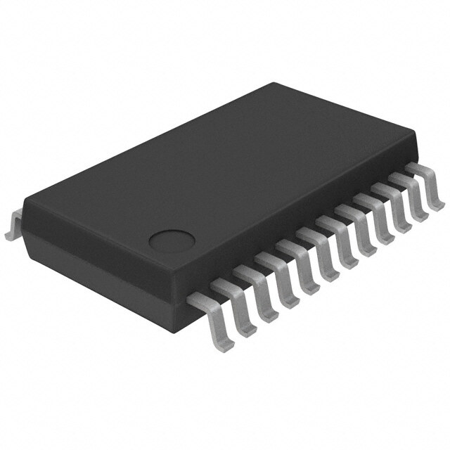
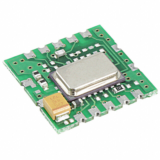
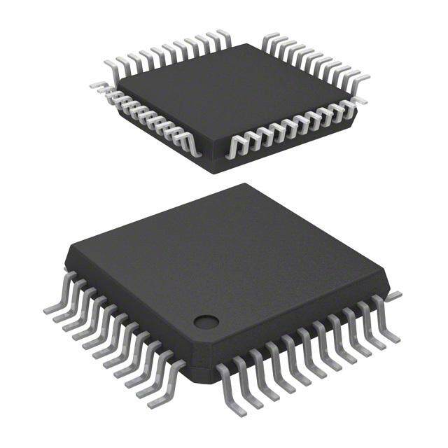
ICGOO在线商城 > 射频/IF 和 RFID > RF 发射器 > TH72036KLD-CAA-000-TU
- 型号: TH72036KLD-CAA-000-TU
- 制造商: MELEXIS
- 库位|库存: xxxx|xxxx
- 要求:
| 数量阶梯 | 香港交货 | 国内含税 |
| +xxxx | $xxxx | ¥xxxx |
查看当月历史价格
查看今年历史价格
TH72036KLD-CAA-000-TU产品简介:
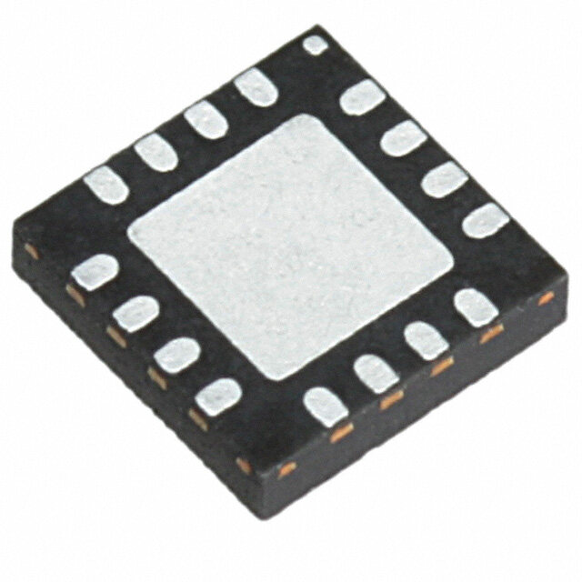
ICGOO电子元器件商城为您提供TH72036KLD-CAA-000-TU由MELEXIS设计生产,在icgoo商城现货销售,并且可以通过原厂、代理商等渠道进行代购。 TH72036KLD-CAA-000-TU价格参考。MELEXISTH72036KLD-CAA-000-TU封装/规格:RF 发射器, RF Transmitter ASK, FSK 868MHz, 915MHz -12dBm ~ 9.5dBm 40kbps PCB, Surface Mount Antenna 10-VFDFN Exposed Pad。您可以下载TH72036KLD-CAA-000-TU参考资料、Datasheet数据手册功能说明书,资料中有TH72036KLD-CAA-000-TU 详细功能的应用电路图电压和使用方法及教程。
| 参数 | 数值 |
| 产品目录 | |
| 描述 | IC XMITTER 868/915MHZ 10QFN |
| 产品分类 | |
| 品牌 | Melexis Technologies NV |
| 数据手册 | http://www.melexis.com/Asset/TH72036-DataSheet-DownloadLink-5050.aspx |
| 产品图片 | |
| 产品型号 | TH72036KLD-CAA-000-TU |
| rohs | 无铅 / 符合限制有害物质指令(RoHS)规范要求 |
| RoHS指令信息 | http://www.melexis.com/Asset/Green--Halogen-Free-Compliance-Declaration-TH72035-DownloadLink-5792.aspx |
| 产品系列 | - |
| 其它名称 | TH72036KLD-TU |
| 功率-输出 | -12dBm ~ 9.5dBm |
| 包装 | 管件 |
| 天线连接器 | PCB,表面贴装 |
| 存储容量 | - |
| 封装/外壳 | 10-VFQFN 裸露焊盘 |
| 工作温度 | -40°C ~ 125°C |
| 应用 | 报警和安全系统,RKE,TPMS |
| 数据接口 | PCB,表面贴装 |
| 数据速率(最大值) | 40kbps |
| 标准包装 | 121 |
| 特性 | - |
| 电压-电源 | 1.95 V ~ 5.5 V |
| 电流-传输 | 5.5mA ~ 13.8mA |
| 调制或协议 | ASK,FSK |
| 频率 | 868MHz,915MHz |


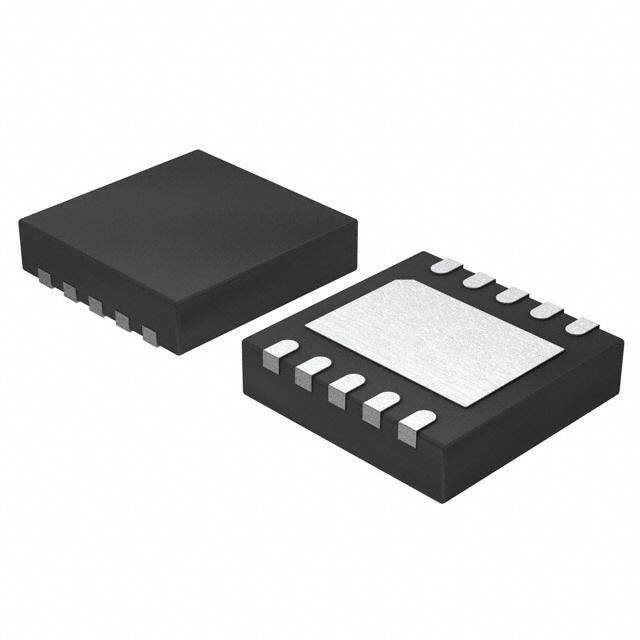
PDF Datasheet 数据手册内容提取
TH72036 868/915MHz FSK/ASK Transmitter Features Application Examples Fully integrated PLL-stabilized VCO Tire Pressure Monitoring System (TPMS) Frequency range from 850 MHz to 930 MHz Remote Keyless Entry (RKE) Single-ended RF output Automatic Meter Reading (AMR) FSK through crystal pulling allows Alarm and security systems modulation from DC to 40 kbit/s Garage door openers High FSK deviation possible for wideband Home and building automation data transmission Low-power telemetry ASK achieved by on/off keying of internal Wireless access control power amplifier up to 40 kbit/s Wide power supply range from 1.95 V to 5.5 Pin Description V Very low standby current Microcontroller clock output On-chip low voltage detector High over-all frequency accuracy FSK deviation and center frequency independently adjustable Adjustable output power range from -13 dBm to +9.5 dBm Adjustable current consumption from 2.5 mA to 20.1 mA Conforms to EN 300 220 and similar standards 10-pin quad flat no lead (QFN) package Ordering information Product Code Temperature Code Package Code Option Code Packing Form Code TH72036 K LD CAA-000 RE TH72036 K LD CAA-000 TU Legend: Temperature Code: K for Temperature Range -40°C to 125°C Package Code: LD for QFN double Packing Form: RE for Reel, TU for Tube Ordering example: TH72036KLD-CAA-000-TU General Description The TH72036 FSK/ASK transmitter IC is designed for applications in the European 868 MHz industrial-scientific-medical (ISM) band, according to the EN 300 220 telecommunications standard. It can also be used for any other system with carrier frequencies ranging from 850 MHz to 930 MHz (e.g. for applications in the US 902 to 928 MHz ISM band). The transmitter's carrier frequency f is determined by the frequency of the reference crystal f . The integrated PLL c ref synthesizer ensures that carrier frequencies, ranging from 850 MHz to 930 MHz, can be achieved. This is done by using a crystal with a reference frequency according to: f = f /N, where N = 32 is the PLL feedback divider ratio. ref c A clock signal with selectable frequency is provided. It can be used to drive a microcontroller. Page 1 of 16 REVISION 010 - JUNE 14, 2017 3901072036
TH72036 868/915MHz FSK/ASK Transmitter Contents Features ..................................................................................................................................................... 1 Application Examples ................................................................................................................................. 1 Pin Description ........................................................................................................................................... 1 Ordering information ................................................................................................................................. 1 General Description ................................................................................................................................... 1 1. Theory of Operation ............................................................................................................................... 4 1.1. General................................................................................................................................................ 4 1.2. Block Diagram ..................................................................................................................................... 4 2. Functional Description ........................................................................................................................... 4 2.1. Crystal Oscillator ................................................................................................................................. 4 2.2. FSK Modulation .................................................................................................................................. 5 2.3. Crystal Pulling ..................................................................................................................................... 5 2.4. ASK Modulation .................................................................................................................................. 6 2.5. Output Power Selection ..................................................................................................................... 6 2.6. Lock Detection .................................................................................................................................... 6 2.7. Low Voltage Detection ....................................................................................................................... 6 2.8. Mode Control Logic ............................................................................................................................ 7 2.9. Clock Output ....................................................................................................................................... 7 2.10. Timing Diagrams ............................................................................................................................... 7 3. Pin Definition and Description ................................................................................................................ 8 4. Electrical Characteristics ........................................................................................................................ 9 4.1. Absolute Maximum Ratings ............................................................................................................... 9 4.2. Normal Operating Conditions ............................................................................................................ 9 4.3. Crystal Parameters ............................................................................................................................. 9 4.4. DC Characteristics ............................................................................................................................ 10 4.5. AC Characteristics ............................................................................................................................. 11 4.6. AC Characteristics ............................................................................................................................. 12 4.7. Output Power Steps – ASK Mode .................................................................................................... 12 5. Test Circuit ........................................................................................................................................... 13 5.1. Test circuit component list to Fig. 6 ................................................................................................ 13 6. Package Description ............................................................................................................................. 14 Page 2 of 16 REVISION 010 - JUNE 14, 2017 3901072036
TH72036 868/915MHz FSK/ASK Transmitter 6.1. Soldering Information ...................................................................................................................... 14 6.2. Recommended PCB Footprints ........................................................................................................ 14 7. Standard information regarding manufacturability of Melexis products with different soldering processes ............................................................................................................................. 15 8. ESD Precautions ................................................................................................................................... 15 9. Contact................................................................................................................................................. 16 10. Disclaimer .......................................................................................................................................... 16 Page 3 of 16 REVISION 010 - JUNE 14, 2017 3901072036
TH72036 868/915MHz FSK/ASK Transmitter 1. Theory of Operation 1.1. General As depicted in Fig.1, the TH72036 transmitter consists of a fully integrated voltage-controlled oscillator (VCO), a divide-by-32 divider (div32), a phase-frequency detector (PFD) and a charge pump (CP). An internal loop filter determines the dynamic behavior of the PLL and suppresses reference spurious signals. A Colpitts crystal oscillator (XOSC) is used as the reference oscillator of a phase-locked loop (PLL) synthesizer. The VCO’s output signal feeds the power amplifier (PA). The RF signal power P can be adjusted in four steps from P = –11 dBm to +9.5 dBm, either out out by changing the value of resistor RPSor by varying the voltage V at pin PSEL. The open-collector output (OUT) can be PS used either to directly drive a loop antenna or to be matched to a 50Ohm load. Bandgap biasing ensures stable operation of the IC at a power supply range of 1.95 V to 5.5 V. 1.2. Block Diagram RPS R1 ASKDTA CKDIV VCC PSEL 7 10 6 PLL CKOUT div 8 antenna 5 div 32 32 PA 8 OUT matching network ROI PFD 3 XOSC XBUF XTAL CP VCO mode 4 ENTX control FSKSW CX2 2 CX1 1 9 FSKDTA VEE Fig. 1: Block diagram with external components 2. Functional Description 2.1. Crystal Oscillator A Colpitts crystal oscillator with integrated functional capacitors is used as the reference oscillator for the PLL synthesizer. The equivalent input capacitance CRO offered by the crystal oscillator input pin ROI is about 18pF. The crystal oscillator is provided with an amplitude control loop in order to have a very stable frequency over the specified supply voltage and temperature range in combination with a short start-up time. Page 4 of 16 REVISION 010 - JUNE 14, 2017 3901072036
TH72036 868/915MHz FSK/ASK Transmitter 2.2. FSK Modulation FSK modulation can be achieved by pulling the VCC crystal oscillator frequency. A CMOS-compatible Fig. 2: Crystal pulling circuitry data stream applied at the pin FSKDTA digitally ROI modulates the XOSC via an integrated NMOS switch. Two external pulling capacitors CX1 and CX2 XTAL allow the FSK deviation f and the center frequency FSKSW f to be adjusted independently. At FSKDTA = 0, CX2 c is connected in parallel to CX1 leading to the low- CX2 frequency component of the FSK spectrum (f ); CX1 min while at FSKDTA = 1, CX2 is deactivated and the VEE XOSC is set to its high frequency f . max An external reference signal can be directly AC- coupled to the reference oscillator input pin ROI. Then the transmitter is used without a crystal. Now FSKDTA Description the reference signal sets the carrier frequency and may also contain the FSK (or FM) modulation. 0 f = f - f (FSK switch is closed) min c 1 f = f + f (FSK switch is open) max c 2.3. Crystal Pulling A crystal is tuned by the manufacturer to the f required oscillation frequency f at a given load 0 capacitance CL and within the specified calibration tolerance. The only way to pull the oscillation XTAL frequency is to vary the effective load capacitance CLeff seen by the crystal. L1 Figure 3 shows the oscillation frequency of a crystal fmax as a function of the effective load capacitance. This C1 C0 CLeff capacitance changes in accordance with the logic R1 level of FSKDTA around the specified load fc capacitance. The figure illustrates the relationship between the external pulling capacitors and the frequency deviation. fmin It can also be seen that the pulling sensitivity increases with the reduction of CL. Therefore, applications with a high frequency deviation require a low load capacitance. For narrow band FSK CLeff applications, a higher load capacitance could be CX1 CRO CL (CX1+CX2) CRO CX1+CRO CX1+CX2+CRO chosen in order to reduce the frequency drift caused by the tolerances of the chip and the external pulling capacitors. Fig. 3: Crystal pulling characteristic For ASK applications CX2 can be omitted. Then CX1 has to be adjusted for center frequency. Page 5 of 16 REVISION 010 - JUNE 14, 2017 3901072036
TH72036 868/915MHz FSK/ASK Transmitter 2.4. ASK Modulation The TH72036 can be ASK-modulated by applying data directly at pin PSEL. This turns the PA on and off which leads to an ASK signal at the output. 2.5. Output Power Selection The transmitter is provided with an output power selection feature. There are four predefined output power steps and one off-step accessible via the power selection pin PSEL. A digital power step adjustment was chosen because of its high accuracy and stability. The number of steps and the step sizes as well as the corresponding power levels are selected to cover a wide spectrum of different applications. The implementation of the output power control logic is shown in figure 4. There are two matched current sources with an amount of about 8 µA. One current source is directly applied to the PSEL pin. RPS The other current source is used for the generation of reference voltages with a resistor ladder. These PSEL reference voltages are defining the thresholds between the power steps. The four comparators & deliver thermometer-coded control signals depending on the voltage level at the pin PSEL. In & & & & order to have a certain amount of ripple tolerance in a noisy environment the comparators are provided with a little hysteresis of about 20 mV. With these control signals, weighted current sources of the power amplifier are switched on or OUT off to set the desired output power level (Digitally Controlled Current Source). The LOCK, ASK signal and the output of the low voltage detector are Fig. 4: Block diagram of output power control circuitry gating this current source. There are two ways to select the desired output power step. First by applying a DC voltage at the pin PSEL, then this voltage directly selects the desired output power step. This kind of power selection can be used if the transmission power must be changed during operation. For a fixed-power application a resistor can be used which is connected from the PSEL pin to ground. The voltage drop across this resistor selects the desired output power level. For fixed- power applications at the highest power step this resistor can be omitted. The pin PSEL is in a high impedance state during the “TX standby” mode. 2.6. Lock Detection The lock detection circuitry turns on the power amplifier only after PLL lock. This prevents from unwanted emission of the transmitter if the PLL is unlocked. 2.7. Low Voltage Detection The supply voltage is sensed by a low voltage detect circuitry. The power amplifier is turned off if the supply voltage drops below a value of about 1.85 V. This is done in order to prevent unwanted emission of the transmitter if the supply voltage is too low. Page 6 of 16 REVISION 010 - JUNE 14, 2017 3901072036
TH72036 868/915MHz FSK/ASK Transmitter 2.8. Mode Control Logic The mode control logic allows two different modes EN Mode Description of operation as listed in the following table. The 0 TX standby TX disabled mode control pin EN is pulled-down internally. This guarantees that the whole circuit is shut down if 1 TX active TX / CKOUT this pin is left floating. CKOUT active enabled 2.9. Clock Output The clock output CKOUT is CMOS-compatible and can be used to drive a microcontroller. The frequency of the clock can be selected by the clock divider control signal CKDIV, according to the following table. A capacitor at pin CKOUT can be used to control the clock voltage swing and the RF spurious emission. CKDIV Clock divider ratio Clock frequency / f=868.3MHz c 0 8 3.39MHz 1 32 848kHz 2.10. Timing Diagrams After enabling the transmitter by the EN signal, the power amplifier remains inactive for the time t , the transmitter on start-up time. The crystal oscillator starts oscillation and the PLL locks to the desired output frequency within the time duration t . After successful PLL lock, the LOCK signal turns on the power amplifier, and then the RF carrier can be FSK on or ASK modulated. high high EN EN low low high high LOCK LOCK low low high high FSKDTA PSEL low low RF carrier t t t t on on Fig. 5: Timing diagrams for FSK and ASK modulation Page 7 of 16 REVISION 010 - JUNE 14, 2017 3901072036
TH72036 868/915MHz FSK/ASK Transmitter 3. Pin Definition and Description Pin No. Name I/O Type Functional Schematic Description 1 FSKDTA input 0: ENTX=1 FSK data input, 1: ENTX=0 CMOS compatible with internal FSKDTA 1.5k pull-up circuit 1 TX standby: no pull-up TX active: pull-up 2 FSKSW analog I/O XOSC FSK pulling pin, MOS switch FSKSW 2 3 ROI analog I/O XOSC connection to XTAL, Colpitts type crystal oscillator 25k ROI 3 36p 36p 4 EN input mode control input, CMOS-compatible with EN 1.5k internal pull-down circuit 4 5 CKOUT output clock output, CMOS-compatible CKOUT 400 5 6 PSEL analog I/O power select input, high- 8µA impedance comparator logic PSEL 1.5k TX standby: I = 0 6 PSEL TX active: I = 8µA PSEL 7 CKDIV input clock divider control input, CMOS compatible with internal CKDIV 1.5k pull-down circuit 7 TX standby: no pull-down 0: ENTX=0 1: ENTX=1 TX active: pull-down 8 OUT output OUT VCC power amplifier output, open collector 8 VEE VEE 9 VEE ground negative power supply 10 VCC supply positive power supply Page 8 of 16 REVISION 010 - JUNE 14, 2017 3901072036
TH72036 868/915MHz FSK/ASK Transmitter 4. Electrical Characteristics 4.1. Absolute Maximum Ratings Parameter Symbol Condition Min Max Unit Supply voltage V 0 7.0 V CC Input voltage V -0.3 V +0.3 V IN CC Storage temperature T -65 150 °C STG Junction temperature T 150 °C J Thermal Resistance R 49 K/W thJA Power dissipation P 0.12 W diss Electrostatic discharge V human body model (HBM) 2.0 kV ESD according to CDF-AEC-Q100- 002 4.2. Normal Operating Conditions Parameter Symbol Condition Min Max Unit Supply voltage V 1.95 5.5 V CC Operating temperature T -40 125 °C A Input low voltage CMOS V EN, FSKDTA 0.3*V V IL CC Input high voltage CMOS V EN, FSKDTA 0.7*V V IH CC XOSC frequency f set by the crystal 26.6 29 MHz ref VCO frequency f f = 32 f 850 930 MHz c c ref Clock frequency f CKDIV=0, f = f / 8 3.3 3.6 MHz CLK CLK ref CKDIV=1, f = f / 32 831 906 kHz CLK ref FSK deviation f depending on CX1, CX2 and 2.5 40 kHz crystal parameters FSK Data rate R NRZ 40 kbit/s ASK Data rate R NRZ 40 kbit/s 4.3. Crystal Parameters Parameter Symbol Condition Min Max Unit Crystal frequency f fundamental mode, AT 26.6 29 MHz 0 Load capacitance C 10 15 pF L Static capacitance C 7 pF 0 Series resistance R 50 1 Spurious response a only required for FSK -10 dB spur Page 9 of 16 REVISION 010 - JUNE 14, 2017 3901072036
TH72036 868/915MHz FSK/ASK Transmitter 4.4. DC Characteristics all parameters under normal operating conditions, unless otherwise stated; typical values at T = 23 °C and V = 3 V A CC Parameter Symbol Condition Min Typ Max Unit Operating Currents Standby current EN=0, T =85°C 0.2 200 nA I A SBY EN=0, T =125°C 4 µA A Supply current in power step 0 I EN=1 2.5 4.3 7.4 mA CC0 Supply current in power step 1 I EN=1 3.5 5.5 9.4 mA CC1 Supply current in power step 2 I EN=1 4.5 6.8 11.1 mA CC2 Supply current in power step 3 I EN=1 6.2 9.0 13.8 mA CC3 Supply current in power step 4 I EN=1 9.4 13.8 20.1 mA CC4 Digital Pin Characteristics Input low voltage CMOS V EN, FSKDTA -0.3 0.3*V V IL cc Input high voltage CMOS V EN, FSKDTA 0.7*V V +0.3 V IH CC CC Pull down current, EN I EN=1 0.2 4.0 40 µA PDEN Low level input current, EN I EN=0 0.02 µA INLEN High level input current, FSKDTA I FSKDTA=1 0.02 µA INHDTA Pull up current FSKDTA I FSKDTA=0, EN=1 0.1 1.5 12 µA PUDTAa active mode Pull up current FSK I FSKDTA=0, EN=0 0.02 µA PUDTAs standby mode Low level input current CKDIV I CKDIV=0 0.02 µA INLCKDIV Pull-down current CKDIV I CKDIV=1, EN=1 0.1 1.5 12 µA PDCKDIVa active mode Pull-down current CKDIV I CKDIV=1, EN=0 0.02 µA PDCKDIVs standby mode FSK Switch Resistance MOS switch On resistance R FSKDTA=0, EN=1 20 70 ON MOS switch Off resistance R FSKDTA=1, EN=1 1 M OFF Power Select Characteristics Power select current I EN=1 7.0 8.6 9.9 µA PSEL Power select voltage step 0 V EN=1 0.035 V PS0 Power select voltage step 1 V EN=1 0.14 0.24 V PS1 Power select voltage step 2 V EN=1 0.37 0.60 V PS2 Power select voltage step 3 V EN=1 0.78 1.29 V PS3 Power select voltage step 4 V EN=1 1.55 V PS4 Low Voltage Detection Characteristic Low voltage detect threshold V EN=1 1.75 1.85 1.95 V LVD Page 10 of 16 REVISION 010 - JUNE 14, 2017 3901072036
TH72036 868/915MHz FSK/ASK Transmitter 4.5. AC Characteristics all parameters under normal operating conditions, unless otherwise stated; typical values at T = 23 °C and V = 3 V; test circuit shown in Fig. 6, f = 868.3MHz A CC c Parameter Symbol Condition Min Typ Max Unit CW Spectrum Characteristics Output power in step 0 P EN=1 -70 dBm off (Isolation in off-state) Output power in step 1 P EN=1 -13 -12 -11 1) dBm 1 Output power in step 2 P EN=1 -4 -3 -2 1) dBm 2 Output power in step 3 P EN=1 1 2.5 3.5 1) dBm 3 Output power in step 4 P EN=1 4 7.5 9.5 1) dBm 4 Phase noise L(f ) @ 200kHz offset -87 -82 dBc/Hz m Spurious emissions according P 47MHz< f <74MHz -54 dBm spur to EN 300 220-1 (2000.09) 87.5MHz< f <118MHz table 13 174MHz< f <230MHz 470MHz< f <862MHz B=100kHz f < 1GHz, B=100kHz -36 dBm f > 1GHz, B=1MHz -30 dBm Clock output Characteristics Output low voltage CMOS V depending on capacitor 0.3*V V OL CC CCK Output high voltage CMOS V 0.7*V V OH CC and CKDIV Start-up Parameters Start-up time t from standby to 0.6 1 ms on transmit mode Frequency Stability Frequency stability vs. supply df 3 ppm VCC voltage Frequency stability vs. df crystal at constant 10 ppm TA temperature temperature Frequency stability vs. df 20 ppm CRO variation range of C RO 1) output matching network tuned for 5V supply Page 11 of 16 REVISION 010 - JUNE 14, 2017 3901072036
TH72036 868/915MHz FSK/ASK Transmitter 4.6. AC Characteristics Power step 0 1 2 3 4 RPS / k < 3 22 56 120 not connected 4.7. Output Power Steps – ASK Mode typical values at T = 23 °C and V = 3 V; test circuit shown in Fig. 6 A CC Power step 1 2 3 4 RPS / k 2.4 2.8 3.5 not connected R1 / k 36 14 7 0 VPSlow V = voltage across RPS if ASK_DTA at 0V RPS R1 RPS PSlow V V = voltage across RPS if ASK_DTA at Vcc PShigh R1 PShigh Vcc PSEL 6 PSEL 6 If the transmitter is operated at any supply voltage V , the values for R1 and RPS can be calculated as follows: cc V V V R CC PSlow R R PShigh 1 I V PS 1V V PSEL PShigh CC PShigh Page 12 of 16 REVISION 010 - JUNE 14, 2017 3901072036
TH72036 868/915MHz FSK/ASK Transmitter 5. Test Circuit CM2 CM1 RPS LM OUT CM3 LT CB1 10 9 8 7 6 C E T V L VC VE OU KDI PSE C DTA SW UT SK SK OI N KO F F R E C 1 2 3 4 5 2 X K C L C A C T R1 CX1 X CB0 1 2 1 2 1 2 3 1 2 1 2 1 2 DC DA CND DA CV TD GNVC GNSK_DT VCEGN GNSK_DT VCCKDI CKOUGN F A Fig. 6: Test circuit for FSK and ASK with 50 matching network 5.1. Test circuit component list to Fig. 6 Part Size Value @ Value @ Tolerance Description 868.3 MHz 915 MHz CM1 0805 1.8 pF 2.2 pF 5% impedance matching capacitor CM2 0805 5.6 pF 5.6 pF 5% impedance matching capacitor CM3 0805 68 pF 68 pF 5% impedance matching capacitor LM 0805 12 nH 10 nH 5% impedance matching inductor, note 2 LT 0805 15 nH 10 nH 5% output tank inductor, note 2 CX1 0805 22 pF 22 pF 5% XOSC FSK capacitor (f = 20 kHz), note 1 _FSK CX1 0805 27 pF 27 pF 5% XOSC ASK capacitor, trimmed to f , note 1 _ASK C CX2 0805 12 pF 12 pF 5% XOSC capacitor (f = 20 kHz), note 1 only needed for FSK CCK 0805 15 pF / 180 pF 5% clock spur suppression capacitor, CKDIV 0 / 1 RPS 0805 see section 4.6 5% FSK or CW mode power-select resistor R1 see section 4.7 ASK power-select resistor, not used at FSK CB0 0805 220 nF 20% de-coupling capacitor CB1 0805 330 pF 10% de-coupling capacitor XTAL SMD 27.13438 MHz 28.59375 MHz 30ppm calibr. fundamental wave crystal, 6x3.5 30ppm temp. CL = 12 pF, C0, max = 7 pF, R1 = 40 Note 1: value depending on crystal parameters Note 2: for high-power applications high-Q wire-wound inductors should be used Page 13 of 16 REVISION 010 - JUNE 14, 2017 3901072036
TH72036 868/915MHz FSK/ASK Transmitter 6. Package Description The device TH72036 is RoHS compliant. D D2 10 6 L 0.23 exposed pad 0.36 E E2 0.225x45° 1 5 b e A3 A Exposed pad not connected to internal GND. It should not be connected to the PCB. A1 It can be with or without fingers. Fig. 7: 10L QFN 3x3 Dual all Dimensions in mm D E D2 E2 A A1 A3 L e b min 2.85 2.85 2.23 1.49 0.80 0 0.3 0.18 0.20 0.50 max 3.15 3.15 2.48 1.74 1.00 0.05 0.5 0.30 all Dimensions in inch min 0.112 0.112 0.0878 0.051 0.0315 0 0.0118 0.0071 0.0079 0.0197 max 0.124 0.124 0.0976 0.055 0.0393 0.002 0.0197 0.0118 6.1. Soldering Information The device TH72036 is qualified for MSL1 with soldering peak temperature 260 deg C according to JEDEC J-STD-20 6.2. Recommended PCB Footprints X e all Dimensions in mm C Y PL Z G D2 E2 X Y C e th th PL 10 6 min 3.55 1.9 3.2 1.3 0.25 0.7 0.3 0.5 Z G E2 max 3.90 2.3 3.6 1.7 0.30 1.0 0.5 th all Dimensions in inch 1 5 min 0.1398 0.0748 0.1260 0.0512 0.0098 0.0276 0.0591 0.0197 max 0.1535 0.0906 0.1417 0.0669 0.0118 0.0394 0.0197 D2 th solder pad solder stop Fig. 8: PCB land pattern style Page 14 of 16 REVISION 010 - JUNE 14, 2017 3901072036
TH72036 868/915MHz FSK/ASK Transmitter 7. Standard information regarding manufacturability of Melexis products with different soldering processes Our products are classified and qualified regarding soldering technology, solderability and moisture sensitivity level according to following test methods: Reflow Soldering SMD’s (Surface Mount Devices) IPC/JEDEC J-STD-020 Moisture/Reflow Sensitivity Classification for Nonhermetic Solid State Surface Mount Devices (classification reflow profiles according to table 5-2) EIA/JEDEC JESD22-A113 Preconditioning of Nonhermetic Surface Mount Devices Prior to Reliability Testing (reflow profiles according to table 2) Wave Soldering SMD’s (Surface Mount Devices) and THD’s (Through Hole Devices) EN60749-20 Resistance of plastic- encapsulated SMD’s to combined effect of moisture and soldering heat EIA/JEDEC JESD22-B106 and EN60749-15 Resistance to soldering temperature for through-hole mounted devices Iron Soldering THD’s (Through Hole Devices) EN60749-15 Resistance to soldering temperature for through-hole mounted devices Solderability SMD’s (Surface Mount Devices) and THD’s (Through Hole Devices) EIA/JEDEC JESD22-B102 and EN60749-21 Solderability For all soldering technologies deviating from above mentioned standard conditions (regarding peak temperature, temperature gradient, temperature profile etc) additional classification and qualification tests have to be agreed upon with Melexis. The application of Wave Soldering for SMD’s is allowed only after consulting Melexis regarding assurance of adhesive strength between device and board. Melexis is contributing to global environmental conservation by promoting lead free solutions. For more information on qualifications of RoHS compliant products (RoHS = European directive on the Restriction Of the use of certain Hazardous Substances) please visit the quality page on our website: http://www.melexis.com/quality.aspx 8. ESD Precautions Electronic semiconductor products are sensitive to Electro Static Discharge (ESD). Always observe Electro Static Discharge control procedures whenever handling semiconductor products. REVISION 010 - JUNE 14, 2017 Page 15 of 16 3901072036
TH72036 868/915MHz FSK/ASK Transmitter 9. Contact For the latest version of this document, go to our website at www.melexis.com. For additional information, please contact our Direct Sales team and get help for your specific needs: Europe, Africa Telephone: +32 13 67 04 95 Email : sales_europe@melexis.com Americas Telephone: +1 603 223 2362 Email : sales_usa@melexis.com Asia Email : sales_asia@melexis.com 10. Disclaimer The information furnished by Melexis herein (“Information”) is believed to be correct and accurate. Melexis disclaims (i) any and all liability in connection with or arising out of the furnishing, performance or use of the technical data or use of the product(s) as described herein (“Product”) (ii) any and all liability, including without limitation, special, consequential or incidental damages, and (iii) any and all warranties, express, statutory, implied, or by description, including warranties of fitness for particular purpose, non- infringement and merchantability. No obligation or liability shall arise or flow out of Melexis’ rendering of technical or other services. The Information is provided "as is” and Melexis reserves the right to change the Information at any time and without notice. Therefore, before placing orders and/or prior to designing the Product into a system, users or any third party should obtain the latest version of the relevant information to verify that the information being relied upon is current. Users or any third party must further determine the suitability of the Product for its application, including the level of reliability required and determine whether it is fit for a particular purpose. The Information is proprietary and/or confidential information of Melexis and the use thereof or anything described by the Information does not grant, explicitly or implicitly, to any party any patent rights, licenses, or any other intellectual property rights. This document as well as the Product(s) may be subject to export control regulations. Please be aware that export might require a prior authorization from competent authorities. The Product(s) are intended for use in normal commercial applications. Unless otherwise agreed upon in writing, the Product(s) are not designed, authorized or warranted to be suitable in applications requiring extended temperature range and/or unusual environmental requirements. High reliability applications, such as medical life-support or life- sustaining equipment are specifically not recommended by Melexis. The Product(s) may not be used for the following applications subject to export control regulations: the development, production, processing, operation, maintenance, storage, recognition or proliferation of 1) chemical, biological or nuclear weapons, or for the development, production, maintenance or storage of missiles for such weapons: 2) civil firearms, including spare parts or ammunition for such arms; 3) defense related products, or other material for military use or for law enforcement; 4) any applications that, alone or in combination with other goods, substances or organisms could cause serious harm to persons or goods and that can be used as a means of violence in an armed conflict or any similar violent situation. The Products sold by Melexis are subject to the terms and conditions as specified in the Terms of Sale, which can be found at https://www.melexis.com/en/legal/terms-and- conditions. This document supersedes and replaces all prior information regarding the Product(s) and/or previous versions of this document. Melexis NV © - No part of this document may be reproduced without the prior written consent of Melexis. (2016) ISO/TS 16949 and ISO14001 Certified REVISION 010 - JUNE 14, 2017 Page 16 of 16 3901072036
 Datasheet下载

