ICGOO在线商城 > TDE1898CDP
 Datasheet下载
- 型号: TDE1898CDP
- 制造商: STMicroelectronics
- 库位|库存: xxxx|xxxx
- 要求:
| 数量阶梯 | 香港交货 | 国内含税 |
| +xxxx | $xxxx | ¥xxxx |
查看当月历史价格
查看今年历史价格
TDE1898CDP产品简介:
ICGOO电子元器件商城为您提供TDE1898CDP由STMicroelectronics设计生产,在icgoo商城现货销售,并且可以通过原厂、代理商等渠道进行代购。 提供TDE1898CDP价格参考以及STMicroelectronicsTDE1898CDP封装/规格参数等产品信息。 你可以下载TDE1898CDP参考资料、Datasheet数据手册功能说明书, 资料中有TDE1898CDP详细功能的应用电路图电压和使用方法及教程。
| 参数 | 数值 |
| 产品目录 | 集成电路 (IC) |
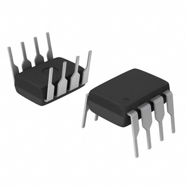
| 描述 | IC IPS HISIDE DRVR 0.5A 8-DIP |
| 产品分类 | PMIC - MOSFET,电桥驱动器 - 内部开关 |
| 品牌 | STMicroelectronics |
| 数据手册 | |
| 产品图片 |
|
| 产品型号 | TDE1898CDP |
| rohs | 无铅 / 符合限制有害物质指令(RoHS)规范要求 |
| 产品系列 | - |
| 产品目录页面 | |
| 供应商器件封装 | 8-迷你型 DIP |
| 其它名称 | 497-5425-5 |
| 包装 | 管件 |
| 安装类型 | 通孔 |
| 导通电阻 | - |
| 封装/外壳 | 8-DIP(0.200",5.08mm) |
| 工作温度 | -25°C ~ 85°C |
| 标准包装 | 50 |
| 电压-电源 | 18 V ~ 35 V |
| 电流-峰值输出 | 1.5A |
| 电流-输出/通道 | 500mA |
| 类型 | 高端 |
| 输入类型 | 差分 |
| 输出数 | 1 |


- 商务部:美国ITC正式对集成电路等产品启动337调查
- 曝三星4nm工艺存在良率问题 高通将骁龙8 Gen1或转产台积电
- 太阳诱电将投资9.5亿元在常州建新厂生产MLCC 预计2023年完工
- 英特尔发布欧洲新工厂建设计划 深化IDM 2.0 战略
- 台积电先进制程称霸业界 有大客户加持明年业绩稳了
- 达到5530亿美元!SIA预计今年全球半导体销售额将创下新高
- 英特尔拟将自动驾驶子公司Mobileye上市 估值或超500亿美元
- 三星加码芯片和SET,合并消费电子和移动部门,撤换高东真等 CEO
- 三星电子宣布重大人事变动 还合并消费电子和移动部门
- 海关总署:前11个月进口集成电路产品价值2.52万亿元 增长14.8%


PDF Datasheet 数据手册内容提取
TDE1897C TDE1898C ® 0.5A HIGH-SIDE DRIVER INDUSTRIAL INTELLIGENT POWER SWITCH 0.5A OUTPUT CURRENT MULTIPOWER BCD TECHNOLOGY 18V TO 35V SUPPLY VOLTAGE RANGE INTERNAL CURRENT LIMITING THERMAL SHUTDOWN OPEN GROUND PROTECTION INTERNAL NEGATIVE VOLTAGE CLAMPING TO V - 45V FOR FAST DEMAGNETIZATION S DIFFERENTIAL INPUTS WITH LARGE COM- Minidip SIP9 SO20 MON MODE RANGE AND THRESHOLD HYSTERESIS ORDERING NUMBERS: UNDERVOLTAGE LOCKOUT WITH HYSTERESIS TDE1897CDP TDE1898CSP TDE1897CFP OPEN LOAD DETECTION TDE1898CDP TDE1898CFP TWO DIAGNOSTIC OUTPUTS ogy, for driving inductive or resistive loads. An in- OUTPUT STATUS LED DRIVER ternal Clamping Diode enables the fast demag- netization of inductive loads. Diagnostic for CPU feedback and extensive use DESCRIPTION of electrical protections make this device inher- The TDE1897C/TDE1898C is a monolithic Intelli- ently indistructible and suitable for general pur- gent Power Switch in Multipower BCD Technol- pose industrial applications. BLOCK DIAGRAM September 2003 1/12
TDE1897C - TDE1898C PIN CONNECTIONS (Top view) Minidip SO20 SIP9 ABSOLUTE MAXIMUM RATINGS (Minidip pin reference) Symbol Parameter Value Unit VS Supply Voltage (Pins 3 - 1) (TW < 10ms) 50 V VS – VO Supply to Output Differential Voltage. See also VCl 3-2 (Pins 3 - 2) internally limited V Vi Input Voltage (Pins 7/8) -10 to VS +10 V Vi Differential Input Voltage (Pins 7 - 8) 43 V Ii Input Current (Pins 7/8) 20 mA IO Output Current (Pins 2 - 1). See also ISC internally limited A El Energy from Inductive Load (TJ = 85(cid:176) C) 200 mJ Ptot Power Dissipation. See also THERMAL CHARACTERISTICS. internally limited W Top Operating Temperature Range (Tamb) -25 to +85 (cid:176) C Tstg Storage Temperature -55 to 150 (cid:176) C THERMAL DATA Symbol Description Minidip Sip SO20 Unit Rth j-case Thermal Resistance Junction-case Max. 10 (cid:176) C/W Rth j-amb Thermal Resistance Junction-ambient Max. 100 70 90 (cid:176) C/W 2/12
TDE1897C - TDE1898C ELECTRICAL CHARACTERISTICS (VS = 24V; Tamb = –25 to +85°C, unless otherwise specified) Symbol Parameter Test Condition Min. Typ. Max. Unit Vsmin 3 Supply Voltage for Valid Idiag > 0.5mA @ Vdg1 = 1.5V 9 35 V Diagnostics Vs 3 Supply Voltage (operative) 18 24 35 V Iq 3 Quiescent Current Vil 2.5 4 mA Iout = Ios = 0 Vih 4.5 7.5 mA Vsth1 Undervoltage Threshold 1 (See fig. 1); Tamb = 0 to +85(cid:176) C 11 V Vsth2 3 Undervoltage Threshold 2 (See fig. 1); Tamb = 0 to +85(cid:176) C 15.5 V Vshys Supply Voltage Hysteresis (See fig. 1); Tamb = 0 to +85(cid:176) C 0.4 1 3 V Isc Short Circuit Current VS = 18 to 35V; RL = 1W 0.75 1.5 A Vdon 3-2 Output Voltage Drop @ Iout = 625mA; Tj = 25(cid:176) C 250 425 mV @ Iout = 625mA; Tj = 125(cid:176) C 400 600 mV Ioslk 2 Output Leakage Current @ Vi = Vil , Vo = 0V 300 m A ¥ Vol 2 Low State Out Voltage @ Vi = Vil; RL = 0.8 1.5 V Vcl 3-2 Internal Voltage Clamp (VS - VO) @ IO = -500mA 45 55 V Iold 2 Open Load Detection Current Vi = Vih; Tamb = 0 to +85(cid:176) C 1 6 mA Vid 7-8 Common Mode Input Voltage VS = 18 to 35V, –7 15 V Range (Operative) VS = Vid 7-8 < 37V Iib 7-8 Input Bias Current Vi = –7 to 15V; –In = 0V –700 700 m A Vith 7-8 Input Threshold Voltage V+In > V–In 0.8 1.4 2 V Viths 7-8 Input Threshold Hysteresis V+In > V–In 50 400 mV Voltage Rid 7-8 Diff. Input Resistance @ 0 < +In < +16V; –In = 0V 400 KW @ –7 < +In < 0V; –In = 0V 150 KW Iilk 7-8 Input Offset Current V+In = V–In +Ii –20 +20 m A 0V < Vi <5.5V –Ii –75 –25 m A –In = GND +Ii +10 +50 m A 0V < V+In <5.5V –Ii –250 –125 m A +In = GND +Ii –100 –30 m A 0V < V–In <5.5V –Ii –50 –15 m A Voth1 2 Output Status Threshold 1 (See fig. 1) 12 V Voltage Voth2 2 Output Status Threshold 2 (See fig. 1) 9 V Voltage Vohys 2 Output Status Threshold (See fig. 1) 0.3 0.7 2 V Hysteresis Iosd 4 Output Status Source Current Vout > Voth1, Vos = 2.5V 2 4 mA Vosd 3-4 Active Output Status Driver Vs – Vos @ Ios = 2mA; 5 V Drop Voltage Tamb = -25 to 85(cid:176) C Ioslk 4 Output Status Driver Leakage Vout < Voth2 , Vos = 0V 25 m A Current VS = 18 to 35V Vdgl 5/6 Diagnostic Drop Voltage D1 / D2 = L @ Idiag = 0.5mA 250 mV D1 / D2 = L @ Idiag = 3mA 1.5 V Idglk 5/6 Diagnostic Leakage Current D1 / D2 =H @ 0 < Vdg < Vs 25 m A VS = 15.6 to 35V Vfdg 5/6-3 Clamping Diodes at the @ Idiag = 5mA; D1 / D2 = H 2 V Diagnostic Outputs. Voltage Drop to VS Note Vil < 0.8V, Vih > 2V @ (V+In > V–In); Minidip pin reference. All test not dissipative. 3/12
TDE1897C - TDE1898C SOURCE DRAIN NDMOS DIODE Symbol Parameter Test Condition Min. Typ. Max. Unit Vfsd 2-3 Forward On Voltage @ Ifsd = 625mA 1 1.5 V Ifp 2-3 Forward Peak Current t = 10ms; d = 20% 2 A trr 2-3 Reverse Recovery Time If = 625mA di/dt = 25A/m s 200 ns tfr 2-3 Forward Recovery Time 50 ns THERMAL CHARACTERISTICS (*) Q Lim Junction Temp. Protect. 135 150 (cid:176) C TH Thermal Hysteresis 30 (cid:176) C SWITCHING CHARACTERISTICS (VS = 24V; RL = 48W ) (*) ton Turn on Delay Time 100 m s toff Turn off Delay Time 20 m s td Input Switching to Diagnostic 100 m s Valid Note Vil < 0.8V, Vih > 2V @ (V+In > V–In); Minidip pin reference. (*) Not tested. Figure 1 DIAGNOSTIC TRUTH TABLE Diagnostic Conditions Input Output Diag1 Diag2 Normal Operation L L H H H H H H Open Load Condition (Io < Iold) L L H H H H L H Short to VS L H L H H H L H Short Circuit to Ground (IO = ISC) (**) TDE1897C H <H (*) H L H H H H TDE1898C L H H Output DMOS Open L L H H H L L H Overtemperature L L H L H L H L Supply Undervoltage (VS < Vsth1 in the falling phase of the sup- L L L L ply voltage; VS < Vsth2 in the rising phase of the supply voltage) H L L L (*) According to the intervention of the current limiting block. (**) A cold lamp filament, or a capacitive load may activate the current limiting circuit of the IPS, when the IPS is initially turned on. TDE1897 uses Diag2 to signal such condition, TDE1898 does not. 4/12
TDE1897C - TDE1898C APPLICATION INFORMATION Figure 3: Demagnetization Cycle Waveforms DEMAGNETIZATION OF INDUCTIVE LOADS An internal zener diode, limiting the voltage across the Power MOS to between 45 and 55V (Vcl), provides safe and fast demagnetization of inductive loads without external clamping devices. The maximum energy that can be absorbed from an inductive load is specified as 200mJ (at Tj = 85(cid:176) C). To define the maximum switching frequency three points have to be considered: 1) The total power dissipation is the sum of the On State Power and of the Demagnetization Energy multiplied by the frequency. 2) The total energy W dissipated in the device during a demagnetization cycle (figg. 2, 3) is: W = V L [I – Vcl – Vs log (cid:230)(cid:231) 1 + Vs (cid:246)(cid:247) ] cl o RL RL Ł Vcl – Vsł Where: Vcl = clamp voltage; L = inductive load; RL = resistive load; Vs = supply voltage; IO = ILOAD 3) In normal conditions the operating Junction temperature should remain below 125(cid:176) C. Figure 2: Inductive Load Equivalent Circuit Figure 4: Normalized RDSON vs. Junction Temperature D93IN018 a 1.8 RDSON (Tj) a = 1.6 RDSON (Tj=25˚C) 1.4 1.2 1.0 0.8 0.6 -25 0 25 50 75 100 125 Tj (˚C) 5/12
TDE1897C - TDE1898C the third element are constant, while the first WORST CONDITION POWER DISSIPATION IN one increases with temperature because THE ON-STATE RDSON increases as well. In IPS applications the maximum average power dissipation occurs when the device stays for a long time in the ON state. In such a situation the 3) The chip temperature must not exceed Q Lim internal temperature depends on delivered cur- in order do not lose the control of the device. rent (and related power), thermal characteristics The heat dissipation path is represented by of the package and ambient temperature. the thermal resistance of the system device- At ambient temperature close to upper limit board-ambient (Rth). In steady state condi- tions, this parameter relates the power dissi- (+85°C) and in the worst operating conditions, it is possible that the chip temperature could increase pated Pon to the silicon temperature Tj and so much to make the thermal shutdown proce- the ambient temperature Tamb: dure untimely intervene. Our aim is to find the maximum current the IPS T j - T amb = P on (cid:215) R th (2) can withstand in the ON state without thermal shutdown intervention, related to ambient tem- From this relationship, the maximum power perature. To this end, we should consider the fol- Pon which can be dissipated without exceed- lowing points: ing Q Lim at a given ambient temperature 1) The ON resistance RDSON of the output Tamb is: NDMOS (the real switch) of the device in- creases with its temperature. Q Lim - T P = amb Experimental results show that silicon resistiv- on R th ity increases with temperature at a constant rate, rising of 60% from 25°C to 125°C. Replacing the expression (1) in this equation The relationship between RDSON and tem- and solving for Iout, we can find the maximum perature is therefore: current versus ambient temperature relation- R = R ( 1 + k ) ( T j - 25 ) ship: DSON DSON0 where: ‘‘‘‘‘‘(cid:214)‘ Tj is the silicon temperature in °C Q Lim - T kR DisS OthNe0 ciso nRsDtSaOnNt raatt eT j(=k2 =5 °4C.711 (cid:215) 10 - 3) I outx = R th amb - P q - P os (see fig. 4). R DSONx 2) In the ON state the power dissipated in the where RDSONx is RDSON at Tj=Q Lim. Of device is due to three contributes: course, Ioutx values are top limited by the maximum operative current Ioutx (500mA nominal). a) power lost in the switch: From the expression (2) we can also find the P out = I out 2 (cid:215) R DSON (Iout is the output cur- maximum ambient temperature Tamb at which rent); a given power Pon can be dissipated: b) power due to quiescent current in the ON state Iq, sunk by the device in addition to T amb = Q Lim - P on (cid:215) R th = Iout: P q = I q (cid:215) V s (Vs is the supply voltage); = Q Lim - ( I out 2 (cid:215) R DSONx + P q + P os ) (cid:215) R th c) an external LED could be used to visualize In particular, this relation is useful to find the the switch state (OUTPUT STATUS pin). maximum ambient temperature Tambx at Such a LED is driven by an internal current which Ioutx can be delivered: source (delivering Ios) and therefore, if Vos is the voltage drop across the LED, the dissi- pated power is: P os = I os (cid:215) ( V s - V os ). T ambx = Q Lim - ( I outx 2 (cid:215) R DSONx + + P + P ) (cid:215) R (4) q os th Thus the total ON state power consumption is given by: Referring to application circuit in fig. 5, let us con- sider the worst case: P on = P out + P q + P os (1) - The supply voltage is at maximum value of in- dustrial bus (30V instead of the 24V nominal In the right side of equation 1, the second and value). This means also that Ioutx rises of 25% 6/12
TDE1897C - TDE1898C (625mA instead of 500mA). From equation 4, we can find: - All electrical parameters of the device, con- cerning the calculation, are at maximum val- ues. Tambx = 66.7°C (Minidip); 73.5°C (SO20); 87.2°C (SIP9). - Thermal shutdown threshold is at minimum value. Therefore, the IPS TDE1897/1898, although guaranteed to operate up to 85°C ambient tem- - No heat sink nor air circulation (Rth equal to perature, if used in the worst conditions, can meet Rthj-amb). some limitations. SIP9 package, which has the lowest Rthj-amb, can work at maximum operative current over the en- Therefore: tire ambient temperature range in the worst condi- Vs = 30V, RDSON0 = 0.6W , Iq = 6mA, Ios = 4mA @ tions too. For other packages, it is necessary to Vos = 2.5V, Q Lim = 135°C consider some reductions. Rthj-amb = 100°C/W (Minidip); 90°C/W (SO20); With the aid of equation 3, we can draw a derat- 70°C/W (SIP9) ing curve giving the maximum current allowable versus ambient temperature. The diagrams, com- puted using parameter values above given, are It follows: depicted in figg. 6 to 8. Ioutx = 0.625mA, RDSONx = 1.006W , Pq = 180mW, If an increase of the operating area is needed, Pos = 110mW heat dissipation must be improved (Rth reduced) e.g. by means of air cooling. Figure 5: Application Circuit. DC BUS 24V +/-25% +Vs +IN + CONTROL -IN - LOGIC OUTPUT D1 m P POLLING Ios D2 LOAD GND OUTPUT STATUS D93IN014 7/12
TDE1897C - TDE1898C Figure 6: Max. Output Current vs. Ambient Figure 7: Max. Output Current vs. Ambient Temperature (Minidip Package, Temperature (SO20 Package, Rth j-amb = 100(cid:176) C/W) Rth j-amb = 90(cid:176) C/W) D93IN015 D93IN016 (mA) (mA) 600 600 500 500 400 400 300 300 200 200 100 100 0 0 0 20 40 60 80 100 ((cid:176)C) 0 20 40 60 80 100 (˚C) Figure 8: Max. Output Current vs. Ambient Temperature (SIP9 Package, Rth j-amb = 70(cid:176) C/W) D93IN017 (mA) 600 500 400 300 200 100 0 0 20 40 60 80 100 (˚C) 8/12
TDE1897C - TDE1898C mm inch DIM. OUTLINE AND MIN. TYP. MAX. MIN. TYP. MAX. MECHANICAL DATA A 3.32 0.131 a1 0.51 0.020 B 1.15 1.65 0.045 0.065 b 0.356 0.55 0.014 0.022 b1 0.204 0.304 0.008 0.012 D 10.92 0.430 E 7.95 9.75 0.313 0.384 e 2.54 0.100 e3 7.62 0.300 e4 7.62 0.300 F 6.6 0.260 I 5.08 0.200 L 3.18 3.81 0.125 0.150 Minidip Z 1.52 0.060 9/12
TDE1897C - TDE1898C mm inch DIM. OUTLINE AND MIN. TYP. MAX. MIN. TYP. MAX. MECHANICAL DATA A 7.1 0.280 a1 2.7 3 0.106 0.118 B 23 0.90 B3 24.8 0.976 b1 0.5 0.020 b3 0.85 1.6 0.033 0.063 C 3.3 0.130 c1 0.43 0.017 c2 1.32 0.052 D 21.2 0.835 d1 14.5 0.571 e 2.54 0.100 e3 20.32 0.800 L 3.1 0.122 L1 3 0.118 L2 17.6 0.693 L3 0.25 0.010 L4 17.4 17.85 0.685 0,702 M 3.2 0.126 SIP9 N 1 0.039 P 0.15 0.006 D C 3 c2 L 1 L N P M 1 d A 4 2 L L 1 1 9 a L b1 b3 e c1 e3 B B3 SIP9 10/12
TDE1897C - TDE1898C mm inch OUTLINE AND DIM. MECHANICAL DATA MIN. TYP. MAX. MIN. TYP. MAX. A 2.35 2.65 0.093 0.104 A1 0.1 0.3 0.004 0.012 B 0.33 0.51 0.013 0.020 C 0.23 0.32 0.009 0.013 D 12.6 13 0.496 0.512 E 7.4 7.6 0.291 0.299 e 1.27 0.050 H 10 10.65 0.394 0.419 h 0.25 0.75 0.010 0.030 L 0.4 1.27 0.016 0.050 SO20 K 0˚ (min.)8˚ (max.) L h x 45˚ A B e K A1 C H D 20 11 E 1 10 SO20MEC 11/12
TDE1897C - TDE1898C Information furnished is believed to be accurate and reliable. However, STMicroelectronics assumes no responsibility for the consequences of use of such information nor for any infringement of patents or other rights of third parties which may result from its use. No license is granted by implication or otherwise under any patent or patent rights of STMicroelectronics. Specifications mentioned in this publication are subject to change without notice. This publication supersedes and replaces all information previously supplied. STMicroelectronics products are not authorized for use as critical components in life support devices or systems without express written approval of STMicroelectronics. The ST logo is a registered trademark of STMicroelectronics. All other names are the property of their respective owners © 2003 STMicroelectronics - All rights reserved STMicroelectronics GROUP OF COMPANIES Australia – Belgium - Brazil - Canada - China – Czech Republic - Finland - France - Germany - Hong Kong - India - Israel - Italy - Japan - Malaysia - Malta - Morocco - Singapore - Spain - Sweden - Switzerland - United Kingdom - United States www.st.com 12/12