
 Datasheet下载
- 型号: TDA7303TR
- 制造商: STMicroelectronics
- 库位|库存: xxxx|xxxx
- 要求:
| 数量阶梯 | 香港交货 | 国内含税 |
| +xxxx | $xxxx | ¥xxxx |
查看当月历史价格
查看今年历史价格
TDA7303TR产品简介:
ICGOO电子元器件商城为您提供TDA7303TR由STMicroelectronics设计生产,在icgoo商城现货销售,并且可以通过原厂、代理商等渠道进行代购。 TDA7303TR价格参考。STMicroelectronicsTDA7303TR封装/规格:音频专用, Audio Audio Tone Processor 2 Channel 28-SO。您可以下载TDA7303TR参考资料、Datasheet数据手册功能说明书,资料中有TDA7303TR 详细功能的应用电路图电压和使用方法及教程。
STMicroelectronics的TDA7303TR是一款专为音频应用设计的集成电路,广泛应用于各种音响设备和音频系统中。以下是其主要应用场景:

1. 汽车音响系统:TDA7303TR常用于汽车音响系统中,提供高质量的音频放大功能。它能够驱动多个扬声器,确保车内每个位置都能享受到清晰、稳定的音质。该芯片具备高信噪比和低失真特性,特别适合追求高品质音乐体验的车主。

2. 家庭影院系统:在家庭影院中,TDA7303TR可以作为音频功放的核心组件,用于驱动前置、后置及中置扬声器。其高效的功率输出和良好的热稳定性,使得长时间使用也不会出现过热或性能下降的问题,保证了家庭影院系统的稳定运行。

3. 便携式音响设备:对于便携式音响设备如蓝牙音箱、户外扩音器等,TDA7303TR提供了紧凑且高效的解决方案。它支持宽电压输入范围,适应不同电源环境,并且内置保护机制(如过流、过热保护),增强了设备的可靠性和耐用性。

4. 专业音响设备:在专业音频领域,例如舞台演出、会议系统等场合,TDA7303TR同样表现出色。它可以集成到调音台、功放器等设备中,提供强大的音频处理能力,满足高要求的音频传输需求。

5. 多媒体播放器:在多媒体播放器(如MP3播放器、平板电脑)中,TDA7303TR可以用于内置扬声器的驱动,提升音质表现,让用户享受更加沉浸式的音频体验。

总之,TDA7303TR凭借其出色的性能和广泛的适用性,在各类音频应用场景中都发挥着重要作用。
| 参数 | 数值 |
| 产品目录 | 集成电路 (IC)半导体 |
| 描述 | IC AUDIO PROCESSOR STEREO 28-SOI音频放大器 Digital CNTRL Stereo Audio Processor LOU |
| 产品分类 | 线性 - 音频处理集成电路 - IC |
| 品牌 | STMicroelectronics |
| 产品手册 | |
| 产品图片 |
|
| rohs | 符合RoHS无铅 / 符合限制有害物质指令(RoHS)规范要求 |
| 产品系列 | 音频 IC,音频放大器,STMicroelectronics TDA7303TR- |
| 数据手册 | |
| 产品型号 | TDA7303TR |
| THD+噪声 | 0.01 % |
| 产品 | Audio Amplifiers |
| 产品种类 | 音频放大器 |
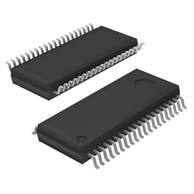
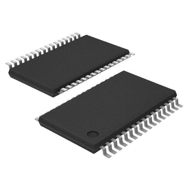
| 供应商器件封装 | 28-SO |
| 包装 | 带卷 (TR) |
| 商标 | STMicroelectronics |
| 增益 | 11.25 dB |
| 安装类型 | 表面贴装 |
| 安装风格 | SMD/SMT |
| 封装 | Reel |
| 封装/外壳 | 28-SOIC(0.295",7.50mm 宽) |
| 封装/箱体 | SO-28 |
| 工作电源电压 | 10 V |
| 工厂包装数量 | 1000 |
| 应用 | Hi-Fi 系统 |
| 最大工作温度 | + 85 C |
| 最小工作温度 | - 40 C |
| 标准包装 | 1,000 |
| 电源电压-最大 | 10 V |
| 电源电压-最小 | 6 V |
| 电源电流 | 8 mA |
| 类型 | 立体声音频 |
| 系列 | TDA7303 |


- 商务部:美国ITC正式对集成电路等产品启动337调查
- 曝三星4nm工艺存在良率问题 高通将骁龙8 Gen1或转产台积电
- 太阳诱电将投资9.5亿元在常州建新厂生产MLCC 预计2023年完工
- 英特尔发布欧洲新工厂建设计划 深化IDM 2.0 战略
- 台积电先进制程称霸业界 有大客户加持明年业绩稳了
- 达到5530亿美元!SIA预计今年全球半导体销售额将创下新高
- 英特尔拟将自动驾驶子公司Mobileye上市 估值或超500亿美元
- 三星加码芯片和SET,合并消费电子和移动部门,撤换高东真等 CEO
- 三星电子宣布重大人事变动 还合并消费电子和移动部门
- 海关总署:前11个月进口集成电路产品价值2.52万亿元 增长14.8%


PDF Datasheet 数据手册内容提取
TDA7303 Digital controlled stereo audio processor with loudness Features ■ Input multiplexer: – 3 stereo inputs – Selectable input gain for optimal adaptation to different sources ■ Volume control in 1.25 dB steps ■ Loudness function SO-28 ■ Treble and bass controL ■ Four speaker attenuators: – 4 independent speakers control in 1.25d B steps for balance and fader facilities Selectable input gain and external loudness – Independent mute function function are provided. Control is accomplished by ■ All functions programmable via serial I2C bus serial I2C bus microprocessor interface. The AC signal setting is obtained by resistor Description networks and switches combined with operational The TDA7303 is a volume, tone (bass and treble) amplifiers. balance (left/right) and fader (front/rear) Thanks to the used bipolar/CMOS technology, low processor for quality audio applications in car distortion, low noise and low DC stepping are radio, Hi-Fi and portable systems. obtained. T able 1. Device summary Order code Package Packing TDA7303 SO-28 Tray TDA7303TR SO-28 Tape and reel September 2013 Rev 4 1/20 1
Contents TDA7303 Contents 1 Block, test and pin diagrams . . . . . . . . . . . . . . . . . . . . . . . . . . . . . . . . . . 5 1.1 Block diagram . . . . . . . . . . . . . . . . . . . . . . . . . . . . . . . . . . . . . . . . . . . . . . . 5 1.2 Test circuit . . . . . . . . . . . . . . . . . . . . . . . . . . . . . . . . . . . . . . . . . . . . . . . . . 6 1.3 Pin connection . . . . . . . . . . . . . . . . . . . . . . . . . . . . . . . . . . . . . . . . . . . . . . 6 2 Electrical specifications . . . . . . . . . . . . . . . . . . . . . . . . . . . . . . . . . . . . . . 7 2.1 Absolute maximum ratings . . . . . . . . . . . . . . . . . . . . . . . . . . . . . . . . . . . . . 7 2.2 Quick reference data . . . . . . . . . . . . . . . . . . . . . . . . . . . . . . . . . . . . . . . . . 7 2.3 Thermal data . . . . . . . . . . . . . . . . . . . . . . . . . . . . . . . . . . . . . . . . . . . . . . . 7 2.4 Electrical characteristics . . . . . . . . . . . . . . . . . . . . . . . . . . . . . . . . . . . . . . . 8 2.5 Electrical characteristics curves . . . . . . . . . . . . . . . . . . . . . . . . . . . . . . . . 10 3 I2C bus interface . . . . . . . . . . . . . . . . . . . . . . . . . . . . . . . . . . . . . . . . . . . 13 3.1 Data validity . . . . . . . . . . . . . . . . . . . . . . . . . . . . . . . . . . . . . . . . . . . . . . . 13 3.2 Start and stop conditions . . . . . . . . . . . . . . . . . . . . . . . . . . . . . . . . . . . . . 13 3.3 Byte format . . . . . . . . . . . . . . . . . . . . . . . . . . . . . . . . . . . . . . . . . . . . . . . . 13 3.4 Acknowledge . . . . . . . . . . . . . . . . . . . . . . . . . . . . . . . . . . . . . . . . . . . . . . 13 3.5 Transmission without acknowledge . . . . . . . . . . . . . . . . . . . . . . . . . . . . . 13 4 Software specification . . . . . . . . . . . . . . . . . . . . . . . . . . . . . . . . . . . . . . 15 4.1 Interface protocol . . . . . . . . . . . . . . . . . . . . . . . . . . . . . . . . . . . . . . . . . . . 15 4.2 Subaddress (receive mode) . . . . . . . . . . . . . . . . . . . . . . . . . . . . . . . . . . . 15 4.3 Data bytes (detailed description) . . . . . . . . . . . . . . . . . . . . . . . . . . . . . . . 16 5 Package information . . . . . . . . . . . . . . . . . . . . . . . . . . . . . . . . . . . . . . . . 18 6 Revision history . . . . . . . . . . . . . . . . . . . . . . . . . . . . . . . . . . . . . . . . . . . 19 2/20
TDA7303 List of tables List of tables Table 1. Device summary. . . . . . . . . . . . . . . . . . . . . . . . . . . . . . . . . . . . . . . . . . . . . . . . . . . . . . . . . . 1 Table 2. Absolute maximum ratings. . . . . . . . . . . . . . . . . . . . . . . . . . . . . . . . . . . . . . . . . . . . . . . . . . 7 Table 3. Quick reference data . . . . . . . . . . . . . . . . . . . . . . . . . . . . . . . . . . . . . . . . . . . . . . . . . . . . . . 7 Table 4. Thermal data. . . . . . . . . . . . . . . . . . . . . . . . . . . . . . . . . . . . . . . . . . . . . . . . . . . . . . . . . . . . . 7 Table 5. Electrical characteristics. . . . . . . . . . . . . . . . . . . . . . . . . . . . . . . . . . . . . . . . . . . . . . . . . . . . 8 Table 6. Chip address. . . . . . . . . . . . . . . . . . . . . . . . . . . . . . . . . . . . . . . . . . . . . . . . . . . . . . . . . . . . 15 Table 7. Data bytes. . . . . . . . . . . . . . . . . . . . . . . . . . . . . . . . . . . . . . . . . . . . . . . . . . . . . . . . . . . . . . 15 Table 8. Volume . . . . . . . . . . . . . . . . . . . . . . . . . . . . . . . . . . . . . . . . . . . . . . . . . . . . . . . . . . . . . . . . 16 Table 9. Speaker attenuators. . . . . . . . . . . . . . . . . . . . . . . . . . . . . . . . . . . . . . . . . . . . . . . . . . . . . . 16 Table 10. Audio switch . . . . . . . . . . . . . . . . . . . . . . . . . . . . . . . . . . . . . . . . . . . . . . . . . . . . . . . . . . . . 17 Table 11. Bass and treble. . . . . . . . . . . . . . . . . . . . . . . . . . . . . . . . . . . . . . . . . . . . . . . . . . . . . . . . . . 17 Table 12. Document revision history . . . . . . . . . . . . . . . . . . . . . . . . . . . . . . . . . . . . . . . . . . . . . . . . . 19 3/20
List of figures TDA7303 List of figures Figure 1. Block diagram. . . . . . . . . . . . . . . . . . . . . . . . . . . . . . . . . . . . . . . . . . . . . . . . . . . . . . . . . . . . 5 Figure 2. Test circuit . . . . . . . . . . . . . . . . . . . . . . . . . . . . . . . . . . . . . . . . . . . . . . . . . . . . . . . . . . . . . . 6 Figure 3. Pin connection (top view) . . . . . . . . . . . . . . . . . . . . . . . . . . . . . . . . . . . . . . . . . . . . . . . . . . . 6 Figure 4. Loudness vs. volume attenuation. . . . . . . . . . . . . . . . . . . . . . . . . . . . . . . . . . . . . . . . . . . . 10 Figure 5. Loudness vs. frequency (CLOUD = 100 nF) vs. volume attenuation . . . . . . . . . . . . . . . . . 10 Figure 6. Loudness vs. external capacitors. . . . . . . . . . . . . . . . . . . . . . . . . . . . . . . . . . . . . . . . . . . . 10 Figure 7. Noise vs. volume/gain setting. . . . . . . . . . . . . . . . . . . . . . . . . . . . . . . . . . . . . . . . . . . . . . . 10 Figure 8. Signal to noise ratio vs. volume setting . . . . . . . . . . . . . . . . . . . . . . . . . . . . . . . . . . . . . . . 10 Figure 9. Distortion and noise vs. frequency (V = 1 V) . . . . . . . . . . . . . . . . . . . . . . . . . . . . . . . . . . 10 IN Figure 10. Distortion and noise vs. frequency (V = 250 mV). . . . . . . . . . . . . . . . . . . . . . . . . . . . . . . 11 IN Figure 11. Distortion vs. load resistance . . . . . . . . . . . . . . . . . . . . . . . . . . . . . . . . . . . . . . . . . . . . . . . 11 Figure 12. Channel separation (L Æ R) vs. frequency. . . . . . . . . . . . . . . . . . . . . . . . . . . . . . . . . . . . . 11 Figure 13. Input separation (L1 Æ L2, L3) vs. frequency. . . . . . . . . . . . . . . . . . . . . . . . . . . . . . . . . . . 11 Figure 14. Supply voltage rejection vs. frequency. . . . . . . . . . . . . . . . . . . . . . . . . . . . . . . . . . . . . . . . 11 Figure 15. Output clipping level vs. supply voltage . . . . . . . . . . . . . . . . . . . . . . . . . . . . . . . . . . . . . . . 11 Figure 16. Quiescent current vs. supply voltage . . . . . . . . . . . . . . . . . . . . . . . . . . . . . . . . . . . . . . . . . 12 Figure 17. Supply current vs. temperature. . . . . . . . . . . . . . . . . . . . . . . . . . . . . . . . . . . . . . . . . . . . . . 12 Figure 18. Bass resistance vs. temperature . . . . . . . . . . . . . . . . . . . . . . . . . . . . . . . . . . . . . . . . . . . . 12 Figure 19. Typical tone response (with the external components indicated in the test circuit) . . . . . . 12 Figure 20. Data validity on the I2C bus . . . . . . . . . . . . . . . . . . . . . . . . . . . . . . . . . . . . . . . . . . . . . . . . 14 Figure 21. Timing diagram of S-bus and I2C bus. . . . . . . . . . . . . . . . . . . . . . . . . . . . . . . . . . . . . . . . . 14 Figure 22. Acknowledge on the I2C bus . . . . . . . . . . . . . . . . . . . . . . . . . . . . . . . . . . . . . . . . . . . . . . . 14 Figure 23. Interface protocol . . . . . . . . . . . . . . . . . . . . . . . . . . . . . . . . . . . . . . . . . . . . . . . . . . . . . . . . 15 Figure 24. SO-28 mechanical data and package dimensions. . . . . . . . . . . . . . . . . . . . . . . . . . . . . . . 18 4/20
TDA7303 Block, test and pin diagrams 1 Block, test and pin diagrams 1.1 Block diagram Figure 1. Block diagram S U B OUT LEFTFRONT OUT LEFTREAR SCL SDA DIGGND OUT RIGHTFRONT OUT RIGHTREAR 5 3 8 7 6 4 2 2 2 2 2 2 2 2 8 SPKRATT TE SPKRATT MUTE SPKRATT MUTE SPKRATT TE D98AU88 U U M M L) R) C172.7nF TREBLE( EBLE + LATCHES EBLE TREBLE( 2.7nFC16 4 TR ER TR 5 00nFC15N(L) COD N(R) 00nFC13 1 BI DE BI 1 5.6KR2 BOUT(L) 18 RB BASS SERIAL BUS BASS RB 20 BOUT(R) 5.6KR1 C11100nF100nFC14OUD(L) 19 D D 21 OUD(R) 100nFC12 100nFC10 L LU LU L OO OO VL VL IN(L) 12 + + 8 IN(R) F F μ μ 2 6 6 2 2. 1 2. 9 8 C C UT(L) 17 R 7 UT(R) μ2F O INPUTSELECTO+ GAIN 1 OCREF 2C7 Y L 3 P L1 L2 L3 R3 R2 R1 SUP GND A 2 S V 5 4 3 0 1 1 1 1 9 1 1 1 2 3 3 2 1 FL L L R R R F 3xμ2 3xμ2 2.1 2 3 4 5 6 2. C C C C C C LEFTNPUTS RIGHTNPUTS I I 5/20
Block, test and pin diagrams TDA7303 1.2 Test circuit Figure 2. Test circuit 1.3 Pin connection Figure 3. Pin connection (top view) 6/20
TDA7303 Electrical specifications 2 Electrical specifications 2.1 Absolute maximum ratings T able 2. Absolute maximum ratings Symbol Parameter Value Unit V Operating supply voltage 10.0 V S T Ambient temperature -40 to 85 °C amb T Storage temperature range -55 to +150 °C stg 2.2 Quick reference data T able 3. Quick reference data Symbol Parameter Min. Typ. Max. Unit V Supply voltage 6 9 10 V S V Max. input signal handling 2 Vrms CL THD Total harmonic distortion V = 1 Vrms; f = 1 kHz 0.01 % S/N Signal to noise ratio 106 dB S Channel separation f = 1 kHz 103 dB C Volume control 1.25d B step -78.75 0 dB Bass and treble control 2 dB step -14 +14 dB Fader and balance control 1.25 dB step -38.75 0 dB Input gain 3.75 dB step1.25 dB step 0 11.25 dB Mute attenuation 100 dB 2.3 Thermal data T able 4. Thermal data Symbol Parameter Value Unit R Thermal resistance junction to pins Max. 85 °C/W th j-pins 7/20
Electrical specifications TDA7303 2.4 Electrical characteristics Table 5. E lectrical characteristics (T = 25 °C, V = 9 V, R = 10 k, R = 600 , all control flat (G = 0), f = 1 kHz unless amb S L G otherwise specified) Symbol Parameter Test condition Min. Typ. Max. Unit Supply V Supply voltage 6 9 10 V S I Supply current 8 11 mA S SVR Ripple rejection 60 80 dB Input selectors R Input resistance Input 1, 2, 3, 4 50 k II V Clipping level 2 2.5 Vrms CL S Input separation (2) 80 100 dB IN R Output load resistance pin 7, 17 2 k L G Min. input gain -1 0 1 dB INmin G Max. input gain 11.25 dB INmax G Step resolution 3.75 dB STEP e Input noise G = 11.25 dB 2 µV IN Volume control R Input resistance 33 k IN C Control range 70 75 80 dB RANGE A Min. attenuation -1 0 1 dB VMIN A Max. attenuation 70 75 80 dB VMAX A Step resolution 0.5 1.25 1.75 dB STEP A = 0 to -20 dB -1.25 0 1.25 dB V E Attenuation set error A A = -20 to -60 dB -3 2 dB V E Tracking error 2 dB T Speaker attenuators C Control range 35 37.5 40 dB range S Step resolution 0.5 1.25 1.75 dB STEP E Attenuation set error 1.5 dB A A Output mute attenuation 80 100 dB MUTE Bass control(1) Gb Control range Max. Boost/cut ±12 ±14 ±16 dB B Step resolution 1 2 3 dB STEP 8/20
TDA7303 Electrical specifications Table 5. Electrical characteristics (continued) (T = 25 °C, V = 9 V, R = 10 k, R = 600 , all control flat (G = 0), f = 1 kHz unless amb S L G otherwise specified) Symbol Parameter Test condition Min. Typ. Max. Unit R Internal feedback resistance 44 k B Treble control (1) Gt Control range Max. Boost/cut ±13 ±14 ±15 dB T Step Resolution 1 2 3 dB STEP Audio outputs V Clipping level d = 0.3 % 2 2.5 Vrms OCL R Output load resistance 2 k L C Output load capacitance 10 nF L R Output resistance 75 OUT V DC voltage level 4.2 4.5 4.8 V OUT General BW = 20-20 kHz, flat output muted 2.5 µV e Output noise(2) NO all gains = 0 dB 5 µV A curve all gains = 0 dB 3 µV S/N Signal to noise ratio all gains = 0 dB; V = 1 Vrms 106 dB O A = 0; V = 1 Vrms 0.01 % V IN d Distortion A = -20 dB, V = 1 Vrms 0.09 0.3 % V IN A = -20 dB, V = 0.3 Vrms 0.04 % V IN Sc Channel separation left/right 80 103 dB A = 0 to -20 dB 0 1 dB V Total tracking error -20 to -60 dB 0 2 dB Bus inputs V Input low voltage 1 V IL V Input high voltage 3 V IH I Input current -5 +5 µA IN V Output voltage SDA acknowledge I = 1.6 mA 0.4 V O O 1. Bass and treble response see attached diagram (Figure19). The center frequency and quality of the resonance behavior can be chosen by the external circuitry. A standard first order bass response can be realized by a standard feedback network 2. The selected input is grounded through the 2.2 µF capacitor. 9/20
Electrical specifications TDA7303 2.5 Electrical characteristics curves Figure 4. Loudness vs. volume attenuation Figure 5. Loudness vs. frequency (C = LOUD 100 nF) vs. volume attenuation Figure 6. Loudness vs. external capacitors Figure 7. Noise vs. volume/gain setting Figure 8. Signal to noise ratio vs. volume Figure 9. Distortion and noise vs. frequency setting (V = 1 V) IN 10/20
TDA7303 Electrical specifications Figure 10. Distortion and noise vs. frequency Figure 11. Distortion vs. load resistance (V = 250 mV) IN Figure 12. Channel separation (L R) vs. Figure 13. Input separation (L1 L2, L3) vs. frequency frequency Figure 14. Supply voltage rejection vs. Figure 15. Output clipping level vs. supply frequency voltage 11/20
Electrical specifications TDA7303 Figure 16. Quiescent current vs. supply Figure 17. Supply current vs. temperature voltage Figure 18. Bass resistance vs. temperature Figure 19. Typical tone response (with the external components indicated in the test circuit) 12/20
TDA7303 I2C bus interface 2 3 I C bus interface Data transmission from microprocessor to the TDA7303 and viceversa takes place through the 2 wires I2C bus interface, consisting of the two lines SDA and SCL (pull-up resistors to positive supply voltage must be connected). 3.1 Data validity As shown in Figure20, the data on the SDA line must be stable during the high period of the clock. The high and low state of the data line can only change when the clock signal on the SCL line is lOW. 3.2 Start and stop conditions As shown in Figure21 a start condition is a high to low transition of the SDA line while SCL is high. The stop condition is a low to high transition of the SDA line while SCL is high. 3.3 Byte format Every byte transferred on the SDA line must contain 8 bits. Each byte must be followed by an acknowledge bit. The MSB is transferred first. 3.4 Acknowledge The master (P) puts a resistive HIGH level on the SDA line during the acknowledge clock pulse (see Figure22). The peripheral (audioprocessor) that acknowledges has to pull-down (low) the SDA line during the acknowledge clock pulse, so that the SDA line is stable low during this clock pulse. The audioprocessor which has been addressed has to generate an acknowledge after the reception of each byte, otherwise the SDA line remains at the high level during the ninth clock pulse time. In this case the master transmitter can generate the stop information in order to abort the transfer. 3.5 Transmission without acknowledge Avoiding to detect the acknowledge of the audioprocessor, the P can use a simpler transmission: simply it waits one clock without checking the slave acknowledging, and sends the new data. This approach of course is less protected from misreading and decreases the noise immunity. 13/20
I2C bus interface TDA7303 Figure 20. Data validity on the I2C bus SDA SCL DATA LINE CHANGE STABLE, DATA DATA VALID ALLOWED D99AU1031 Figure 21. Timing diagram of S-bus and I2C bus SCL I2CBUS SDA START D99AU1032 STOP Figure 22. Acknowledge on the I2C bus SCL 1 2 3 7 8 9 SDA MSB ACKNOWLEDGMENT START D99AU1033 FROM RECEIVER Patent note: Purchase of I2C Components of STMicrolectronics, conveys a license under the Philips I2C Patent Rights to use these components in an I2C system, provided that the system conforms to the I2C Standard Specifications as defined by Philips. 14/20
TDA7303 Software specification 4 Software specification 4.1 Interface protocol The interface protocol comprises: ● A start condition (s) ● A chip address byte, containing the TDA7303 address (the 8th bit of the byte must be 0). The TDA7303 must always acknowledge at the end of each transmitted byte. ● A sequence of data (N-bytes + acknowledge) ● A stop condition (P) Figure 23. Interface protocol ACK = Acknowledge S = Start P = Stop Max. clock speed 400 kbits/s 4.2 Subaddress (receive mode) T able 6. Chip address MSB LSB 1 0 0 0 1 0 0 0 T able 7. Data bytes MSB LSB Function 0 0 B2 B1 B0 A2 A1 A0 Volume control 1 1 0 B1 B0 A2 A1 A0 Speaker ATT LR 1 1 1 B1 B0 A2 A1 A0 Speaker ATT RR 1 0 0 B1 B0 A2 A1 A0 Speaker ATT LF 1 0 1 B1 B0 A2 A1 A0 Speaker ATT RF 0 1 0 G1 G0 S2 S1 S0 Audio switch 0 1 1 0 C3 C2 C1 C0 Bass control 0 1 1 1 C3 C2 C1 C0 Treble control Ax = 1.25dB steps; Bx = 10dB steps; Cx = 2dB steps; Gx = 3.75dB steps 15/20
Software specification TDA7303 4.3 Data bytes (detailed description) T able 8. Volume MSB LSB Function 0 0 B2 B1 B0 A2 A1 A0 Volume 1.25 dB steps 0 0 0 0 0 0 1 -1.25 0 1 0 -2.5 0 1 1 -3.75 1 0 0 -5 1 0 1 -6.25 1 1 0 -7.5 1 1 1 -8.75 Volume 10 dB steps 0 0 0 0 0 0 1 -10 0 1 0 -20 0 1 1 -30 1 0 0 -40 1 0 1 -50 1 1 0 -60 1 1 1 -70 For example a volume of -45 dB is given by: 0 0 1 0 0 1 0 0 T able 9. Speaker attenuators MSB LSB Function 1 0 0 B1 B0 A2 A1 A0 Speaker LF 1 0 1 B1 B0 A2 A1 A0 Speaker RF 1 1 0 B1 B0 A2 A1 A0 Speaker LR 1 1 1 B1 B0 A2 A1 A0 Speaker RR 0 0 0 0 0 0 1 -1.25 0 1 0 -2.5 0 1 1 -3.75 1 0 0 -5 1 0 1 -6.25 1 1 0 -7.5 1 1 1 -8.75 0 0 0 0 1 -10 1 0 -20 1 1 -30 1 1 1 1 1 Mute For example attenuation of 25 dB on speaker RF is given by: 1 0 1 1 0 1 0 0 16/20
TDA7303 Software specification T able 10. Audio switch MSB LSB Function 0 1 0 G1 G0 S2 S1 S0 Audio Switch 0 0 Stereo 1 0 1 Stereo 2 1 0 Stereo 3 1 1 Not allowed 0 Loudness ON 1 Loudness OFF 0 0 +11.25 dB 0 1 +7.5 dB 1 0 +3.75d B 1 1 0 dB For example to select the stereo 2 input with a gain of +7.5dB LOUDNESS ON the 8bit string is: 0 1 0 0 1 0 0 1 T able 11. Bass and treble MSB LSB Function 0 1 1 0 C3 C2 C1 C0 Bass 0 1 1 1 C3 C2 C1 C0 Treble 0 0 0 0 -14 0 0 0 1 -12 0 0 1 0 -10 0 0 1 1 -8 0 1 0 0 -6 0 1 0 1 -4 0 1 1 0 -2 0 1 1 1 0 1 1 1 1 0 1 1 1 0 2 1 1 0 1 4 1 1 0 0 6 1 0 1 1 8 1 0 1 0 10 1 0 0 1 12 1 0 0 0 14 C3 = Sign For example Bass at -10dB is obtained by the following 8 bit string: 0 1 1 0 0 0 1 0 17/20
Package information TDA7303 5 Package information In order to meet environmental requirements, ST offers these devices in different grades of ECOPACK® packages, depending on their level of environmental compliance. ECOPACK® specifications, grade definitions and product status are available at: www.st.com. ECOPACK® is an ST trademark. Figure 24. SO-28 mechanical data and package dimensions mm inch DIM. OUTLINE AND MECHANICAL DATA MIN. TYP. MAX. MIN. TYP. MAX. A 2.65 0.104 a1 0.1 0.3 0.004 0.012 b 0.35 0.49 0.014 0.019 b1 0.23 0.32 0.009 0.013 C 0.5 0.020 c1 45° (typ.) D 17.7 18.1 0.697 0.713 E 10 10.65 0.394 0.419 e 1.27 0.050 e3 16.51 0.65 F 7.4 7.6 0.291 0.299 L 0.4 1.27 0.016 0.050 SO-28 S 8° (max.) 18/20
TDA7303 Revision history 6 Revision history T able 12. Document revision history Date Revision Changes 04-Aug-2006 1 Initial release. Updated “distortion” parameter in the Table5: Electrical characteristics on the page 9. 13-Mar-2009 2 Modified the max. clock speed value in Section4.1: Interface protocol on page15. Updated Section5: Package information on page18. Modified the test condition of the parameter “distortion” in the 18-Mar-2009 3 Table5: Electrical characteristics on the page 9. 17-Sep-2013 4 Updated Disclaimer 19/20
TDA7303 Please Read Carefully: Information in this document is provided solely in connection with ST products. STMicroelectronics NV and its subsidiaries (“ST”) reserve the right to make changes, corrections, modifications or improvements, to this document, and the products and services described herein at any time, without notice. All ST products are sold pursuant to ST’s terms and conditions of sale. Purchasers are solely responsible for the choice, selection and use of the ST products and services described herein, and ST assumes no liability whatsoever relating to the choice, selection or use of the ST products and services described herein. No license, express or implied, by estoppel or otherwise, to any intellectual property rights is granted under this document. If any part of this document refers to any third party products or services it shall not be deemed a license grant by ST for the use of such third party products or services, or any intellectual property contained therein or considered as a warranty covering the use in any manner whatsoever of such third party products or services or any intellectual property contained therein. UNLESS OTHERWISE SET FORTH IN ST’S TERMS AND CONDITIONS OF SALE ST DISCLAIMS ANY EXPRESS OR IMPLIED WARRANTY WITH RESPECT TO THE USE AND/OR SALE OF ST PRODUCTS INCLUDING WITHOUT LIMITATION IMPLIED WARRANTIES OF MERCHANTABILITY, FITNESS FOR A PARTICULAR PURPOSE (AND THEIR EQUIVALENTS UNDER THE LAWS OF ANY JURISDICTION), OR INFRINGEMENT OF ANY PATENT, COPYRIGHT OR OTHER INTELLECTUAL PROPERTY RIGHT. ST PRODUCTS ARE NOT DESIGNED OR AUTHORIZED FOR USE IN: (A) SAFETY CRITICAL APPLICATIONS SUCH AS LIFE SUPPORTING, ACTIVE IMPLANTED DEVICES OR SYSTEMS WITH PRODUCT FUNCTIONAL SAFETY REQUIREMENTS; (B) AERONAUTIC APPLICATIONS; (C) AUTOMOTIVE APPLICATIONS OR ENVIRONMENTS, AND/OR (D) AEROSPACE APPLICATIONS OR ENVIRONMENTS. WHERE ST PRODUCTS ARE NOT DESIGNED FOR SUCH USE, THE PURCHASER SHALL USE PRODUCTS AT PURCHASER’S SOLE RISK, EVEN IF ST HAS BEEN INFORMED IN WRITING OF SUCH USAGE, UNLESS A PRODUCT IS EXPRESSLY DESIGNATED BY ST AS BEING INTENDED FOR “AUTOMOTIVE, AUTOMOTIVE SAFETY OR MEDICAL” INDUSTRY DOMAINS ACCORDING TO ST PRODUCT DESIGN SPECIFICATIONS. PRODUCTS FORMALLY ESCC, QML OR JAN QUALIFIED ARE DEEMED SUITABLE FOR USE IN AEROSPACE BY THE CORRESPONDING GOVERNMENTAL AGENCY. Resale of ST products with provisions different from the statements and/or technical features set forth in this document shall immediately void any warranty granted by ST for the ST product or service described herein and shall not create or extend in any manner whatsoever, any liability of ST. ST and the ST logo are trademarks or registered trademarks of ST in various countries. Information in this document supersedes and replaces all information previously supplied. The ST logo is a registered trademark of STMicroelectronics. All other names are the property of their respective owners. © 2013 STMicroelectronics - All rights reserved STMicroelectronics group of companies Australia - Belgium - Brazil - Canada - China - Czech Republic - Finland - France - Germany - Hong Kong - India - Israel - Italy - Japan - Malaysia - Malta - Morocco - Philippines - Singapore - Spain - Sweden - Switzerland - United Kingdom - United States of America www.st.com 20/20
Mouser Electronics Authorized Distributor Click to View Pricing, Inventory, Delivery & Lifecycle Information: S TMicroelectronics: TDA7303TR