ICGOO在线商城 > 集成电路(IC) > 数据采集 - 模数转换器 > TC850CPL
 Datasheet下载
- 型号: TC850CPL
- 制造商: Microchip
- 库位|库存: xxxx|xxxx
- 要求:
| 数量阶梯 | 香港交货 | 国内含税 |
| +xxxx | $xxxx | ¥xxxx |
查看当月历史价格
查看今年历史价格
TC850CPL产品简介:
ICGOO电子元器件商城为您提供TC850CPL由Microchip设计生产,在icgoo商城现货销售,并且可以通过原厂、代理商等渠道进行代购。 TC850CPL价格参考。MicrochipTC850CPL封装/规格:数据采集 - 模数转换器, 15 Bit Analog to Digital Converter 1 Input 1 Dual Slope 40-PDIP。您可以下载TC850CPL参考资料、Datasheet数据手册功能说明书,资料中有TC850CPL 详细功能的应用电路图电压和使用方法及教程。
| 参数 | 数值 |
| 产品目录 | 集成电路 (IC)半导体 |
| 描述 | IC ADC 15BIT FAST 40DIP模数转换器 - ADC 16 Bit Hi Speed A/D |
| 产品分类 | |
| 品牌 | Microchip Technology |
| 产品手册 | |
| 产品图片 |
|
| rohs | 符合RoHS无铅 / 符合限制有害物质指令(RoHS)规范要求 |
| 产品系列 | 数据转换器IC,模数转换器 - ADC,Microchip Technology TC850CPL- |
| 数据手册 | http://www.microchip.com/mymicrochip/filehandler.aspx?ddocname=en011575 |
| 产品型号 | TC850CPL |
| PCN组件/产地 | http://www.microchip.com/mymicrochip/NotificationDetails.aspx?pcn=CYER-15WDGG555&print=viewhttp://www.microchip.com/mymicrochip/NotificationDetails.aspx?id=5509&print=viewhttp://www.microchip.com/mymicrochip/NotificationDetails.aspx?id=5777&print=view |
| 产品种类 | 模数转换器 - ADC |
| 位数 | 15 |
| 供应商器件封装 | 40-PDIP |
| 信噪比 | No |
| 分辨率 | 15 bit |
| 包装 | 管件 |
| 商标 | Microchip Technology |
| 安装类型 | 通孔 |
| 安装风格 | Through Hole |
| 封装 | Tube |
| 封装/外壳 | 40-DIP(0.600",15.24mm) |
| 封装/箱体 | PDIP-40 |
| 工作温度 | 0°C ~ 70°C |
| 工作电源电压 | +/- 5 V |
| 工厂包装数量 | 10 |
| 接口类型 | Parallel |
| 数据接口 | 并联 |
| 最大功率耗散 | 1230 mW |
| 最大工作温度 | + 70 C |
| 最小工作温度 | 0 C |
| 标准包装 | 10 |
| 电压参考 | External |
| 电压源 | 双 ± |
| 结构 | Multi-Slope |
| 转换器数 | 1 |
| 转换器数量 | 1 |
| 转换速率 | 40 S/s |
| 输入数和类型 | 1 个差分,单极 |
| 输入类型 | Differential |
| 通道数量 | 1 Channel |
| 采样率(每秒) | 40 |


- 商务部:美国ITC正式对集成电路等产品启动337调查
- 曝三星4nm工艺存在良率问题 高通将骁龙8 Gen1或转产台积电
- 太阳诱电将投资9.5亿元在常州建新厂生产MLCC 预计2023年完工
- 英特尔发布欧洲新工厂建设计划 深化IDM 2.0 战略
- 台积电先进制程称霸业界 有大客户加持明年业绩稳了
- 达到5530亿美元!SIA预计今年全球半导体销售额将创下新高
- 英特尔拟将自动驾驶子公司Mobileye上市 估值或超500亿美元
- 三星加码芯片和SET,合并消费电子和移动部门,撤换高东真等 CEO
- 三星电子宣布重大人事变动 还合并消费电子和移动部门
- 海关总署:前11个月进口集成电路产品价值2.52万亿元 增长14.8%


PDF Datasheet 数据手册内容提取
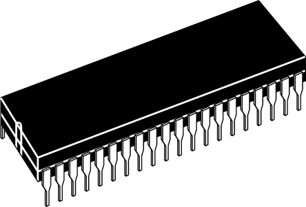
TC850 15-Bit, Fast Integrating CMOS A/D Converter Features Package Types • 15-bitResolutionPlusSignBit 40-Pin PDIP/CERDIP (cid:127) Upto40ConversionsperSecond CS 1 40 VDD (cid:127) IntegratingADCTechnique CE 2 39 REF1+ - Monotonic WR 3 38 CREF1+ - HighNoiseImmunity RD 4 37 CREF1- CONT/DEMAND 5 36 REF- - AutoZeroedAmplifiersEliminateOffset OVR/POL 6 35 CREF2- Trimming L/H 7 34 CREF2+ (cid:127) WideDynamicRange:96dB DB7 8 TC850CPL 33 REF2+ TC850IJL (cid:127) LowInputBiasCurrent:30pA DB6 9 32 IN+ DB5 10 31 IN- (cid:127) LowInputNoise:30 µVP-P DB4 11 30 ACNOAMLMOOGN (cid:127) Sensitivity:100 µV DB3 12 29 CINTB (cid:127) FlexibleOperationalControl DB2 13 28 CINTA DB1 14 27 CBUFA (cid:127) ContinuousorOnDemandConversions DB0 15 26 CBUFB (cid:127) DataValidOutput BUSY 16 25 BUFFER OSC1 17 24 INTIN (cid:127) BusCompatible,3-StateDataOutputs OSC2 18 23 INTOUT - 8-BitDataBus TEST 19 22 VSS - SimpleµPInterface DGND 20 21 COMP - TwoChipEnables - ReadADCResultLikeMemory 44-Pin PLCC D (cid:127) ±5VPowerSupplyOperation:20m Ω N A M (cid:127)A4p0p-PliincaDtuiaol-nins-Lineor44-PinPLCCPackages CONT/DE RD WR CE CS NC VDD REF+1C+REF1 C-REF1 REF- 6 5 4 3 2 1 44 43 42 41 40 (cid:127) PrecisionAnalogSignalProcessor OVR/POL 7 39CREF2- (cid:127) PrecisionSensorInterface L/H 8 38CREF2+ (cid:127) HighAccuracyDCMeasurements DB7 9 37REF2+ DB610 36IN+ Device Selection Table DB511 TC850CLW 35IN- NC12 TC850ILW 34NC Temperature DB413 33ANALOG PartNumber Package COMMON Range DB314 32CINTB TC850CPL 40-PinPDIP 0°Cto+70°C DB215 31CINTA TC850IJL 40-PinCERDIP -25°Cto+85°C DB116 30CBUFA TC850CLW 44-PinPLCC 0°Cto+70°C DB017 29CBUFB 18 19 20 21 22 23 24 25 26 27 28 TC850ILW 44-PinPLCC -25°Cto+85°C Y 1 2 T D C P S T N R BUS OSC OSC TES DGN N COM VSINTOU INTI BUFFE NC = No Internal Connection 2002MicrochipTechnologyInc. DS21479B-page 1
TC850 GeneralDescription need for precision external amplifiers. The internal amplifiersareautozeroed,ensuringazerodigitalout- TheTC850isamonolithicCMOSA/Dconverter(ADC) put, with 0V analog input. Zero adjustment withresolutionof15-bitsplussign.Itcombinesachop- potentiometersorcalibrationsarenotrequired. per-stabilizedbufferandintegratorwithauniquemulti- TheTC850outputsdataonan8-bit,3-statebus.Digital ple-slope integration technique that increases inputs are CMOS compatible while outputs are TTL/ conversionspeed.Theresultis16timesimprovement CMOScompatible.Chip-enableandbyte-selectinputs, in speed over previous 15-bit, monolithic integrating combined with an end-of-conversion output, ensures ADCs (from 2.5 conversions per second up to 40 per easy interfacing to a wide variety of microprocessors. second). Faster conversion speed is especially wel- Conversions can be performed continuously or on comeinsystemswithhumaninterface,suchasdigital command. In continuous mode, data is read as three scales. consecutivebytesandmanipulationofaddresslinesis TheTC850incorporatesanADCandaµP-compatible notrequired. digital interface. Only a voltage reference and a few, Operating from ±5V supplies, the TC850 dissipates noncritical,passivecomponentsarerequiredtoforma only20mΩ.TheTC850ispackagedina40-pinplastic complete15-bitplussignADC.CMOSprocessingpro- orceramicdual-in-linepackage(DIPs)andina44-pin vides the TC850 with high-impedance, differential plastic leaded chip carrier (PLCC), surface-mount inputs.Inputbiascurrentistypicallyonly30pA,permit- package. ting direct interface to sensors. Input sensitivity of 100µV per least significant bit (LSB) eliminates the FunctionalBlock Diagram Pinout of 40-Pin Package RINT CINT REF2+ –5V +5V REF1+ REF- BUF INT IN INT OUT 39 34 36 25 24 23 22 40 - 32 IN+ + - Comparator 31 Analog IN- Buffer + 30 Mux + COMMON Integrator - TC850 6-Bit 9-Bit A/D Up/Down Up/Down Control Counter Counter Sequencer Data Latch ÷4 Bus Interface Octal 2-Input Mux Clock Decode Logic Oscillator 3-State Data Bus 17 18 5 7 6 3 4 1 2 15 . . . .8 OSC1 OSC2 CONT/ L/HOVR/WR RD CS CE DB0 DB7 DEMAND POL DS21479B-page 2 2002MicrochipTechnologyInc.
TC850 1.0 ELECTRICAL SPECIFICATIONS *Stressesabovethoselistedunder"AbsoluteMaximumRat- ings"maycausepermanentdamagetothedevice.Theseare Absolute Maximum Ratings* stressratings only and functional operation of the device at these or any other conditions above those indicated in the PositiveSupplyVoltage..........................................+6V operationsectionsofthespecificationsisnotimplied.Expo- sure to Absolute Maximum Rating conditions for extended NegativeSupplyVoltage.......................................-9V periodsmayaffectdevicereliability. AnalogInputVoltage(IN+prIN-).............. V toV DD SS VoltageReferenceInput: (REF +,REF –,REF +)..................V toV 1 1 2 DD SS LogicInputVoltage.............V +0.3VtoGND–0.3V DD CurrentIntoAnyPin............................................10mA WhileOperating......................................100µA AmbientOperatingTemperatureRange CDevice.......................................0°Cto+70°C IDevice......................................-25°Cto+85°C PackagePowerDissipation(T ≤70°C) A CerDIP.....................................................2.29Ω PlasticDIP................................................1.23Ω PlasticPLCC ...........................................1.23Ω TC850ELECTRICALSPECIFICATIONS ElectricalCharacteristics:V =±5V;F =61.44kHz,V =3.2768V,T =25°C,Figure1-1,unlessotherwisespecified. S CLK FS A Symbol Parameter Min Typ Max Unit TestConditions ZeroScaleError ±0.25 ±0.5 LSB V =0V IN EndPointLinearityError — ±1 ±2 LSB -V ≤V ≤+V FS IN FS DifferentialNonlinearity — ±0.1 ±0.5 LSB I InputLeakageCurrent — 30 75 pA V =0V,T =25°C IN IN A — 1.1 3 nA -25°≤T ≤+85°C A V CommonModeVoltageRange V +1.5 — V –1.5 V OverOperatingTemperatureRange CMR SS SS CMRR CommonModeRejectionRatio — 80 — dB V =0V,V =±1V IN CM FullScaleGainTemperature — 2 5 ppm/°C ExternalRef.Temperature Coefficient Coefficient=0ppm/°C 0°C≤T ≤+70°C A ZeroScaleError — 0.3 2 µV/°C V =0V IN TemperatureCoefficient 0°C≤T ≤+70°C A FullScaleMagnitude — 0.5 2 LSB V =±3.275V IN SymmetryError e InputNoise — 30 — µV NotExceeded95%ofTime N P-P I + PositiveSupplyCurrent — 2 3.5 mA S I – NegativeSupplyCurrent — 2 3.5 mA S V OutputHighVoltage 3.5 4.9 — V I =500µA OH O V OutputLowVoltage — 0.15 0.4 V I =1.6mA OL O I OutputLeakageCurrent — 0.1 1 µA Pins8-15,High-ImpedanceState OP V InputHighVoltage 3.5 2.3 — V Note3 IH V InputLowVoltage — 2.1 1 V Note3 IL I InputPull-UpCurrent — 4 — µA Pins2,3,4,6,7;V =0V PU IN I InputPull-DownCurrent — 14 — µA Pins1,5;V =5V PD IN I OscillatorOutputCurrent — 140 — µA Pin18,V =2.5V OSC OUT C InputCapacitance — 1 — pF Pins1-7,17 IN C OutputCapacitance — 15 — pF Pins8-15,High-ImpedanceState OUT Note 1: Demandmode,CONT/DEMAND=LOW.Figure8-5timingdiagram.C =100pF. L 2: Continuousmode,CONT/DEMAND=HIGH.Figure8-7timingdiagram. 3: DigitalinputshaveCMOSlogiclevelsandinternalpull-up/pull-downresistors.ForTTLcompatibility,externalpull-up resistorstoV arerecommended. DD 2002MicrochipTechnologyInc. DS21479B-page 3
TC850 TC850ELECTRICALSPECIFICATIONS (CONTINUED) ElectricalCharacteristics:V =±5V;F =61.44kHz,V =3.2768V,T =25°C,Figure1-1,unlessotherwisespecified. S CLK FS A Symbol Parameter Min Typ Max Unit TestConditions T Chip-EnableAccessTime — 230 450 nsec CSorCE,RD=LOW(Note1) CE T Read-EnableAccessTime — 190 450 nsec CS=HIGH,CE=LOW,(Note1) RE T DataHoldFromCSorCE — 250 450 nsec RD=LOW,(Note1) DHC T DataHoldFromRD — 210 450 nsec CS=HIGH,CE=LOW,(Note1) DHR T OVR/POLDataAccessTime — 140 300 nsec CS=HIGH,CE=LOW, OP RD=LOW,(Note1) T Low/HighByteAccessTime — 140 300 nsec CS=HIGH,CE=LOW, LH RD=LOW,(Note1) ClockSetupTime 100 — — nsec PositiveorNegativePulseWidth T RDMinimumPulseWidth 450 230 — nsec CS=HIGH,CE=LOW,(Note2) WRE T RDMinimumDelayTime 150 50 — nsec CS=HIGH,CE=LOW,(Note2) WRD T WRMinimumPulseWidth 75 25 — nsec CS=HIGH,CE=LOW,(Note1) WWD Note 1: Demandmode,CONT/DEMAND=LOW.Figure8-5timingdiagram.C =100pF. L 2: Continuousmode,CONT/DEMAND=HIGH.Figure8-7timingdiagram. 3: DigitalinputshaveCMOSlogiclevelsandinternalpull-up/pull-downresistors.ForTTLcompatibility,externalpull-up resistorstoV arerecommended. DD DS21479B-page 4 2002MicrochipTechnologyInc.
TC850 FIGURE1-1: STANDARDTESTCIRCUITCONFIGURATION +5V -5V 40 20 22 VDD DGND VSS 32 100MΩ IN+ 16 BUSY 0.01µF Input 8 31 DB7 IN- 9 30 DB6 ANALOG COMMON +1.6384V 10 DB5 REF1+ 39 11 33 DB4 REF2+ 12 36 +0.0256V DB3 REF- 13 DB2 1145 DB1 TC850 CREF1+ 3378 1µF* DB0 CREF1- 1 34 23 CCSE CCRREEFF22+- 35 120M1kµΩF * WR 25 4 BUFFER 5 RCDONT/DEMAND INTIN 24 0R.I1NµTF 67 OVR/POL INTOUT 23 L/H C 17 INT OSC1 61.44 kHz 19 ** TEST NC 18 OSC2 21 ** COMP CINTA CINTB CBUFA CBUFB 28 29 27 26 0.1 0.1 0.1 0.1 0.1 µF µF µF µF µF NOTES: Unless otherwise specified, all 0.1µF capacitors are film dielectric. Ceramic capacitors are not recommended. NC = No Connection *Polypropylene capacitors. ** 100pF Mica capacitors. 2002MicrochipTechnologyInc. DS21479B-page 5
TC850 2.0 PIN DESCRIPTIONS ThedescriptionsofthepinsarelistedinTable. TABLE2-1: PINFUNCTIONTABLE PinNumber PinNumber (40-Pin Symbol Description (44-PinPLCC) PDIP/CERDIP) 1 2 CS Chipselect,activeHIGH.LogicallyANDed,withCEtoenablereadandwrite inputs(Note1). 2 3 CE Chipenable,activeLOW(Note2). 3 4 WR Writeinput,activeLOW.Whenchipisselected(CS=HIGHandCE=LOW)and indemandmode(CONT/DEMAND=LOW),alogicLOWonWRstartsa conversion(Note1). 4 5 RD Readinput,activeLOW.WhenCS=HIGHandCE=LOW,alogicLOWonRD enablesthe3-statedataoutputs(Note2). 5 6 CONT/ Conversioncontrolinput.WhenCONT/DEMAND=LOW,conversionsareiniti- DEMAND atedbytheWRinput.WhenCONT/DEMAND=HIGH,conversionsare performedcontinuously(Note1). 6 7 OVR/POL Overrange/polaritydata-selectinput.Whenmakingconversionsinthedemand mode(CONT/DEMAND=LOW),OVR/POLcontrolsthedataoutputonDB7 whenthehigh-orderbyteisactive(Note2). 7 8 L/H Low/highbyte-selectinput.WhenCONT/DEMAND=LOW,thisinputcontrols whetherlow-byteorhigh-bytedataisenabledonDB0throughDB7(Note2). 8 9 DB7 Mostsignificantdatabitoutput.WhenreadingtheA/Dconversionresult,the polarity,overrangeandDB7dataareoutputonthispin. 9-15 10-17 DB6-DB0 DataoutputsDB6-DB0.3-state,buscompatible. 16 18 BUSY A/Dconversionstatusoutput.BUSYgoestoalogicHIGHatthebeginningofthe de-integratephase,thengoesLOWwhenconversioniscomplete.Thefalling edgeofBUSYcanbeusedtogenerateaµPinterrupt. 17 19 OSC Crystaloscillatorconnectionorexternaloscillatorinput. 1 18 20 OSC Crystaloscillatorconnection. 2 19 21 TEST Forfactorytestingpurposesonly.Donotmakeexternalconnectiontothispin. 20 22 DGND Digitalgroundconnection. 21 24 COMP Connectionforcomparatorautozerocapacitor.BypasstoV with0.1µF. SS 22 25 V Negativepowersupplyconnection,typically-5V. SS 23 26 INT Outputoftheintegratoramplifier.ConnecttoC . OUT INT 24 27 INT Inputtotheintegratoramplifier.ConnecttosummingnodeofR andC . IN INT INT 25 28 BUFFER Outputoftheinputbuffer.ConnecttoR . INT 26 29 C Connectionforbufferautozerocapacitor.BypasstoV with0.1µF. BUFB SS 27 30 C Connectiontobufferautozerocapacitor.BypasstoV with0.1µF. BUFA SS 28 31 C Connectionforintegratorautozerocapacitor.BypasstoV with0.1µF. INTA SS 29 32 C Connectionforintegratorautozerocapacitor.BypasstoV with0.1µF. INTB SS 30 33 ANALOG Analogcommon. COMMON 31 35 IN– Negativedifferentialanaloginput. 32 36 IN+ Positivedifferentialanaloginput. Note 1: Thispinincorporatesapull-downresistortoDGND. 2: Thispinincorporatesapull-upresistortoV . DD 3: Pins1,23and34(44-PLCC)packageareNC“NoInternalconnection. DS21479B-page 6 2002MicrochipTechnologyInc.
TC850 TABLE2-1: PINFUNCTIONTABLE (CONTINUED) PinNumber PinNumber (40-Pin Symbol Description (44-PinPLCC) PDIP/CERDIP) 33 37 REF + PositiveinputforreferencevoltageV .(V =V /64) 2 REF2 REF2 REF1 34 38 C + PositiveconnectionforV referencecapacitor. REF2 REF2 35 39 C – NegativeconnectionforV referencecapacitor. REF2 REF2 36 40 REF– Negativeinputforreferencevoltages. 37 41 C – NegativeconnectionforV referencecapacitor. REF1 REF1 38 42 C + PositiveconnectionforV referencecapacitor. REF1 REF1 39 43 REF + PositiveinputforV . 1 REF1 40 44 V Positivepowersupplyconnection,typically+5V. DD Note 1: Thispinincorporatesapull-downresistortoDGND. 2: Thispinincorporatesapull-upresistortoV . DD 3: Pins1,23and34(44-PLCC)packageareNC“NoInternalconnection. 2002MicrochipTechnologyInc. DS21479B-page 7
TC850 3.0 DETAILED DESCRIPTION EQUATION3-1: ∫ The TC850 is a multiple-slope, integrating A/D con- 1 TINT VREFTDEINT V (T)DT= verter (ADC). The multiple-slope conversion process, RINTCINT 0 IN RINTCINT combinedwithchopper-stabilizedamplifiers,resultsin where: asignificantincreaseinADCspeed,whilemaintaining veryhighresolutionandaccuracy. VREF =Referencevoltage T =Signalintegrationtime(fixed) INT 3.1 DualSlope Conversion Principles T =Referencevoltageintegrationtime DEINT The conventional dual slope converter measurement (variable). cycle(showninFigure3-1)hastwodistinctphases: 3.2 Multiple Slope Conversion 1. Inputsignalintegration Principles 2. Referencevoltageintegration(de-integration). One limitation of the dual slope measurement tech- FIGURE3-1: DUAL SLOPEADCCYCLE nique is conversion speed. In a typical dual slope Signal De-integrate method, the auto zero and integrate times are each one-half of the de-integrate time. For a 15-bit conver- Reference De-integrate sion,214+214+215(65,536)clockpulsesarerequired for auto zero, integrate and de-integrate phases, respectively. The large number of clock cycles effec- End of Conversion tively limits the conversion rate to about 2.5 conver- Auto sions per second, when a typical analog CMOS Integrator Zero Output 0V fabricationprocessisused. Time TheTC850usesamultipleslopeconversiontechnique The input signal being converted is integrated for a to increase conversion speed (Figure3-2). This tech- fixedtimeperiod, measuredbycountingclockpulses. nique makes use of a two-slope de-integration phase Anoppositepolarityconstantreferencevoltageisthen andpermits15-bitresolutionupto40conversionsper de-integrateduntiltheintegratoroutputvoltagereturns second. to zero. The reference integration time is directly During the TC850'sde-integration phase, the integra- proportionaltotheinputsignal. tioncapacitorisrapidlydischargedtoyieldaresolution Inasimpledualslopeconverter, completeconversion of9bits. Atthispoint,somechargewillremainonthe requirestheintegratoroutputto"ramp-up"and"ramp- capacitor. This remaining charge is then slowly de- down." Most dual slope convertersadd athird phase, integrated,producinganadditional6bitsofresolution. autozero.Duringautozero,offsetvoltagesoftheinput The result is 15 bits of resolution achieved with only buffer, integrator and comparator are nulled, thereby 29+26 (512 + 64, or 576) clock pulses for de- eliminatingtheneedforzerooffsetadjustments. integration.Acompleteconversioncycleoccupiesonly 1280clockpulses. Dualslopeconverteraccuracyisunrelatedtotheinte- grating resistor and capacitor values, as long as they Inordertogenerate"fast-slow"de-integrationphases, arestableduringameasurementcycle.Byconverting twovoltagereferencesarerequired.Theprimaryrefer- the unknownanalog input voltageintoan easilymea- ence(VREF1)issettoone-halfofthefullscalevoltage sured function of time, the dual slope converter (typically VREF1 = 1.6384V, and VFS = 3.2768V). The reduces the need for expensive, precision passive secondaryvoltagereference(VREF2)issettoVREF1/64 components. (typically25.6mV).Tomaintain15-bitlinearity,atoler- anceof0.5%forV isrecommended. Noiseimmunityisaninherentbenefitoftheintegrating REF2 conversion method. Noise spikes are integrated, or averaged, to zero during the integration period. Inte- grating ADCs are immune to the large conversion errors that plague successive approximation convertersinhigh-noiseenvironments. A simple mathematical equation relates the input sig- nal,referencevoltageandintegrationtime: DS21479B-page 8 2002MicrochipTechnologyInc.
TC850 FIGURE3-2: “FASTSLOW” 4.0 ANALOG SECTION REFERENCE DE- DESCRIPTION INTEGRATIONCYCLE The TC850 analog section consists of an input buffer "Fast" Reference De-integrate amplifier, integrator amplifier, comparator and analog (9-Bit Resolution) switches. A simplified block diagram is shown in Figure4-1. "Slow" Reference De-integrate Signal Integrate (6-Bit Resolution) 4.1 Conversion Timing End of Conversion Eachconversionconsistsofthreephases: Auto 1. ZeroIntegrator Integrator Zero Output 0V 2. SignalIntegrate Time 3. ReferenceIntegrate(orDe-integrate) Each conversion cycle requires 1280 internal clock cycles(Figure4-2). FIGURE4-1: ANALOGSECTIONSIMPLIFIEDSCHEMATIC CREF1 CREF2 RINT CINT REF1+ REF1- CREF2- REF2+ CREF2- BUFF INTIN INTOUT CREF1+ CREF1- DE DE DE DE - Integrator* To Digital + – – Section Buffer* + + IN+ DE1 DE1 DE1 DE1 INT (-) (+) (-) (+) Comparator* Z1 DE1 DE1 DE2 DE2 (+) (-) (+) (-) ANALOG TC850 COMMON INT INT IN- *Auto Zeroed Amplifiers FIGURE4-2: CONVERSIONTIMING 1280 Clock Cyles Internal . . . . . . . . . . . . . . . . . . . . . Clock 246 256 778 Conversion Zero Integrator Signal Integrate Reference Integrate Phase 2002MicrochipTechnologyInc. DS21479B-page 9
TC850 4.2 Zero Integrator Phase 4.4 Reference Integrate Phase Duringthe zero integrator phase, thedifferential input Duringreferenceintegratephase,thechargestoredon signalisdisconnectedfromthecircuitbyopeninginter- the integrator capacitor is discharged. The time nal analog gates. The internal nodes are shorted to required to discharge the capacitor is proportional to analogcommon(ground)toestablishazeroinputcon- theanaloginputvoltage. dition. At the same time, a feedback loop is closed Thereferenceintegratephaseisdividedintothreesub- aroundtheinputbuffer,integratorandcomparator.The phases: feedbackloopensurestheintegratoroutputisnear0V 1. Fast beforethesignalintegratephasebegins. 2. Slow Duringthisphase,achopper-stabilizationtechniqueis usedtocanceloffseterrorsintheinputbuffer,integra- 3. Overrangede-integrate tor and comparator. Error voltages are stored on the Duringfastde-integrate,V -isinternallyconnectedto IN CBUFF,CINTandCOMPcapacitors.Thezerointegrate analogcommonandVIN+isconnectedacrossthepre- phaserequires246clockcycles. viously-chargedreferencecapacitor(C ).Theinte- REF1 gratorcapacitorisrapidlydischargedforamaximumof 4.3 SignalIntegrate Phase 512internalclockpulses,yielding9bitsofresolution. Thezerointegratorloopisopenedandtheinternaldif- During the slow de-integrate phase, the internal VIN+ ferentialinputsareconnectedtoIN+andIN-.Thediffer- nodeisnowconnectedtotheCREF2capacitorandthe ential inputsignalisintegratedfor afixedtimeperiod. residual charge on the integrator capacitor is further TheTC850signalintegrateperiodis256clockperiods, dischargedamaximumof64clockpulses.Atthispoint, orcounts.Thecrystaloscillatorfrequencyis÷4 before the analog input voltage has been converted with 15 clockingtheinternalcounters. bitsofresolution. Theintegrationtimeperiodis: Iftheanaloginputisgreaterthanfullscale,theTC850 performs up to three overrange de-integrate sub- EQUATION4-1: phases. Each subphase occupies a maximum of 64 clock pulses. The overrange feature permits analog 4x256 T = inputsupto192LSBsgreaterthanfullscaletobecor- INT F OSC rectlyconverted.This feature permitsthe user to digi- tallynullupto192countsofinputoffset,whileretaining full15-bitresolution. Inadditionto512countsoffast,64countsofslowand 192 counts of overrange de-integrate, the reference integratephaseuses10clockpulsestopermitinternal nodes to settle. Therefore, the reference integrate cycleoccupies778clockpulses. DS21479B-page 10 2002MicrochipTechnologyInc.
TC850 5.0 PIN DESCRIPTION (ANALOG) 5.1 DifferentialInputs (IN+ and IN–) TheanalogsignaltobemeasuredisappliedattheIN+ and IN– inputs. The differential input voltage must be withintheCommonmoderangeof theconverter. The inputCommonmoderangeextendsfromV -1.5Vto DD V +1.5V. Within this Common mode voltage range, SS an80dBCMRRistypical. The integrator output also follows the Common mode voltage. The integrator output must not be allowed to saturate. A worst-case condition exists, for example, when a large, positive Common mode voltage, with a near full scale negative differential input voltage, is applied.Thenegativeinputsignaldrivestheintegrator positive when most of its available swing has been used up by the positive Common mode voltage. For applicationswheremaximumCommonmoderangeis critical,integratorswingcanbereduced.Theintegrator output can swing within 0.4V of either supply without lossoflinearity. 5.2 DifferentialReference (V ) REF The TC850 requirestwo reference voltage sources in order togenerate the "fast-slow" de-integratephases. Themainvoltagereference(V )isappliedbetween REF1 the REF + and REF- pins. The secondary reference 1 (V )isappliedbetweentheREF +andREF-pins. REF2 2 The reference voltage inputs are fully differential and the reference voltage can be generated anywhere withinthepowersupplyvoltageoftheconverter.How- ever,tominimizerollovererror,especiallyathighcon- version rates, keep the reference Common mode voltage (i.e., REF-) near or at the analog common potential. All voltagereferenceinputsarehigh imped- ance. Averagereferenceinput currentistypicallyonly 30pA. 5.3 Analog Common (ANALOG COMMON) Analog common is used as the IN- return during the zero integrator and de-integrate phases of each con- version. If IN- is at a different potential than analog common, a Common mode voltage exists in the sys- tem.This signal isrejectedbythe80dBCMRR of the converter.However,inmostapplications,IN-willbeset at a fixed, known voltage (power supply common, for instance).Inthiscase,analogcommonshouldbetied tothesamepointsothattheCommonmodevoltageis eliminated. 2002MicrochipTechnologyInc. DS21479B-page11
TC850 6.0 DIGITAL SECTION (Figure1-1).Theoscillatoroutputis÷4prior toclock- DESCRIPTION ing the A/D internal counters. For example, a100kHz crystal produces a system clock frequency of 25kHz. TheTC850digitalsectionconsistsof twosetsofcon- Sinceeachconversionrequires1280clockperiods,in version counters, control and sequencing logic, clock this case the conversion rate will be 25,000/1280, or oscillatoranddivider,datalatchesandan8-bit,3-state 19.5conversionspersecond. interface bus. A simplified schematic of the bus inter- In most applications, however, an external clock is facelogicisshowninFigure6-1 divided down from the microprocessor clock. In this case, the OSC pin is used as the external oscillator 6.1 Clock Oscillator 1 inputandOSC isleftunconnected.Theexternalclock 2 TheTC850includesacrystaloscillatoron-chip.Allthat drivershouldswingfromdigitalgroundtoVDD.The÷4 is required is to connect a crystal across OSC and function is active for both external clock and crystal 1 OSC pins and to add two inexpensive capacitors oscillatoroperations. 2 FIGURE6-1: BUS INTERFACE SIMPLIFIEDSCHEMATIC 8 3-State Octal Low-Byte 8 Buffer 8 2-Input Mux 7 Up/Down DBO–DB7 Counter Output Enable Select L/H High-Byte Up/Down Counter RD CE To A/D Control Logic CS TC850 POL/OVR Select Polarity 2-Input Mux WR Start Overrange Conversion CONT/ DEMAND End of Conversion 6.2 Digital Operating Modes The low/high (L/H) byte-select and overrange/polarity (OVR/POL) inputs are disabled during continuous TwomodesofoperationareavailablewiththeTC850, modeoperation. Datamust bereadinthreeconsecu- continuous conversions and on-demand. The operat- tivebytes,asshowninTable6-1. ing mode is controlled by the CONT/DEMAND input. The bus interface method is different for continuous anddemandmodesofoperation. Note: Incontinuousmode,theconversionresultmust bereadwithin443-1/2clockcyclesoftheBUSY 6.2.1 DEMANDMODE OPERATION outputfallingedge.Afterthistime(i.e.,1/2clock cycle before BUSY goes high) the internal WhenCONT/DEMANDislow,theTC850performsone countersareresetandthedataislost. conversioneachtimethechipisselectedandtheWR inputispulsedlow.Dataisvalidonthefallingedgeof theBUSYoutputandcanbeaccessedusingtheinter- facetruthtable(Table6-1). 6.2.2 CONTINUOUS MODEOPERATION When CONT/DEMAND is high, the TC850 continu- ously performs conversions. Data will be valid on the falling edge of theBUSY output andremainsvalid for 443-1/2clockcycles. DS21479B-page 12 2002MicrochipTechnologyInc.
TC850 TABLE 6-1: BUS INTERFACETRUTHTABLE CE(cid:127)CS RD CONT/DEMAND L/H OVR/POL DB7 DB6–DB0 Pins1and2 Pin4 Pin5 Pin7 Pin6 Pin8 Pin9-Pin15(Note1) 0 0 0 0 0 "1"=InputPositive DataBits14-8 0 0 0 0 1 "1"=InputOverrange DataBits14-8 (Note2) 0 0 0 1 X DataBit7 DataBits6-0 0 0 1 X X Note3 0 1 X X X High-ImpedanceState 1 X X X X High-ImpedanceState Note 1: Pinnumbersreferto40-pinPDIP. 2: Extendedoverrangeoperation:Althoughratedat15bits(±32,767counts)ofresolution,theTC850providesanaddi- tional191countsabovefullscale.Forexample,withafull-scaleinputof3.2768V,themaximumanaloginputvoltage whichwillbeproperlyconvertedis3.2958V.Theextendedresolutionissignifiedbytheoverrangebitbeinghighandthe low-orderbytecontentsbeingbetween0and190.Forexample,withafull-scalevoltageof3.2768V: V OverrangeBit LowByte DataBits14–8 IN 3.2767V Low 255 127 10 10 3.2768V High 000 0 10 10 3.2769V High 001 0 10 10 3.2867V High 099 0 10 10 3: Continuousmodedatatransfer: a. Incontinuousmode,dataMUSTbereadinthreesequentialbytesaftertheBUSYoutputgoeslow: (1)Thefirstbytereadwillbethehigh-orderbyte,withDB7=polarity. (2)Thesecondbytereadwillcontainthelow-orderbyte. (3)Thethirdbytereadwillagainbethehigh-orderbyte,butwithDB7=overrange. b. Allthreedatabytesmustbereadwithin443-1/2clockcyclesafterthefallingedgeofBUSY. c. Thecinputmustgohighaftereachbyteisread,sothattheinternalbytecounterwillbeincremented. However,theCSandCEinputscanremainenabledthroughtheentiredatatransfersequence. 2002MicrochipTechnologyInc. DS21479B-page13
TC850 6.3 Pin Description (Digital) 6.3.6 CONTINUOUS/DEMANDMODE INPUT(CONT/DEMAND) 6.3.1 CHIPSELECTANDCHIPENABLE This input controls the TC850 operating mode. When (CS ANDCE) CONT/DEMANDisHIGH,theTC850performsconver- TheCSandCEinputspermiteasyinterfacingtoavari- sionscontinuously. Incontinuousmode, datamust be etyofdigitalbussystems.CEisactiveLOWwhileCS read in the prescribed sequence shown in Table6-1. is active HIGH. These inputs are logically ANDed Also, all three databytesmust bereadwithin443-1/2 internally and are used to enable the RD and WR internal clock cycles after the BUSY output goes low. inputs. After443-1/2clockcyclesdatawillbelost. When CONT/DEMAND is LOW, the TC850 begins a 6.3.2 WRITEENABLEINPUT(WR) conversioneachtimeCSandCEareactiveandWRis Thewriteinputisusedtoinitiateaconversionwhenthe being pulsed LOW. The conversion is complete and TC850isindemandmode.CSandCEmustbeactive datacanbereadafterthefallingedgeoftheBUSYout- for the WR input to be recognized. The status of the put. In demand mode, data can be read in any databusismeaninglessduringtheWRpulse,because sequence and remains valid until WR is again pulsed nodataisactuallywrittenintotheTC850. LOW. 6.3.3 READENABLEINPUT(RD) 6.3.7 BUSYOUTPUT(BUSY) Thereadinput,combinedwithCSandCE,enablethe TheBUSYoutputisusedtoconveyanend-of-conver- 3-statedatabusoutputs.Also,incontinuousmode,the sion to external logic. BUSY goes HIGH at thebegin- rising edge of the RD input activates an internal byte ning of the de-integrate phase and goes LOW at the countertosequentiallyreadthethreedatabytes. endoftheconversioncycle.Dataisvalidonthefalling edge of BUSY. The output-high period is fixed at 836 6.3.4 LOW/HIGHBYTE SELECT(L/H) clock periods, regardless of the analog input value. BUSY is active during continuous and demand mode TheL/Hinputdetermineswhetherthelow(leastsignif- operation. icant) byte or high (most significant) byte of data is placedonthe3-statedatabus.Thisinputismeaningful This output can also be used to generate an end-of- only when the TC850 is in the demand mode. In the conversion interrupt in µP-based systems. continuous mode, data must be read in three Noninterrupt-driven systems can poll BUSY to deter- predeterminedbytes,sotheL/Hinputisignored. minewhendataisvalid. 6.3.5 OVERRANGE/POLARITY BIT SELECT(OVR/POL) TheTC850provides15bitsofresolution,pluspolarity andoverrangebits.Thus,17bitsofinformationmustbe transferredonan8-bitdatabus.Toaccomplishthis,the overrangeandpolaritybitsaremultiplexedontodatabit DB7 of the most significant byte. When OVR/POL is HIGH,DB7ofthehighbytecontainstheoverrangesta- tus(HIGH=analoginputoverrange,LOW=inputwithin full scale). When OVR/POL is LOW, DB7 is HIGH for positive analog input polarity and LOW for negative polarity. The OVR/POL input is meaningful only when CS, CE and RD are active, and L/H is LOW (i.e., the mostsignificantbyteisselected).OVR/POLisignored whentheTC850isincontinuousmode. DS21479B-page 14 2002MicrochipTechnologyInc.
TC850 7.0 ANALOG SECTION TYPICAL 7.1.3 INTEGRATIONCAPACITOR APPLICATIONS The integration capacitor should be selected to pro- duce an integrator swing of ≈ 4V at full scale. The 7.1 Component Selection capacitorvalueiseasilycalculated: 7.1.1 REFERENCE VOLTAGE EQUATION7-4: The typical value for reference voltage VREF1 is VFS 4(cid:127)256 13..26736884VV.aTndhisresvoalluuteionyioefld1s00aµVfupllerssctaelpe.TvohletaVge of C= RINT (cid:127) 4VFCLOCK REF2 where: valueisderivedbydividingV by64.Thus,typical REF1 F isthecrystalorexternaloscillator CLOCK V value is 1.6384V/64, or 25.6mV. The V REF2 REF2 frequencyandV isthemaximuminputvoltage. FS valueshouldbeadjustedwithin±1%tomaintain15-bit accuracyforthetotalconversionprocess; The integration capacitor should be selected for low dielectric absorption to prevent rollover errors. A EQUATION7-1: : polypropylene, polyester or polycarbonate dielectric V ±1% capacitorisrecommended. V = REF1 REF 64 7.1.4 REFERENCE CAPACITORS Thereferencevoltageisnotlimitedtoexactly1.6384V, Thereferencecapacitorsrequirealow-leakagedielec- however, because the TC850 performs a ratiometric tric, such as polypropylene, polyester or polycarbon- conversion.Therefore,theconversionresultwillbe: ate.Avalueof1µFisrecommendedforoperationover thetemperaturerange.Ifhigh-temperatureoperationis EQUATION7-2: notrequired,theC valuescanbereduced. REF V DigitalCounts= IN (cid:127)16384 7.1.5 AUTOZEROCAPACITORS V REF1 Five capacitors are required to auto zero the input Thefullscalevoltagecanrangefrom3.2Vto3.5V.Full buffer, integrator amplifier and comparator. Recom- scalevoltagesoflessthan3.2Vwillresultinincreased mended capacitors are 0.1µF film dielectric (such as noise in the least significant bits, while a full scale polyester or polypropylene). Ceramic capacitors are above3.5Vwillexceedtheinputcommon-moderange. notrecommended. 7.1.2 INTEGRATIONRESISTOR TheTC850buffersupplies25µAofintegratorcharging currentwithminimallinearityerror.R iseasilycalcu- INT lated: EQUATION7-3: V FULLSCALE R = INT 25µA Forafullscalevoltageof3.2768V,valuesofR INT between120kΩand150kΩareacceptable. 2002MicrochipTechnologyInc. DS21479B-page15
TC850 8.0 DIGITAL SECTION TYPICAL FIGURE8-1: CRYSTALOSCILLATOR APPLICATIONS SCHEMATIC 10MΩ 8.1 Oscillator The TC850 may operate with a crystal oscillator. The ¸4 System crystalselectedshouldbedesignedforaPierceoscil- Clock lator,suchasanAT-cutquartzcrystal.Thecrystaloscil- TC850 latorschematicisshowninFigure8-1. 17 18 Since low frequency crystals are very large and 61.44kHz ceramic resonators are too lossy, the TC850 clock shouldbederived from anexternal source, suchasa 100pF 100pF microprocessorclock.Theclockshouldbeinputonthe OSC pin and no connection should be made to the 1 OSC pin. The external clock should swing between 2 DGNDandV . DD 8.2 Data Bus Interfacing Since oscillator frequency is ÷4 internally and each conversion requires 1280 internal clock cycles, the TheTC850providesaneasy andflexibledigital inter- conversiontimewillbe: face. A 3-state data bus and six control inputs permit theTC850tobetreatedasamemorydevice, inmost EQUATION8-1: applications. The conversion result can be accessed overan8-bitbusorviaaµPI/Oport. 4x1280 ConversionTime = A typical µP bus interface for the TC850 is shown in F CLOCK Figure8-2.Inthisexample,theTC850operatesinthe demand mode and conversion begins when a write An important advantage of the integrating ADC is the operationisperformedtoanydecodedaddressspace. abilitytorejectperiodicnoise.Thisfeatureismostoften TheBUSY output interrupts the µPat the end-of-con- used to reject line frequency (50Hz or 60Hz) noise. version. Noise rejection is accomplished by selecting the inte- gration period equal to one or more line frequency The A/D conversion result is read as three memory cycles. The desired clock frequency is selected as bytes.ThetwoLSBsoftheaddressbusselecthigh/low follows: byte and overrange/polarity bit data, while high-order addresslinesenabletheCEinput. EQUATION8-2: FIGURE8-2: INTERFACETOTYPICAL F =F x4x256 CLOCK NOISE µPDATABUS where: F isthenoisefrequencytoberejected, NOISE TC850 4representstheclockdivider, 256isthenumberofintegratecycles. DB0 DB0 DB1 DB1 DB2 DB2 For example, 60Hznoise will be rejected witha clock DB3 DB3 frequencyof 61.44kHz, givingaconversionrateof 12 DB4 DB4 conversions/sec. Integer submultiples of 61.44kHz DB5 DB5 µP DB6 DB6 (suchas30.72kHz,etc.)willalsoreject60Hznoise.For DB7 DB7 50Hz noise rejection, a 51.2kHz frequency is CE A2 Address recommended. Decode A. . . 15 Ifnoiserejectionisnotimportant,otherclockfrequen- L/H A0 cies can be used. The TC850 will typically operate at OVR/POL A1 conversionratesrangingfrom3to40conversions/sec, RD RD correspondingtooscillatorfrequenciesfrom15.36kHz WR WR BUSY INTERRUPT to204.8kHz. CS +5V CONT/DEMAND Address Data Bus X00 High Byte Polarity X01 Low Byte X10 High Byte Overrange DS21479B-page 16 2002MicrochipTechnologyInc.
TC850 Figure8-3showsatypicalinterfacetoaµPI/Oportor 8.3 Demand Mode Interface Timing single-chipµC.TheTC850operatesinthecontinuous mode and can either interrupt the µC/µP or be polled When CONT/DEMAND input is LOW, theTC850 per- withaninputpin. forms a conversion each time CE and CS are active andWRisstrobedLOW. FIGURE8-3: INTERFACETOTYPICAL The demand mode conversion timing is shown in µPI/OPORTORSINGLE- Figure8-4. BUSY goes LOW and data is valid 1155 CHIP µC clock pulses after WR goes LOW. After BUSY goes low,125additionalclockcyclesarerequiredbeforethe nextconversioncyclewillbegin. DB0 PA0 DB1 PA1 Once conversion is started, WR is ignored for 1100 DB2 PA2 internal clock cycles. After 1100 clock cycles, another DB3 PA3 WRpulseisrecognizedandinitiatesanewconversion DB4 PA4 DB5 PA5 µC OR µP when the present conversion is complete. A negative DB6 PA6 I/O PORT edgeonWR isrequiredto beginconversion.IfWRis DB7 PA7 heldLOW,conversionswillnotoccurcontinuously. TheA/Dconversiondataisvalidonthefallingedgeof BUSY INTERRUPT BUSY and remains valid until one-half internal clock RD PB0 cycle before BUSY goes HIGH on the succeeding conversion.BUSYcanbemonitoredwithanI/Opinto CONT/DEMAND +5V determineendofconversionortogenerateaµPinter- CS rupt. CE WR TC850 Indemand mode, the threedatabytescanbereadin any desired order. The TC850 is simply regarded as NC threebytesofmemoryandaccessedaccordingly.The busoutputtimingisshowninFigure8-5. SincethePA0-PA7inputsarededicatedtoreadingA/D data, the A/D CS/CE inputs can be enabled continu- 8.4 Continuous ModeInterfaceTiming ously. In continuous mode, data must be read in 3 When the CONT/DEMAND input is HIGH, the TC850 bytes,asshowninTable6-1. TherequiredRDpulses areprovidedbyaµC/µPoutputpin. performs conversions continuously. Data will be valid onthefallingedgeofBUSYandallthreebytesmustbe The circuit of Figure8-3 can also operate in the readwithin443-1/2internalclockcyclesofBUSYgoing demandmode,withthestart-upconversionstrobegen- LOW.ThetimingdiagramisshowninFigure8-6. eratedbyaµC/µPoutputpin.Inthiscase,theL/Hand In continuous mode, OVR/POL and L/H byte-select CONT/DEMAND inputs can be controlled by I/O pins inputs are ignored. The TC850 automatically cycles andtheRDinputconnectedtodigitalground. through three data bytes, as shown in Table6-1. Bus output timing in the continuous mode is shown in Figure8-7. 2002MicrochipTechnologyInc. DS21479B-page17
TC850 FIGURE8-4: CONVERSIONTIMING,DEMANDMODE . . . . . . . . . . . . Internal Clock CS . CE 1100 Clock Cycles WR Pulses are Ignored Next Convert Next Conversion WR Command will be can Begin Recognized 836 Clock Cycles 319 Clock 125 Clock Cycles Cycles BUSY DB0-DB7 Previous Conversion Data Meaningless New Conversion Data Valid Data Valid FIGURE8-5: BUS OUTPUTTIMING,DEMANDMODE TDHC TCE CS . CE TRE TDHR RD * DB0-DB6 HI-Z Data Bits 8 to 14 Data Bits 0 tp 6 High Impedance DB7 HI-Z "1"= Input "1"= Positive Data Bit 7 High Impedance Overrange Polarity tOP OVR/POL Don't Care TLH Don't Care L/H NOTE: CONT/DEMAND = LOW *RD (as well as CS and CE) can go HIGH after each byte is read (i.e., in a µP bus interface) or remain LOW during the entire DATA-READ sequence (i.e., µP I/O port interface). DS21479B-page 18 2002MicrochipTechnologyInc.
TC850 FIGURE8-6: CONVERSIONTIMING,CONTINUOUSMODE Internal . . . . . . . . . . . . . . . . . Clock 1280 Internal Clock Cycles Busy 836 Clock Cycles 443-1/2 Clock Cycles 1/2 Clock Cycle DB0-DB7 Data Meaningless Data Valid Data Meaningless FIGURE8-7: BUS OUTPUTTIMING,CONTINUOUSMODE CONT/DEMAND BUSY TWRE RD TRE TWRD DB0-DB7 HI-Z Data Bits 8-14 Data Bits 0-7 Data Bits 8-14 High Impedance Polarity Overrange State NOTES: CS = HIGH; CE = LOW 2002MicrochipTechnologyInc. DS21479B-page19
TC850 9.0 PACKAGING INFORMATION 9.1 Package Marking Information Packagemarkingdatanotavailableatthistime 9.2 Taping Form Component Taping Orientation for 44-Pin PLCC Devices User Direction of Feed PIN 1 W P Standard Reel Component Orientation for TR Suffix Device Carrier Tape, Number of Components Per Reel and Reel Size Package Carrier Width (W) Pitch (P) Part Per Full Reel Reel Size 44-Pin PLCC 32 mm 24 mm 500 13 in NOTE: Drawing does not represent total number of pins. 9.3 Package Dimensions 40-Pin CERDIP (Wide) PIN 1 .540 (13.72) .510 (12.95) .098 (2.49) MAX. .030 (0.76) MIN. 2.070 (52.58) .620 (15.75) 2.030 (51.56) .590 (15.00) .060 (1.52) .210 (5.33) .020 (0.51) .170 (4.32) .015 (0.38) .200 (5.08) .150 (3.81) .008 (0.20) 3˚ MIN. .125 (3.18) MIN. .700 (17.78) .620 (15.75) .110 (2.79) .065 (1.65) .020 (0.51) .090 (2.29) .045 (1.14) .016 (0.41) Dimensions: inches (mm) DS21479B-page 20 2002MicrochipTechnologyInc.
TC850 9.3 Package Dimensions (Continued) 40-Pin PDIP (Wide) PIN 1 .555 (14.10) .530 (13.46) 2.065 (52.45) .610 (15.49) 2.027 (51.49) .590 (14.99) .200 (5.08) .140 (3.56) .040 (1.02) ..115105 ((32..8912)) .020 (0.51) ..001058 ((00..3280)) 3˚ MIN. .700 (17.78) .610 (15.50) .110 (2.79) .070 (1.78) .022 (0.56) .090 (2.29) .045 (1.14) .015 (0.38) Dimensions: inches (mm) 44-Pin PLCC PIN 1 .050 (1.27) TYP. .021 (0.53) .013 (0.33) .695 (17.65) .685 (17.40) .630 (16.00) .591 (15.00) .656 (16.66) .650 (16.51) .032 (0.81) .026 (0.66) .020 (0.51) MIN. .656 (16.66) .650 (16.51) .120 (3.05) .695 (17.65) .090 (2.29) .685 (17.40) .180 (4.57) .165 (4.19) Dimensions: inches (mm) 2002MicrochipTechnologyInc. DS21479B-page21
TC850 NOTES: DS21479B-page 22 2002MicrochipTechnologyInc.
TC850 SALES AND SUPPORT DataSheets ProductssupportedbyapreliminaryDataSheetmayhaveanerratasheetdescribingminoroperationaldifferencesandrecom- mendedworkarounds.Todetermineifanerratasheetexistsforaparticulardevice,pleasecontactoneofthefollowing: 1. YourlocalMicrochipsalesoffice 2. TheMicrochipCorporateLiteratureCenterU.S.FAX:(480)792-7277 3. TheMicrochipWorldwideSite(www.microchip.com) Pleasespecifywhichdevice,revisionofsiliconandDataSheet(includeLiterature#)youareusing. NewCustomerNotificationSystem Registeronourwebsite(www.microchip.com/cn)toreceivethemostcurrentinformationonourproducts. S 2002MicrochipTechnologyInc. DS21479B-page23
TC850 NOTES: DS21479B-page 24 2002MicrochipTechnologyInc.
TC850 Information contained in this publication regarding device Trademarks applicationsandthelikeisintendedthroughsuggestiononly andmaybesupersededbyupdates.Itisyourresponsibilityto The Microchip name and logo, the Microchip logo, FilterLab, ensure that your application meets with your specifications. KEELOQ, microID, MPLAB, PIC, PICmicro, PICMASTER, No representation or warranty is given and no liability is PICSTART,PROMATE, SEEVAL and TheEmbedded Control assumedbyMicrochipTechnologyIncorporatedwithrespect SolutionsCompanyareregisteredtrademarksofMicrochipTech- totheaccuracyoruseofsuchinformation,orinfringementof nologyIncorporatedintheU.S.A.andothercountries. patentsorotherintellectualpropertyrightsarisingfromsuch dsPIC,ECONOMONITOR,FanSense,FlexROM,fuzzyLAB, useorotherwise.UseofMicrochip’sproductsascriticalcom- In-Circuit Serial Programming, ICSP, ICEPIC, microPort, ponentsinlifesupportsystemsisnotauthorizedexceptwith Migratable Memory, MPASM, MPLIB, MPLINK, MPSIM, expresswritten approvalbyMicrochip.Nolicensesarecon- MXDEV, PICC, PICDEM, PICDEM.net, rfPIC, Select Mode veyed,implicitlyorotherwise,underanyintellectualproperty andTotalEndurancearetrademarksofMicrochipTechnology rights. IncorporatedintheU.S.A. SerializedQuickTurnProgramming(SQTP)isaservicemark ofMicrochipTechnologyIncorporatedintheU.S.A. All other trademarks mentioned herein are property of their respectivecompanies. © 2002, Microchip Technology Incorporated, Printed in the U.S.A.,AllRightsReserved. Printedonrecycledpaper. MicrochipreceivedQS-9000qualitysystem certificationforitsworldwideheadquarters, designandwaferfabricationfacilitiesin ChandlerandTempe,ArizonainJuly1999 andMountainView,CaliforniainMarch2002. TheCompany’squalitysystemprocessesand proceduresareQS-9000compliantforits PICmicro®8-bitMCUs,KEELOQ®codehopping devices,SerialEEPROMs,microperipherals, non-volatilememoryandanalogproducts.In addition,Microchip’squalitysystemforthe designandmanufactureofdevelopment systemsisISO9001certified. 2002MicrochipTechnologyInc. DS21479B-page25
WORLDWIDE SALES AND SERVICE AMERICAS ASIA/PACIFIC Japan CorporateOffice Australia MicrochipTechnologyJapanK.K. BenexS-16F 2355WestChandlerBlvd. MicrochipTechnologyAustraliaPtyLtd 3-18-20,Shinyokohama Chandler,AZ 85224-6199 Suite22,41RawsonStreet Kohoku-Ku,Yokohama-shi Tel: 480-792-7200 Fax: 480-792-7277 Epping2121,NSW Kanagawa,222-0033,Japan TechnicalSupport:480-792-7627 Australia Tel:81-45-471-6166 Fax:81-45-471-6122 WebAddress:http://www.microchip.com Tel:61-2-9868-6733Fax:61-2-9868-6755 Korea RockyMountain China-Beijing 2355WestChandlerBlvd. Microchip Technology Consulting (Shanghai) MicrochipTechnologyKorea 168-1,YoungboBldg.3Floor Chandler,AZ 85224-6199 Co.,Ltd.,BeijingLiaisonOffice Samsung-Dong,Kangnam-Ku Tel: 480-792-7966 Fax: 480-792-7456 Unit915 BeiHaiWanTaiBldg. Seoul,Korea135-882 Atlanta Tel:82-2-554-7200 Fax:82-2-558-5934 No.6ChaoyangmenBeidajie 500SugarMillRoad,Suite200B Beijing,100027,No.China Singapore Atlanta,GA 30350 Tel:86-10-85282100Fax:86-10-85282104 MicrochipTechnologySingaporePteLtd. Tel:770-640-0034 Fax:770-640-0307 China-Chengdu 200MiddleRoad Boston #07-02PrimeCentre Microchip Technology Consulting (Shanghai) 2LanDrive,Suite120 Singapore,188980 Co.,Ltd.,ChengduLiaisonOffice Westford,MA 01886 Tel: 65-6334-8870 Fax:65-6334-8850 Rm.2401,24thFloor, Tel:978-692-3848 Fax:978-692-3821 MingXingFinancialTower Taiwan Chicago No.88TIDUStreet MicrochipTechnologyTaiwan 333PierceRoad,Suite180 Chengdu610016,China 11F-3,No.207 Itasca,IL 60143 Tel:86-28-86766200 Fax:86-28-86766599 TungHuaNorthRoad Tel:630-285-0071Fax:630-285-0075 Taipei,105,Taiwan China-Fuzhou Dallas Tel:886-2-2717-7175 Fax:886-2-2545-0139 Microchip Technology Consulting (Shanghai) 4570WestgroveDrive,Suite160 Co.,Ltd.,FuzhouLiaisonOffice Addison,TX75001 Unit28F,WorldTradePlaza EUROPE Tel:972-818-7423 Fax:972-818-2924 No.71WusiRoad Detroit Fuzhou350001,China Denmark Tri-AtriaOfficeBuilding Tel:86-591-7503506 Fax:86-591-7503521 MicrochipTechnologyNordicApS 32255NorthwesternHighway,Suite190 China-Shanghai RegusBusinessCentre FarmingtonHills,MI 48334 Microchip Technology Consulting (Shanghai) Lautruphoj1-3 Tel:248-538-2250Fax:248-538-2260 BallerupDK-2750Denmark Co.,Ltd. Kokomo Room701,Bldg.B Tel:4544209895Fax:4544209910 2767S.AlbrightRoad FarEastInternationalPlaza France Kokomo,Indiana 46902 No.317XianXiaRoad MicrochipTechnologySARL Tel:765-864-8360Fax:765-864-8387 Shanghai,200051 Parcd’ActiviteduMoulindeMassy LosAngeles Tel:86-21-6275-5700 Fax:86-21-6275-5060 43RueduSauleTrapu 18201VonKarman,Suite1090 China-Shenzhen BatimentA-lerEtage Irvine,CA 92612 Microchip Technology Consulting (Shanghai) 91300Massy,France Tel:949-263-1888 Fax:949-263-1338 Co.,Ltd.,ShenzhenLiaisonOffice Tel:33-1-69-53-63-20 Fax:33-1-69-30-90-79 NewYork Rm.1315,13/F,ShenzhenKerryCentre, Germany 150MotorParkway,Suite202 RenminnanLu MicrochipTechnologyGmbH Hauppauge,NY 11788 Shenzhen518001,China Gustav-HeinemannRing125 Tel:631-273-5305 Fax:631-273-5335 Tel:86-755-2350361 Fax:86-755-2366086 D-81739Munich,Germany SanJose China-HongKongSAR Tel:49-89-627-1440 Fax:49-89-627-144-44 Italy MicrochipTechnologyInc. MicrochipTechnologyHongkongLtd. 2107NorthFirstStreet,Suite590 Unit901-6,Tower2,Metroplaza MicrochipTechnologySRL SanJose,CA 95131 223HingFongRoad CentroDirezionaleColleoni Tel:408-436-7950 Fax:408-436-7955 KwaiFong,N.T.,HongKong PalazzoTaurus1V.LeColleoni1 Toronto Tel:852-2401-1200 Fax:852-2401-3431 20041AgrateBrianza Milan,Italy 6285NorthamDrive,Suite108 India Tel:39-039-65791-1 Fax:39-039-6899883 Mississauga,OntarioL4V1X5,Canada MicrochipTechnologyInc. UnitedKingdom Tel:905-673-0699 Fax: 905-673-6509 IndiaLiaisonOffice DivyasreeChambers MicrochipLtd. 505EskdaleRoad 1Floor,WingA(A3/A4) WinnershTriangle No.11,O’ShaugnesseyRoad Bangalore,560025,India Wokingham Berkshire,EnglandRG415TU Tel:91-80-2290061Fax:91-80-2290062 Tel:441189215869 Fax:44-118921-5820 04/20/02 *DS21479B* DS21479B-page 26 2002MicrochipTechnologyInc.
Mouser Electronics Authorized Distributor Click to View Pricing, Inventory, Delivery & Lifecycle Information: M icrochip: TC850ILW TC850CLW TC850CPL TC850CLW713