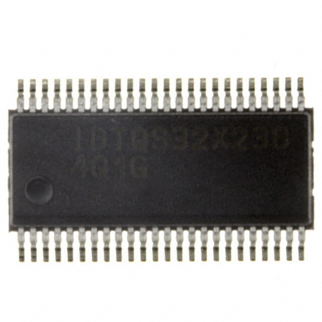
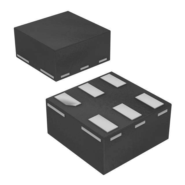
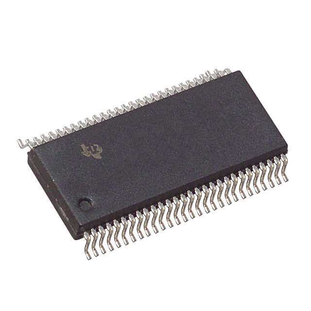
ICGOO在线商城 > 集成电路(IC) > 逻辑 - 信号开关,多路复用器,解码器 > TC7WB66CFK,LF
- 型号: TC7WB66CFK,LF
- 制造商: Toshiba America Electronic Components, Inc.
- 库位|库存: xxxx|xxxx
- 要求:
| 数量阶梯 | 香港交货 | 国内含税 |
| +xxxx | $xxxx | ¥xxxx |
查看当月历史价格
查看今年历史价格
TC7WB66CFK,LF产品简介:
ICGOO电子元器件商城为您提供TC7WB66CFK,LF由Toshiba America Electronic Components, Inc.设计生产,在icgoo商城现货销售,并且可以通过原厂、代理商等渠道进行代购。 TC7WB66CFK,LF价格参考。Toshiba America Electronic Components, Inc.TC7WB66CFK,LF封装/规格:逻辑 - 信号开关,多路复用器,解码器, Bus Switch 2 x 1:1 US8。您可以下载TC7WB66CFK,LF参考资料、Datasheet数据手册功能说明书,资料中有TC7WB66CFK,LF 详细功能的应用电路图电压和使用方法及教程。
| 参数 | 数值 |
| 产品目录 | 集成电路 (IC) |
| 描述 | IC DUAL BUS SWITCH US8 |
| 产品分类 | |
| 品牌 | Toshiba Semiconductor and Storage |
| 数据手册 | http://www.semicon.toshiba.co.jp/info/docget.jsp?pid=TC7WB66CFK&lang=en&type=datasheet |
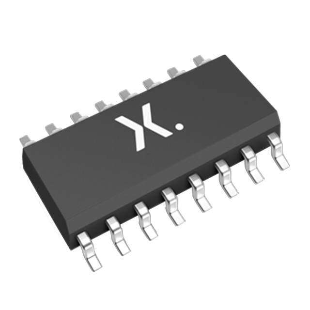
| 产品图片 |
|
| 产品型号 | TC7WB66CFK,LF |
| rohs | 无铅 / 符合限制有害物质指令(RoHS)规范要求 |
| 产品系列 | TC7WB |
| 供应商器件封装 | US8 |
| 其它名称 | TC7WB66CFKLFCT |
| 包装 | 剪切带 (CT) |
| 安装类型 | 表面贴装 |
| 封装/外壳 | 8-VFSOP(0.091",2.30mm 宽) |
| 工作温度 | -40°C ~ 85°C |
| 标准包装 | 1 |
| 独立电路 | 1 |
| 电压-电源 | 1.65 V ~ 5.5 V |
| 电压源 | 单电源 |
| 电流-输出高,低 | - |
| 电路 | 2 x 1:1 |
| 类型 | 总线开关 |
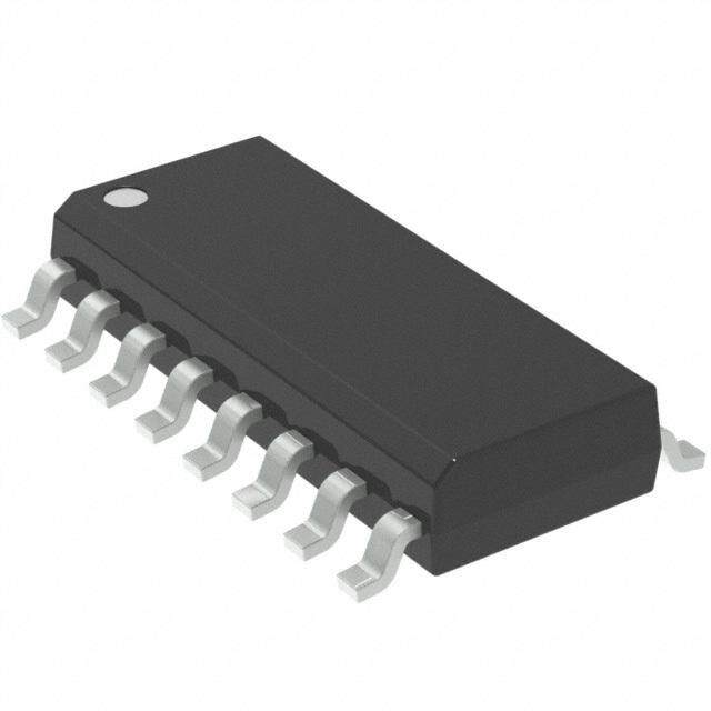



PDF Datasheet 数据手册内容提取
TC7WB66CFK/L8X,TC7WB67CFK/L8X CMOS Digital Integrated Circuits Silicon Monolithic TTTTCCCC7777WWWWBBBB66666666CCCCFFFFKKKK,,,,TTTTCCCC7777WWWWBBBB66666666CCCCLLLL8888XXXX TTTTCCCC7777WWWWBBBB66667777CCCCFFFFKKKK,,,,TTTTCCCC7777WWWWBBBB66667777CCCCLLLL8888XXXX 1111.... FFFFuuuunnnnccccttttiiiioooonnnnaaaallll DDDDeeeessssccccrrrriiiippppttttiiiioooonnnn • Dual SPST Bus Switch 2222.... GGGGeeeennnneeeerrrraaaallll The TC7WB66CFK/L8X and TC7WB67CFK/L8X are low ON-resistance, high-speed CMOS 2-bit bus switches. These bus switches allow connections or disconnections to be made with minimal propagation delay while maintaining Low power dissipation which is the feature of CMOS. TC7WB66CFK/L8X requires the output enable (OE) input to be set low to place the output into the high impedance state,whereas the TC7WB67CFK/L8X requires the output enable (OE) input to be set high to place the output into the high impedance. These Bus switches consist of P-MOS and N-MOS structure, meaning these devices are suitable for analog signal transmission. All inputs are equipped with protector circuits to protect the device from static discharge. 3333.... FFFFeeeeaaaattttuuuurrrreeeessss (1) Operating voltage: V = 1.65 to 5.5 V CC (2) ON capacitance: C = 10 pF Switch On (typ.) @V = 5.0 V I/O CC (3) ON resistance: RON = 4 Ω (typ.) @VCC = 4.5 V, VIS = 0 V (4) ESD performance: Machine model ≥ ±200 V, Human body model ≥ ±2000 V (5) Package: US8, MP8 4444.... PPPPaaaacccckkkkaaaaggggiiiinnnngggg TC7WB66CFK,TC7WB67CFK TC7WB66CL8X,TC7WB67CL8X US8 MP8 Start of commercial production 2012-10 ©2015-2018 1 2018-10-22 Toshiba Electronic Devices & Storage Corporation Rev.4.0
TC7WB66CFK/L8X,TC7WB67CFK/L8X 5555.... PPPPiiiinnnn AAAAssssssssiiiiggggnnnnmmmmeeeennnntttt TC7WB66CFK TC7WB67CFK TC7WB66CL8X TC7WB67CL8X 6666.... MMMMaaaarrrrkkkkiiiinnnngggg TC7WB66CFK TC7WB67CFK TC7WB66CL8X TC7WB67CL8X ©2015-2018 2 2018-10-22 Toshiba Electronic Devices & Storage Corporation Rev.4.0
TC7WB66CFK/L8X,TC7WB67CFK/L8X 7777.... BBBBlllloooocccckkkk DDDDiiiiaaaaggggrrrraaaammmm TC7WB66CFK,TC7WB66CL8X TC7WB67CFK,TC7WB67CL8X 8888.... PPPPrrrriiiinnnncccciiiipppplllleeee ooooffff OOOOppppeeeerrrraaaattttiiiioooonnnn 8888....1111.... TTTTrrrruuuutttthhhh TTTTaaaabbbblllleeee Inputs OE Inputs OE Function (TC7WB66CFK/L8X) (TC7WB67CFK/L8X) H L A port = B port L H Disconnect 9999.... AAAAbbbbssssoooolllluuuutttteeee MMMMaaaaxxxxiiiimmmmuuuummmm RRRRaaaattttiiiinnnnggggssss ((((NNNNooootttteeee)))) Characteristics Part Number Symbol Note Rating Unit Supply voltage V -0.5 to 7.0 V CC Input voltage (OE, OE) V -0.5 to 7.0 IN Switch I/O voltage V -0.5 to V +0.5 S CC Clamp diode current I -50 mA IK Switch I/O current I 50 S Power dissipation TC7WB66CFK,TC7WB67CFK P 200 mW D TC7WB66CL8X,TC7WB67CL8X (Note 1) 300 V /ground current I /I ±100 mA CC CC GND Storage temperature T -65 to 150 stg Note: Exceeding any of the absolute maximum ratings, even briefly, lead to deterioration in IC performance or even destruction. Using continuously under heavy loads (e.g. the application of high temperature/current/voltage and the significant change in temperature, etc.) may cause this product to decrease in the reliability significantly even if the operating conditions (i.e. operating temperature/current/voltage, etc.) are within the absolute maximum ratings and the operating ranges. Please design the appropriate reliability upon reviewing the Toshiba Semiconductor Reliability Handbook (“Handling Precautions”/“Derating Concept and Methods”) and individual reliability data (i.e. reliability test report and estimated failure rate, etc). Note 1:Mounted on an FR4 board 11110000.... OOOOppppeeeerrrraaaattttiiiinnnngggg RRRRaaaannnnggggeeeessss ((((NNNNooootttteeee)))) Characteristics Symbol Note Rating Unit Supply voltage V 1.65 to 5.5 V CC Input voltage (OE, OE) V 0 to 5.5 IN Switch I/O voltage V 0 to V S CC Operating temperature T -40 to 85 opr Input rise time dt/dv 0 to 10 ns/V Input fall time dt/dv 0 to 10 Note: The operating ranges must be maintained to ensure the normal operation of the device. Unused control inputs must be tied to either V or GND. CC ©2015-2018 3 2018-10-22 Toshiba Electronic Devices & Storage Corporation Rev.4.0
TC7WB66CFK/L8X,TC7WB67CFK/L8X 11111111.... EEEElllleeeeccccttttrrrriiiiccccaaaallll CCCChhhhaaaarrrraaaacccctttteeeerrrriiiissssttttiiiiccccssss 11111111....1111.... DDDDCCCC CCCChhhhaaaarrrraaaacccctttteeeerrrriiiissssttttiiiiccccssss ((((UUUUnnnnlllleeeessssssss ooootttthhhheeeerrrrwwwwiiiisssseeee ssssppppeeeecccciiiiffffiiiieeeedddd,,,, TTTTaaaa ==== ----44440000 ttttoooo 88885555 )))) Part Characteristics Symbol Note Test Condition V (V) Min Typ. Max Unit Number CC High-level input voltage V 1.65 to 1.95 0.8 × V V IH CC (OE, OE) 2.3 to 5.5 0.7 × V CC Low-level input voltage V 1.65 to 1.95 0.2 × V IL CC (OE, OE) 2.3 to 5.5 0.3 × V CC Input leakage current I V = 0 to 5.5 V 1.65 to 5.5 ±1.0 µA IN IN (OE, OE) Switch OFF-state TC7WB66- I A, B = 0 to V , 1.65 to 5.5 ±10 SZ CC leakage current CFK, OE = GND TC7WB66- CL8X TC7WB67- A, B = 0 to V , 1.65 to 5.5 ±10 CC CFK, OE = V CC TC7WB67- CL8X ON-resistance R (Note 1), V = 0 V, 4.5 4 7 Ω ON IS (Note 2) I = 30 mA IS V = 2.4 V, 4.5 5 12 IS I = 30 mA IS V = 4.5 V, 4.5 6 10 IS I = 30 mA IS V = 0 V, 3.0 5 9 IS I = 24 mA IS V = 3.0 V, 3.0 7 14 IS I = 24 mA IS V = 0 V, 2.3 6 12 IS I = 8 mA IS V = 2.3 V, 2.3 9 18 IS I = 8 mA IS V = 0 V, 1.65 8 20 IS I = 4 mA IS V = 1.65 V, 1.65 15 30 IS I = 4 mA IS Quiescent supply I V = V or GND, 5.5 10 µA CC IN CC current I = 0 A OUT ∆I V = V - 0.6 V 5.5 50 CC IN CC Note 1:All typical values are at T = 25 . a Note 2:Measured by the voltage drop between A and B pins at the indicated current through the switch. On-resistance is determined by the lower of the voltages on the two (A or B) pins. 11111111....2222.... AAAACCCC CCCChhhhaaaarrrraaaacccctttteeeerrrriiiissssttttiiiiccccssss ((((UUUUnnnnlllleeeessssssss ooootttthhhheeeerrrrwwwwiiiisssseeee ssssppppeeeecccciiiiffffiiiieeeedddd,,,, TTTTaaaa ==== ----44440000 ttttoooo 88885555 )))) Characteristics Symbol Note Test Condition V (V) Min Max Unit CC 3-state output enable time t /t See Fig. 11.2.1, 11.2.2, 5.0 ± 0.5 4 ns PZL PZH Table 11.2.1 3.3 ± 0.3 6 2.5 ± 0.2 9 1.8 ± 0.15 18 3-state output disable time t /t See Fig. 11.2.1, 11.2.2, 5.0 ± 0.5 4.5 PLZ PHZ Table 11.2.1 3.3 ± 0.3 7 2.5 ± 0.2 9 1.8 ± 0.15 18 ©2015-2018 4 2018-10-22 Toshiba Electronic Devices & Storage Corporation Rev.4.0
TC7WB66CFK/L8X,TC7WB67CFK/L8X 11111111....3333.... CCCCaaaappppaaaacccciiiittttiiiivvvveeee CCCChhhhaaaarrrraaaacccctttteeeerrrriiiissssttttiiiiccccssss ((((NNNNooootttteeee)))) ((((UUUUnnnnlllleeeessssssss ooootttthhhheeeerrrrwwwwiiiisssseeee ssssppppeeeecccciiiiffffiiiieeeedddd,,,, TTTTaaaa ==== 22225555 )))) Characteristics Part Number Symbol Note Test Condition V (V) Typ. Unit CC Input capacitance (OE, OE) C V = 0 V 5.0 4 pF IN IN Switch terminal OFF- TC7WB66CFK, C OE = GND, V = 0 V 5.0 5 I/O I/O capacitance TC7WB66CL8X TC7WB67CFK, OE = V , V = 0 V 5.0 5 CC I/O TC7WB67CL8X Switch terminal ON- TC7WB66CFK, C OE = V , V = 0 V 5.0 10 I/O CC I/O capacitance TC7WB66CL8X TC7WB67CFK, OE = GND, V = 0 V 5.0 10 I/O TC7WB67CL8X Note: Parameter guaranteed by design. FFFFiiiigggg.... 11111111....2222....1111 AAAACCCC TTTTeeeesssstttt CCCCiiiirrrrccccuuuuiiiitttt TTTTaaaabbbblllleeee 11111111....2222....1111 PPPPaaaarrrraaaammmmeeeetttteeeerrrr ffffoooorrrr AAAACCCC TTTTeeeesssstttt CCCCiiiirrrrccccuuuuiiiitttt Parameter Switch t , t 2 × V PLZ PZL CC t , t GND PHZ PZH FFFFiiiigggg.... 11111111....2222....2222 AAAACCCC WWWWaaaavvvveeeeffffoooorrrrmmmm ttttPPPPLLLLZZZZ,,,, ttttPPPPHHHHZZZZ,,,, ttttPPPPZZZZLLLL,,,, ttttPPPPZZZZHHHH ©2015-2018 5 2018-10-22 Toshiba Electronic Devices & Storage Corporation Rev.4.0
TC7WB66CFK/L8X,TC7WB67CFK/L8X 11112222.... RRRRiiiisssseeee aaaannnndddd FFFFaaaallllllll TTTTiiiimmmmeeee ((((ttttrrrr////ttttffff)))) The t and t values of the output signals are affected by the CR time constant of the input, which consists r(out) f(out) of the switch terminal capacitance (C ) and the on-resistance (R ) of the input. I/O ON In practice, the t and t values are also affected by the circuit's capacitance and resistance components r(out) f(out) other than the capacitance of TC7WB66CFK/L8X, TC7WB67CFK/L8X The t /t values can be approximated as follows. r f(out) (Figure 12.1, Table 12.1 shows the test circuit.) t /t (approx) = - (C + C ) (R + R ) ln (((V - V ) - V ) / (V - V )) r f(out) I/O L DRIVE ON OH OL M OH OL Where, R is the output impedance of the previous-stage circuit. DRIVE Calculation example: t (approx) = - (10 + 15) E - 12 (120 + 4) ln (((4.5 - 0) - 2.25) / (4.5 - 0)) = ≈2.1 ns r(out) Calculation conditions: VCC = 4.5 V, CL = 15 pF, RDRIVE = 120 Ω (output impedance of the previous IC), VM = 2.25 V (VCC/2) Output of the previous IC = digital (i.e., high-level voltage = V , low-level voltage = GND) CC FFFFiiiigggg.... 11112222....1111 CCCCaaaallllccccuuuullllaaaattttiiiioooonnnn CCCCiiiirrrrccccuuuuiiiitttt TTTTaaaabbbblllleeee 11112222....1111 CCCCaaaallllccccuuuullllaaaattttiiiioooonnnn CCCCiiiirrrrccccuuuuiiiitttt Characteristics V = 5.0 ± 0.5 V V = 3.3 ± 0.3 V V = 2.5 ± 0.2 V V = 1.8 ± 0.15 V CC CC CC CC V V /2 V /2 V /2 V /2 M CC CC CC CC ©2015-2018 6 2018-10-22 Toshiba Electronic Devices & Storage Corporation Rev.4.0
TC7WB66CFK/L8X,TC7WB67CFK/L8X 11113333.... CCCChhhhaaaarrrraaaacccctttteeeerrrriiiissssttttiiiiccccssss CCCCuuuurrrrvvvveeeessss ((((NNNNooootttteeee)))) FFFFiiiigggg.... 11113333....1111 RRRROOOONNNN ---- VVVVIIIISSSS Note: The above characteristics curves are presented for reference only and not guaranteed by production test, unless otherwise noted. ©2015-2018 7 2018-10-22 Toshiba Electronic Devices & Storage Corporation Rev.4.0
TC7WB66CFK/L8X,TC7WB67CFK/L8X PPPPaaaacccckkkkaaaaggggeeee DDDDiiiimmmmeeeennnnssssiiiioooonnnnssss Unit: mm TC7WB66CFK,TC7WB67CFK Weight: 0.01 g (typ.) Package Name(s) Nickname: US8 ©2015-2018 8 2018-10-22 Toshiba Electronic Devices & Storage Corporation Rev.4.0
TC7WB66CFK/L8X,TC7WB67CFK/L8X PPPPaaaacccckkkkaaaaggggeeee DDDDiiiimmmmeeeennnnssssiiiioooonnnnssss Unit: mm TC7WB66CL8X,TC7WB67CL8X Weight: 0.0039 g (typ.) Package Name(s) Nickname: MP8 ©2015-2018 9 2018-10-22 Toshiba Electronic Devices & Storage Corporation Rev.4.0
TC7WB66CFK/L8X,TC7WB67CFK/L8X RRRREEEESSSSTTTTRRRRIIIICCCCTTTTIIIIOOOONNNNSSSS OOOONNNN PPPPRRRROOOODDDDUUUUCCCCTTTT UUUUSSSSEEEE Toshiba Corporation and its subsidiaries and affiliates are collectively referred to as "TOSHIBA". Hardware, software and systems described in this document are collectively referred to as "Product". • TOSHIBA reserves the right to make changes to the information in this document and related Product without notice. • This document and any information herein may not be reproduced without prior written permission from TOSHIBA. Even with TOSHIBA's written permission, reproduction is permissible only if reproduction is without alteration/omission. • Though TOSHIBA works continually to improve Product's quality and reliability, Product can malfunction or fail. Customers are responsible for complying with safety standards and for providing adequate designs and safeguards for their hardware, software and systems which minimize risk and avoid situations in which a malfunction or failure of Product could cause loss of human life, bodily injury or damage to property, including data loss or corruption. Before customers use the Product, create designs including the Product, or incorporate the Product into their own applications, customers must also refer to and comply with (a) the latest versions of all relevant TOSHIBA information, including without limitation, this document, the specifications, the data sheets and application notes for Product and the precautions and conditions set forth in the "TOSHIBA Semiconductor Reliability Handbook" and (b) the instructions for the application with which the Product will be used with or for. Customers are solely responsible for all aspects of their own product design or applications, including but not limited to (a) determining the appropriateness of the use of this Product in such design or applications; (b) evaluating and determining the applicability of any information contained in this document, or in charts, diagrams, programs, algorithms, sample application circuits, or any other referenced documents; and (c) validating all operating parameters for such designs and applications. TTTTOOOOSSSSHHHHIIIIBBBBAAAA AAAASSSSSSSSUUUUMMMMEEEESSSS NNNNOOOO LLLLIIIIAAAABBBBIIIILLLLIIIITTTTYYYY FFFFOOOORRRR CCCCUUUUSSSSTTTTOOOOMMMMEEEERRRRSSSS'''' PPPPRRRROOOODDDDUUUUCCCCTTTT DDDDEEEESSSSIIIIGGGGNNNN OOOORRRR AAAAPPPPPPPPLLLLIIIICCCCAAAATTTTIIIIOOOONNNNSSSS.... • PRODUCT IS NEITHER INTENDED NOR WARRANTED FOR USE IN EQUIPMENTS OR SYSTEMS THAT REQUIRE EXTRAORDINARILY HIGH LEVELS OF QUALITY AND/OR RELIABILITY, AND/OR A MALFUNCTION OR FAILURE OF WHICH MAY CAUSE LOSS OF HUMAN LIFE, BODILY INJURY, SERIOUS PROPERTY DAMAGE AND/OR SERIOUS PUBLIC IMPACT ("UNINTENDED USE"). Except for specific applications as expressly stated in this document, Unintended Use includes, without limitation, equipment used in nuclear facilities, equipment used in the aerospace industry, lifesaving and/or life supporting medical equipment, equipment used for automobiles, trains, ships and other transportation, traffic signaling equipment, equipment used to control combustions or explosions, safety devices, elevators and escalators, and devices related to power plant. IF YOU USE PRODUCT FOR UNINTENDED USE, TOSHIBA ASSUMES NO LIABILITY FOR PRODUCT. For details, please contact your TOSHIBA sales representative or contact us via our website. • Do not disassemble, analyze, reverse-engineer, alter, modify, translate or copy Product, whether in whole or in part. • Product shall not be used for or incorporated into any products or systems whose manufacture, use, or sale is prohibited under any applicable laws or regulations. • The information contained herein is presented only as guidance for Product use. No responsibility is assumed by TOSHIBA for any infringement of patents or any other intellectual property rights of third parties that may result from the use of Product. No license to any intellectual property right is granted by this document, whether express or implied, by estoppel or otherwise. • AAAABBBBSSSSEEEENNNNTTTT AAAA WWWWRRRRIIIITTTTTTTTEEEENNNN SSSSIIIIGGGGNNNNEEEEDDDD AAAAGGGGRRRREEEEEEEEMMMMEEEENNNNTTTT,,,, EEEEXXXXCCCCEEEEPPPPTTTT AAAASSSS PPPPRRRROOOOVVVVIIIIDDDDEEEEDDDD IIIINNNN TTTTHHHHEEEE RRRREEEELLLLEEEEVVVVAAAANNNNTTTT TTTTEEEERRRRMMMMSSSS AAAANNNNDDDD CCCCOOOONNNNDDDDIIIITTTTIIIIOOOONNNNSSSS OOOOFFFF SSSSAAAALLLLEEEE FFFFOOOORRRR PPPPRRRROOOODDDDUUUUCCCCTTTT,,,, AAAANNNNDDDD TTTTOOOO TTTTHHHHEEEE MMMMAAAAXXXXIIIIMMMMUUUUMMMM EEEEXXXXTTTTEEEENNNNTTTT AAAALLLLLLLLOOOOWWWWAAAABBBBLLLLEEEE BBBBYYYY LLLLAAAAWWWW,,,, TTTTOOOOSSSSHHHHIIIIBBBBAAAA ((((1111)))) AAAASSSSSSSSUUUUMMMMEEEESSSS NNNNOOOO LLLLIIIIAAAABBBBIIIILLLLIIIITTTTYYYY WWWWHHHHAAAATTTTSSSSOOOOEEEEVVVVEEEERRRR,,,, IIIINNNNCCCCLLLLUUUUDDDDIIIINNNNGGGG WWWWIIIITTTTHHHHOOOOUUUUTTTT LLLLIIIIMMMMIIIITTTTAAAATTTTIIIIOOOONNNN,,,, IIIINNNNDDDDIIIIRRRREEEECCCCTTTT,,,, CCCCOOOONNNNSSSSEEEEQQQQUUUUEEEENNNNTTTTIIIIAAAALLLL,,,, SSSSPPPPEEEECCCCIIIIAAAALLLL,,,, OOOORRRR IIIINNNNCCCCIIIIDDDDEEEENNNNTTTTAAAALLLL DDDDAAAAMMMMAAAAGGGGEEEESSSS OOOORRRR LLLLOOOOSSSSSSSS,,,, IIIINNNNCCCCLLLLUUUUDDDDIIIINNNNGGGG WWWWIIIITTTTHHHHOOOOUUUUTTTT LLLLIIIIMMMMIIIITTTTAAAATTTTIIIIOOOONNNN,,,, LLLLOOOOSSSSSSSS OOOOFFFF PPPPRRRROOOOFFFFIIIITTTTSSSS,,,, LLLLOOOOSSSSSSSS OOOOFFFF OOOOPPPPPPPPOOOORRRRTTTTUUUUNNNNIIIITTTTIIIIEEEESSSS,,,, BBBBUUUUSSSSIIIINNNNEEEESSSSSSSS IIIINNNNTTTTEEEERRRRRRRRUUUUPPPPTTTTIIIIOOOONNNN AAAANNNNDDDD LLLLOOOOSSSSSSSS OOOOFFFF DDDDAAAATTTTAAAA,,,, AAAANNNNDDDD ((((2222)))) DDDDIIIISSSSCCCCLLLLAAAAIIIIMMMMSSSS AAAANNNNYYYY AAAANNNNDDDD AAAALLLLLLLL EEEEXXXXPPPPRRRREEEESSSSSSSS OOOORRRR IIIIMMMMPPPPLLLLIIIIEEEEDDDD WWWWAAAARRRRRRRRAAAANNNNTTTTIIIIEEEESSSS AAAANNNNDDDD CCCCOOOONNNNDDDDIIIITTTTIIIIOOOONNNNSSSS RRRREEEELLLLAAAATTTTEEEEDDDD TTTTOOOO SSSSAAAALLLLEEEE,,,, UUUUSSSSEEEE OOOOFFFF PPPPRRRROOOODDDDUUUUCCCCTTTT,,,, OOOORRRR IIIINNNNFFFFOOOORRRRMMMMAAAATTTTIIIIOOOONNNN,,,, IIIINNNNCCCCLLLLUUUUDDDDIIIINNNNGGGG WWWWAAAARRRRRRRRAAAANNNNTTTTIIIIEEEESSSS OOOORRRR CCCCOOOONNNNDDDDIIIITTTTIIIIOOOONNNNSSSS OOOOFFFF MMMMEEEERRRRCCCCHHHHAAAANNNNTTTTAAAABBBBIIIILLLLIIIITTTTYYYY,,,, FFFFIIIITTTTNNNNEEEESSSSSSSS FFFFOOOORRRR AAAA PPPPAAAARRRRTTTTIIIICCCCUUUULLLLAAAARRRR PPPPUUUURRRRPPPPOOOOSSSSEEEE,,,, AAAACCCCCCCCUUUURRRRAAAACCCCYYYY OOOOFFFF IIIINNNNFFFFOOOORRRRMMMMAAAATTTTIIIIOOOONNNN,,,, OOOORRRR NNNNOOOONNNNIIIINNNNFFFFRRRRIIIINNNNGGGGEEEEMMMMEEEENNNNTTTT.... • Do not use or otherwise make available Product or related software or technology for any military purposes, including without limitation, for the design, development, use, stockpiling or manufacturing of nuclear, chemical, or biological weapons or missile technology products (mass destruction weapons). Product and related software and technology may be controlled under the applicable export laws and regulations including, without limitation, the Japanese Foreign Exchange and Foreign Trade Law and the U.S. Export Administration Regulations. Export and re-export of Product or related software or technology are strictly prohibited except in compliance with all applicable export laws and regulations. • Please contact your TOSHIBA sales representative for details as to environmental matters such as the RoHS compatibility of Product. Please use Product in compliance with all applicable laws and regulations that regulate the inclusion or use of controlled substances, including without limitation, the EU RoHS Directive. TTTTOOOOSSSSHHHHIIIIBBBBAAAA AAAASSSSSSSSUUUUMMMMEEEESSSS NNNNOOOO LLLLIIIIAAAABBBBIIIILLLLIIIITTTTYYYY FFFFOOOORRRR DDDDAAAAMMMMAAAAGGGGEEEESSSS OOOORRRR LLLLOOOOSSSSSSSSEEEESSSS OOOOCCCCCCCCUUUURRRRRRRRIIIINNNNGGGG AAAASSSS AAAA RRRREEEESSSSUUUULLLLTTTT OOOOFFFF NNNNOOOONNNNCCCCOOOOMMMMPPPPLLLLIIIIAAAANNNNCCCCEEEE WWWWIIIITTTTHHHH AAAAPPPPPPPPLLLLIIIICCCCAAAABBBBLLLLEEEE LLLLAAAAWWWWSSSS AAAANNNNDDDD RRRREEEEGGGGUUUULLLLAAAATTTTIIIIOOOONNNNSSSS.... https://toshiba.semicon-storage.com/ ©2015-2018 10 2018-10-22 Toshiba Electronic Devices & Storage Corporation Rev.4.0
 Datasheet下载


