ICGOO在线商城 > 传感器,变送器 > 温度传感器 - 模拟和数字输出 > TC74A5-3.3VCTTR

 Datasheet下载
- 型号: TC74A5-3.3VCTTR
- 制造商: Microchip
- 库位|库存: xxxx|xxxx
- 要求:
| 数量阶梯 | 香港交货 | 国内含税 |
| +xxxx | $xxxx | ¥xxxx |
查看当月历史价格
查看今年历史价格
TC74A5-3.3VCTTR产品简介:
ICGOO电子元器件商城为您提供TC74A5-3.3VCTTR由Microchip设计生产,在icgoo商城现货销售,并且可以通过原厂、代理商等渠道进行代购。 TC74A5-3.3VCTTR价格参考。MicrochipTC74A5-3.3VCTTR封装/规格:温度传感器 - 模拟和数字输出, 温度传感器 数字,本地 -40°C ~ 125°C 7 b SOT-23-5。您可以下载TC74A5-3.3VCTTR参考资料、Datasheet数据手册功能说明书,资料中有TC74A5-3.3VCTTR 详细功能的应用电路图电压和使用方法及教程。
TC74A5-3.3VCTTR 是由 Microchip Technology 生产的一款温度传感器,属于温度传感器 - 模拟和数字输出类别。该型号的应用场景包括但不限于以下方面:

1. 消费电子设备:可用于笔记本电脑、平板电脑、智能手机等设备中监控内部温度,以防止过热导致的性能下降或损坏。

2. 家用电器:在冰箱、空调、烤箱等家电中,用于精确测量环境温度并进行智能调节,提高能效和用户体验。

3. 工业控制:适用于各种工业设备中的温度监控,例如电机驱动器、电源模块和自动化控制系统,确保设备运行在安全温度范围内。

4. 医疗设备:在体温计、孵化器、血液分析仪等医疗设备中提供精准的温度检测功能,保障医疗过程的安全性和准确性。

5. 汽车电子:用于车内温度监测系统(如空调系统)以及发动机舱内关键部件的温度监控,优化车辆性能和乘客舒适度。

6. 通信设备:在网络路由器、交换机和其他通信设备中,通过实时温度监控保护硬件免受高温损害,延长设备寿命。

7. 物联网 (IoT) 应用:作为智能传感器节点的一部分,集成到智能家居、智慧城市项目中,实现远程温度数据采集与分析。

TC74A5 系列以其低功耗特性、宽工作电压范围(支持 3.3V 版本)以及 I²C 数字接口兼容性,在需要简单、可靠且经济高效的温度测量解决方案时表现出色。其小巧封装也使其非常适合空间受限的设计场合。
| 参数 | 数值 |
| 产品目录 | 集成电路 (IC)热管理产品 |
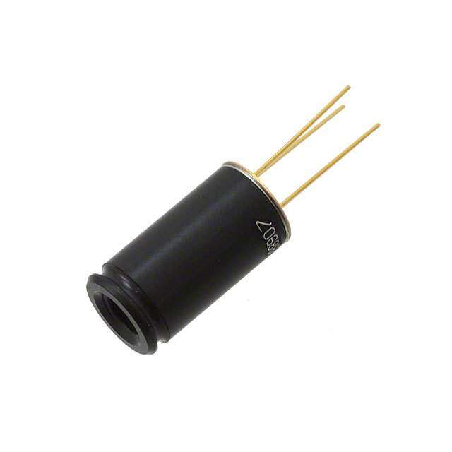
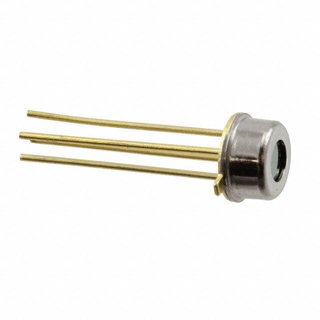
| 描述 | IC DGTL THERM SNSR 3.3V SOT23A-5板上安装温度传感器 Digital Thermal |
| 产品分类 | |
| 品牌 | Microchip Technology |
| 产品手册 | |
| 产品图片 |
|
| rohs | 符合RoHS无铅 / 符合限制有害物质指令(RoHS)规范要求 |
| 产品系列 | 板上安装温度传感器,Microchip Technology TC74A5-3.3VCTTR- |
| 数据手册 | http://www.microchip.com/mymicrochip/filehandler.aspx?ddocname=en011621 |
| 产品型号 | TC74A5-3.3VCTTR |
| 产品目录页面 | |
| 产品种类 | 板上安装温度传感器 |
| 传感器类型 | 内部 |
| 供应商器件封装 | SOT-23-5 |
| 关闭 | Shutdown |
| 其它名称 | TC74A5-3.3VCTCT |
| 准确性 | +/- 3 C |
| 功能 | 温度监控系统(传感器) |
| 包装 | 剪切带 (CT) |
| 商标 | Microchip Technology |
| 安装类型 | 表面贴装 |
| 封装 | Reel |
| 封装/外壳 | SC-74A,SOT-753 |
| 封装/箱体 | SOT-23-5 |
| 工作温度 | -40°C ~ 125°C |
| 工厂包装数量 | 3000 |
| 感应温度 | -40°C ~ 125°C |
| 拓扑 | ADC(三角积分型),寄存器库 |
| 数字输出-位数 | 8 bit |
| 数字输出-总线接口 | 2-Wire, I2C, SMBus |
| 最大工作温度 | + 125 C |
| 最小工作温度 | - 40 C |
| 标准包装 | 1 |
| 电压-电源 | 2.7 V ~ 5.5 V |
| 电源电压-最大 | 5.5 V |
| 电源电压-最小 | 2.7 V |
| 电源电流 | 350 uA |
| 精度 | ±3°C(最大) |
| 设备功能 | Sensor |
| 输出报警 | 无 |
| 输出电流 | +/- 50 mA |
| 输出类型 | I²C/SMBus |
| 输出风扇 | 无 |
| 配置 | Local |


- 商务部:美国ITC正式对集成电路等产品启动337调查
- 曝三星4nm工艺存在良率问题 高通将骁龙8 Gen1或转产台积电
- 太阳诱电将投资9.5亿元在常州建新厂生产MLCC 预计2023年完工
- 英特尔发布欧洲新工厂建设计划 深化IDM 2.0 战略
- 台积电先进制程称霸业界 有大客户加持明年业绩稳了
- 达到5530亿美元!SIA预计今年全球半导体销售额将创下新高
- 英特尔拟将自动驾驶子公司Mobileye上市 估值或超500亿美元
- 三星加码芯片和SET,合并消费电子和移动部门,撤换高东真等 CEO
- 三星电子宣布重大人事变动 还合并消费电子和移动部门
- 海关总署:前11个月进口集成电路产品价值2.52万亿元 增长14.8%


PDF Datasheet 数据手册内容提取
M TC74 Tiny Serial Digital Thermal Sensor Features General Description • Digital Temperature Sensing in SOT-23-5 or The TC74 is a serially accessible, digital temperature TO-220 Packages sensor particularly suited for low cost and small form- • Outputs Temperature as an 8-Bit Digital Word factor applications. Temperature data is converted from • Simple SMBus/I2C™ Serial Port Interface the onboard thermal sensing element and made available as an 8-bit digital word. • Solid-State Temperature Sensing: Communication with the TC74 is accomplished via a 2- - ±2°C (max.) Accuracy from +25°C to +85°C wire SMBus/I2C compatible serial port. This bus also - ±3°C (max.) Accuracy from 0°C to +125°C can be used to implement multi-drop/multi-zone • Supply Voltage of 2.7V to 5.5V monitoring. The SHDN bit in the CONFIG register can • Low Power: be used to activate the low power Standby mode. - 200µA (typ.) Operating Current Temperature resolution is 1°C. Conversion rate is a - 5µA (typ.) Standby Mode Current nominal 8 samples/sec. During normal operation, the quiescent current is 200µA (typ). During standby Applications operation, the quiescent current is 5µA (typ). • Thermal Protection for Hard Disk Drives Small size, low installed cost and ease of use make the and other PC Peripherals TC74 an ideal choice for implementing thermal management in a variety of systems. • PC Card Devices for Notebook Computers • Low Cost Thermostat Controls Functional Block Diagram • Power Supplies • Thermistor Replacement Package Types Internal Sensor SDA (Diode) Serial Port Interface TO-220 SOT-23 SCLK SDA SCLK ∆Σ Modulator 5 4 TC74 Control Logic 12 3 45 TC74 1 2 3 NC GND V Temperature CADKD DD NDNLD Register SGCV S Note: The TO-220 tab is connected to pin 3 (GND) 2002 Microchip Technology Inc. DS21462C-page 1
TC74 1.0 ELECTRICAL † Notice: Stresses above those listed under "Maxi- CHARACTERISTICS mum Ratings" may cause permanent damage to the device. This is a stress rating only and functional oper- ation of the device at those or any other conditions 1.1 Absolute Maximum Ratings† above those indicated in the operation listings of this Supply Voltage (V )............................................ +6V specification is not implied. Exposure to maximum rat- DD ing conditions for extended periods may affect device Voltage On Any Pin.......(GND – 0.3V) to (V + 0.3V) DD reliability. Current On Any Pin..........................................±50mA Operating Temperature (T )........-40°C ≤ T ≤ +125°C A A Storage Temperature (T )..............-65°C to +150°C STG Junction Temperature (T )................................+150°C J DC CHARACTERISTICS Electrical Specifications: Unless otherwise noted, V = 3.3V for TC74AX-3.3VXX and DD V = 5.0V for TC74AX-5.0VXX, -40°C ≤ T ≤ 125°C. Note5 DD A Parameters Sym Min Typ Max Units Conditions Power Supply Power-on Reset Threshold V 1.2 — 2.2 V V Falling Edge or Rising POR DD Edge Supply Voltage V 2.7 — 5.5 V Note5 DD Operating Current I — 200 350 µA V = 5.5V, Note1 DD DD Standby Supply Current I — 5.0 10 µA V = 3.3V DD-STANDBY DD Serial Port Inactive, Note4 Temperature-to-Bits Converter Temperature Accuracy T -2.0 — +2.0 °C +25°C <T < +85°C ERR A -3.0 — +3.0 0°C < T < +125°C A — ±2.0 — -40°C < T < 0°C A Conversion Rate CR 4 8 — SPS Note2 Serial Port Interface Logic Input High V 0.8 x V — — V IH DD Logic Input Low V — — 0.2 x V V IL DD SDA Output Low V — — 0.4 V I = 3mA OL OL — — 0.6 V I = 6mA, Note3 OL Input Capacitance SDA, SCLK C — 5.0 — pF IN I/O Leakage I -1.0 0.1 1.0 µA LEAK Serial Port AC Timing (C = 80pF) LOAD SMBus/I2C Clock Frequency f 10 — 100 kHz SMB Low Clock Period t 4.7 — — µsec 10% to 10% LOW High Clock Period t 4.0 — — µsec 90% to 90% HIGH Note 1: Operating current is an average value integrated over multiple conversion cycles. Transient current may exceed this specification. 2: Maximum ensured conversion time after Power-on Reset (POR to DATA_RDY) is 250msec. 3: Output current should be minimized for best temperature accuracy. Power dissipation within the TC74 will cause self-heating and temperature drift error. 4: SDA and SCLK must be connected to V or GND. DD 5: V = 3.3V for TC74AX -3.3VXX. V = 5.0V for TC74AX -5.0VXX. All part types of the TC74 will operate DD DD properly over the wider power supply range of 2.7V to 5.5V. Each part type is tested and specified for rated accuracy at its nominal supply voltage. As V varies from the nominal value, accuracy will degrade 1°C/V DD of V change. DD DS21462C-page 2 2002 Microchip Technology Inc.
TC74 DC CHARACTERISTICS (CONTINUED) Electrical Specifications: Unless otherwise noted, V = 3.3V for TC74AX-3.3VXX and DD V = 5.0V for TC74AX-5.0VXX, -40°C ≤ T ≤ 125°C. Note5 DD A Parameters Sym Min Typ Max Units Conditions SMBus/I2C Rise Time t — — 1000 nsec 10% to 90% R SMBus/I2C Fall Time t — — 300 nsec 90% to10% F START Condition Setup Time t 4.0 — — µsec 90% SCLK to 10% SDA SU(START) (for repeated START Condition) START Condition Hold Time t 4.0 — — µsec H(START) Data In Setup Time t 1000 — — nsec SU-DATA Data In Hold Time t 1250 — — nsec H-DAT STOP Condition Setup Time t 4.0 — — µsec SU(STOP) Bus Free Time Prior to New t 4.7 — — µsec IDLE Transition Power-on Reset Delay t — 500 — µsec V ≥ V (Rising Edge) POR DD POR Note 1: Operating current is an average value integrated over multiple conversion cycles. Transient current may exceed this specification. 2: Maximum ensured conversion time after Power-on Reset (POR to DATA_RDY) is 250msec. 3: Output current should be minimized for best temperature accuracy. Power dissipation within the TC74 will cause self-heating and temperature drift error. 4: SDA and SCLK must be connected to V or GND. DD 5: V = 3.3V for TC74AX -3.3VXX. V = 5.0V for TC74AX -5.0VXX. All part types of the TC74 will operate DD DD properly over the wider power supply range of 2.7V to 5.5V. Each part type is tested and specified for rated accuracy at its nominal supply voltage. As V varies from the nominal value, accuracy will degrade 1°C/V DD of V change. DD 2002 Microchip Technology Inc. DS21462C-page 3
TC74 SMBUS Read Timing Diagram A B C D E F G H I J K t t LOW HIGH SCLK SDA t t t t t SU(START) H(START) SU-DATA SU(STOP) IDLE A = Start Condition E = Slave Pulls SDA Line Low I = Acknowledge Clock Pulse B = MSB of Address Clocked into Slave F = Acknowledge Bit Clocked into Master J = Stop Condition C = LSB of Address Clocked into Slave G = MSB of Data Clocked into Master K = New Start Condition D = R/W Bit Clocked into Slave H = LSB of Data Clocked into Master SMBUS Write Timing Diagram A B C D E F G H I J K L M t t LOW HIGH SCLK SDA t t t t t t SU(START) H(START) SU-DATA H-DATA SU(STOP) IDLE A = Start Condition F = Acknowledge Bit Clocked into Master J = Acknowledge Clocked into Master B = MSB of Address Clocked into Slave G = MSB of Data Clocked into Slave K = Acknowledge Clock Pulse C = LSB of Address Clocked into Slave H = LSB of Data Clocked into Slave L = Stop Condition, Data Executed by Slave D = R/W Bit Clocked into Slave I = Slave Pulls SDA Line Low M = New Start Condition E = Slave Pulls SDA Line Low FIGURE 1-1: Timing Diagrams. DS21462C-page 4 2002 Microchip Technology Inc.
TC74 2.0 PIN DESCRIPTIONS The descriptions of the pins are listed in Table2-1. TABLE 2-1: PIN FUNCTION TABLE Pin No. Pin No. (5-Pin Symbol Type Description (5-Pin TO-220) SOT-23) 1 1 NC None No Internal Connection 2 3 GND Power System Ground 3 5 V Power Power Supply Input DD 4 4 SCLK Input SMBus/I2C Serial Clock 5 2 SDA Bidirectional SMBus/I2C Serial Data 2.1 Ground (GND) Input. Ground return for all TC74 functions. 2.2 Power Supply Input (V ) DD Power supply input. See Electrical Specifications. 2.3 SMBus/I2C Serial Clock (SCLK) Input. SMBus/I2C serial clock. Clocks data into and out of the TC74. See System Management Bus Specification, Rev. 1.0, for timing diagrams. 2.4 Serial Data (SDA) Bidirectional. Serial data is transferred on the SMBus/ I2C in both directions using this pin. See System Management Bus Specification, Rev. 1.0 for timing diagrams. 2002 Microchip Technology Inc. DS21462C-page 5
TC74 3.0 DETAILED DESCRIPTION TABLE 3-2: SERIAL BUS CONVENTIONS Term Explanation 3.1 Functional Description Transmitter The device sending data to the bus. The TC74 acquires and converts temperature Receiver The device receiving data from the bus. information from its onboard solid-state sensor with a Master The device which controls the bus initi- resolution of ±1°C. It stores the data in an internal ating transfers (START), generating the register which is then read through the serial port. The system interface is a slave SMBus/I2C port, through clock and terminating transfers (STOP). which temperature data can be read at any time. Eight SMBus/I2C addresses are programmable for the TC74, Slave The device addressed by the master. which allows for a multi-sensor configuration. Also, START A unique condition signaling the begin- there is low power Standby mode when temperature ning of a transfer indicated by SDA acquisition is suspended. falling (high-low) while SCLK is high. STOP A unique condition signaling the end of 3.1.1 STANDBY MODE a transfer indicated by SDA rising (low- The host is allowed, by the TC74, to put it into a low high) while SCLK is high. power (IDD = 5µA, typical) Standby mode. In this ACK A Receiver acknowledges the receipt mode, the A/D converter is halted and the temperature of each byte with this unique condition. data registers are frozen. The SMBus/I2C port, though, The Receiver drives SDA low during operates normally. Standby mode is enabled by setting SCLK high of the ACK clock-pulse. The the SHDN bit in the CONFIG register. Table3-1 Master provides the clock pulse for the summarizes this operation. ACK cycle. Busy Communication is not possible TABLE 3-1: STANDBY MODE OPERATION because the bus is in use. SHDN Bit Operating Mode NOT Busy When the bus is idle, both SDA and 0 Normal SCLK will remain high. 1 Standby Data Valid The state of SDA must remain stable during the high period of SCLK in order 3.1.2 SMBUS/I2C SLAVE ADDRESS for a data bit to be considered valid. SDA only changes state while SCLK is The TC74 is internally programmed to have a default low during normal data transfers (see SMBus/I2C address value of 1001 101b. Seven other START and STOP conditions). addresses are available by custom order (contact Microchip Technology Inc. All transfers take place under the control of a host, usu- ally a CPU or microcontroller, acting as the Master. This 3.2 Serial Port Operation host provides the clock signal for all transfers. The TC74 always operates as a Slave. The serial protocol The Serial Clock input (SCLK) and bidirectional data is illustrated in Figure3-1. All data transfers have two port (SDA) form a 2-wire bidirectional serial port for pro- phases and all bytes are transferred MSB first. gramming and interrogating the TC74. The Accesses are initiated by a START condition, followed conventions used in this bus architecture are listed in by a device address byte and one or more data bytes. Table3-2. The device address byte includes a Read/Write selec- tion bit. Each access must be terminated by a STOP condition. A convention called “Acknowledge” (ACK) confirms receipt of each byte. Note that SDA can change only during periods when SCLK is low (SDA changes while SCLK is high are reserved for START and STOP conditions). DS21462C-page 6 2002 Microchip Technology Inc.
TC74 Write Byte Format S Address WR ACK Command ACK Data ACK P 7 Bits 8 Bits 8 Bits Slave Address Command Byte: selects Data Byte: data goes which register you are into the register set writing to. by the command byte. Read Byte Format S Address WR ACK Command ACK S Address RD ACK Data NACK P 7 Bits 8 Bits 7 Bits 8 Bits Slave Address Command Byte: selects Slave Address: repeated Data Byte: reads from which register you are due to change in data- the register set by the reading from. flow direction. command byte. Receive Byte Format S Address RD ACK Data NACK P 7 Bits 8 Bits S = START Condition Data Byte: reads data from P = STOP Condition the register commanded by Shaded = Slave Transmission the last Read Byte or Write Byte transmission. FIGURE 3-1: SMBus/I2C Protocols. 3.3 START Condition (S) 3.6 Data Byte The TC74 continuously monitors the SDA and SCLK After a successful ACK of the address byte, the host lines for a START condition (a high-to-low transition of must transmit the data byte to be written, or clock-in the SDA while SCLK is high) and will not respond until this data to be read (see the appropriate timing diagrams). condition is met. ACK will be generated upon a successful write of a data byte into the TC74. 3.4 Address Byte 3.7 STOP Condition (P) Immediately following the START condition, the host must transmit the address byte to the TC74. The states Communications must be terminated by a STOP of A2, A1 and A0 determine the SMBus/I2C address for condition (a low-to-high transition of SDA while SCLK the TC74. The 7-bit address transmitted in the serial bit is high). The STOP condition must be communicated stream must match for the TC74 to respond with an by the transmitter to the TC74. Refer to Figure1-1, Acknowledge (indicating the TC74 is on the bus and “Timing Diagrams”, for serial bus timing. ready to accept data). The 8-bit in the address byte is a Read/Write bit. This bit is a ‘1’ for a read operation or ‘0’ for a write operation. During the first phase of any transfer, this bit will be set = 0, indicating that the command byte is being written. 3.5 Acknowledge (ACK) Acknowledge (ACK) provides a positive handshake between the host and the TC74. The host releases SDA after transmitting 8 bits. The host then generates a ninth clock cycle to allow the TC74 to pull the SDA line low. This action acknowledges that the TC74 successfully received the previous 8 bits of data or address. 2002 Microchip Technology Inc. DS21462C-page 7
TC74 4.0 REGISTER SET AND TABLE 4-3: TEMPERATURE REGISTER PROGRAMMER’S MODEL (TEMP) D[7] D[6] D[5] D[4] D[3] D[2] D[1] D[0] TABLE 4-1: COMMAND BYTE MSB X X X X X X LSB DESCRIPTION In temperature data registers, each unit value repre- (SMBUS/I2C READ_BYTE AND sents one degree (Celsius). The value is in 2’s WRITE_BYTE) complement binary format such that a reading of 0000 Command Code Function 0000b corresponds to 0°C. Examples of this temperature to binary value relationship are shown in RTR 00h Read Temperature (TEMP) Table4-4. RWCR 01h Read/Write Configuration (CONFIG) TABLE 4-4: TEMPERATURE-TO-DIGITAL VALUE CONVERSION TABLE 4-2: CONFIGURATION REGISTER (TEMP) (CONFIG); 8 BITS, READ/ Actual Registered Binary WRITE) Temperature Temperature Hex Bit POR Function Type Operation +130.00°C +127°C 0111 1111 D[7] 0 STANDBY Read/ 1 = standby, +127.00°C +127°C 0111 1111 Switch Write 0 = normal +126.50°C +126°C 0111 1110 D[6] 0 Data Ready * Read 1 = ready +25.25°C +25°C 0001 1001 Only 0 = not ready +0.50°C 0°C 0000 0000 D[5]- 0 Reserved - N/A N/A +0.25°C 0°C 0000 0000 D[0] Always returns zero 0.00°C 0°C 0000 0000 when read -0.25°C -1°C 1111 1111 Note 1: *DATA_RDY bit RESET at power-up and -0.50°C -1°C 1111 1111 SHDN enable. -0.75°C -1°C 1111 1111 -1.00°C -1°C 1111 1111 -25.00°C -25°C 1110 0111 -25.25°C -26°C 1110 0110 V DD -54.75°C -55°C 1100 1001 -55.00°C -55°C 1100 1001 -65.00°C -65°C 1011 1111 DATA_RDY 4.2 Register Set Summary The TC74 register set is summarized in Table4-5. All SHDN registers are 8 bits wide. tconv tconv TABLE 4-5: TC74 REGISTER SET FIGURE 4-1: DATA_RDY, SHDN SUMMARY Operation Logic Diagram. POR Name Description Read Write State 4.1 Temperature Register (TEMP), 8 Bits, READ ONLY TEMP Internal Sensor 0000 Temperature (2’s 0000b (1) √ N/A The binary value (2’s complement format) in this regis- Complement) ter represents temperature of the onboard sensor CONFIG CONFIG 0000 following a conversion cycle. The registers are √ √ Register 0000b automatically updated in an alternating manner. Note 1: The TEMP register will be immediately updated by the A/D converter after the DATA_RDY Bit goes high. DS21462C-page 8 2002 Microchip Technology Inc.
TC74 5.0 PACKAGING INFORMATION 5.1 SOT23A Package Marking Information 5-Pin SOT-23A 5 4 1 & 2 = part number code + temp. range and voltage 3 = year and quarter code 1 2 3 4 4 = lot ID number 1 2 3 SOT-23 Package Marking Codes SOT-23 (V) Address Code SOT-23 (V) Address Code TC74A0-3.3VCT 1001 000 V0 TC74A0-5.0VCT 1001 000 U0 TC74A1-3.3VCT 1001 001 V1 TC74A1-5.0VCT 1001 001 U1 TC74A2-3.3VCT 1001 010 V2 TC74A2-5.0VCT 1001 010 U2 TC74A3-3.3VCT 1001 011 V3 TC74A3-5.0VCT 1001 011 U3 TC74A4-3.3VCT 1001 100 V4 TC74A4-5.0VCT 1001 100 U4 TC74A5-3.3VCT 1001 101* V5 TC74A5-5.0VCT 1001 101* U5 TC74A6-3.3VCT 1001 110 V6 TC74A6-5.0VCT 1001 110 U6 TC74A7-3.3VCT 1001 111 V7 TC74A7-5.0VCT 1001 111 U7 Note: * Default Address TO-220 Package Marking Information TO-220 Legend: XX...X Customer specific information* YY Year code (last 2 digits of calendar year) WW Week code (week of January 1 is week ‘01’) NNN Alphanumeric traceability code Note: In the event the full Microchip part number cannot be TC74A0- marked on one line, it will be carried over to the next line thus lim- 3.3VAT iting the number of available characters for customer specific infor- 0229123 mation. 1 2 3 4 5 * Standard marking consists of Microchip part number, year code, week code, and traceability code. 2002 Microchip Technology Inc. DS21462C-page 9
TC74 5.2 Taping Forms Component Taping Orientation for 5-Pin SOT-23A (EIAJ SC-74A) Devices User Direction of Feed Device Marking W PIN 1 P Standard Reel Component Orientation for TR Suffix Device (Mark Right Side Up) Carrier Tape, Number of Components Per Reel and Reel Size: Package Carrier Width (W) Pitch (P) Part Per Full Reel Reel Size 5-Pin SOT-23A 8 mm 4 mm 3000 7 in. DS21462C-page 10 2002 Microchip Technology Inc.
TC74 5.3 Package Dimensions SOT-23A-5 .075 (1.90) REF. .122 (3.10) .071 (1.80) .098 (2.50) .059 (1.50) .020 (0.50) .012 (0.30) .037 (0.95) PIN 1 REF. .118 (3.00) .010 (2.80) .057 (1.45) .035 (0.90) .010 (0.25) 10° MAX. .004 (0.09) .006 (0.15) .024 (0.60) .000 (0.00) .004 (0.10) Dimensions: inches (mm) 5-Pin TO-220 .185 (4.70) .165 (4.19) .415 (10.54) .117 (2.97) .390 (9.91) .156 (3.96) .055 (1.40) .103 (2.62) .045 (1.14) .140 (3.56) DIA. .293 (7.44) .204 (5.18) 3 - 7.5 .613 (15.57) 5 PLCS. .569 (14.45) .037 (0.95) .590 (14.99) .025 (0.64) .482 (12.24) .025 (0.64) .012 (0.30) PIN 1 .072 (1.83) .062 (1.57) .115 (2.92) .273 (6.93) .087 (2.21) .263 (6.68) Dimensions: inches (mm) 2002 Microchip Technology Inc. DS21462C-page 11
TC74 NOTES: DS21462C-page 12 2002 Microchip Technology Inc.
TC74 PRODUCT IDENTIFICATION SYSTEM To order or obtain information, e.g., on pricing or delivery, refer to the factory or the listed sales office. PART NO. XX -XX X XX Examples: a) TC74A0-3.3VCTTR: SOT-23 Serial Digital Thermal Sensor Device Address Supply Operating Package b) TC74A1-3.3VCTTR: SOT-23 Serial Digital Thermal Sensor Options Voltage Temperature c) TC74A2-3.3VCTTR: SOT-23 Serial Digital Thermal Sensor d) TC74A3-3.3VCTTR: SOT-23 Serial Digital Thermal Sensor Device: TC74: Serial Digital Thermal Sensor e) TC74A4-3.3VCTTR: SOT-23 Serial Digital Thermal Sensor f) TC74A5-3.3VCTTR: SOT-23 Serial Digital Thermal Sensor * Address Options: A0 = 1001 000 A1 = 1001 001 g) TC74A6-3.3VCTTR: SOT-23 Serial Digital Thermal Sensor A2 = 1001 010 h) TC74A7-3.3VCTTR: SOT-23 Serial Digital Thermal Sensor A3 = 1001 011 A4 = 1001 100 A5 = 1001 101 * a) TC74A0-5.0VCTTR: SOT-23 Serial Digital Thermal Sensor A6 = 1001 110 b) TC74A1-5.0VCTTR: SOT-23 Serial Digital Thermal Sensor A7 = 1001 111 c) TC74A2-5.0VCTTR: SOT-23 Serial Digital Thermal Sensor * Default Address d) TC74A3-5.0VCTTR: SOT-23 Serial Digital Thermal Sensor e) TC74A4-5.0VCTTR: SOT-23 Serial Digital Thermal Sensor Supply Voltage: 3.3 = Accuracy optimized for 3.3V f) TC74A5-5.0VCTTR: SOT-23 Serial Digital Thermal Sensor * 5.0 = Accuracy optimized for 5.0V g) TC74A6-5.0VCTTR: SOT-23 Serial Digital Thermal Sensor h) TC74A7-5.0VCTTR: SOT-23 Serial Digital Thermal Sensor Operating Temperature: V = -40°C ≤ TA ≤ +125°C * Default Address Package: CTTR = SOT-23-5 (Tape and Reel only) PART NO. XX -XX X XX Examples: a) TC74A0-3.3VAT: TO-220 Serial Digital Thermal Sensor Device Address Supply Operating Package b) TC74A1-3.3VAT: TO-220 Serial Digital Thermal Sensor Options Voltage Temperature c) TC74A2-3.3VAT: TO-220 Serial Digital Thermal Sensor d) TC74A3-3.3VAT: TO-220 Serial Digital Thermal Sensor Device: TC74: Serial Digital Thermal Sensor e) TC74A4-3.3VAT: TO-220 Serial Digital Thermal Sensor f) TC74A5-3.3VAT: TO-220 Serial Digital Thermal Sensor * Address Options: A0 = 1001 000 A1 = 1001 001 g) TC74A6-3.3VAT: TO-220 Serial Digital Thermal Sensor A2 = 1001 010 h) TC74A7-3.3VAT: TO-220 Serial Digital Thermal Sensor A3 = 1001 011 A4 = 1001 100 A5 = 1001 101 * a) TC74A0-5.0VAT: TO-220 Serial Digital Thermal Sensor A6 = 1001 110 b) TC74A1-5.0VAT: TO-220 Serial Digital Thermal Sensor A7 = 1001 111 c) TC74A2-5.0VAT: TO-220 Serial Digital Thermal Sensor * Default Address d) TC74A3-5.0VAT: TO-220 Serial Digital Thermal Sensor e) TC74A4-5.0VAT: TO-220 Serial Digital Thermal Sensor Output Voltage: 3.3 = Accuracy optimized for 3.3V f) TC74A5-5.0VAT: TO-220 Serial Digital Thermal Sensor * 5.0 = Accuracy optimized for 5.0V g) TC74A6-5.0VAT: TO-220 Serial Digital Thermal Sensor h) TC74A7-5.0VAT: TO-220 Serial Digital Thermal Sensor Operating Temperature: V = -40°C ≤ T ≤ +125°C A * Default Address Package: AT = TO-220-5 Sales and Support Data Sheets Products supported by a preliminary Data Sheet may have an errata sheet describing minor operational differences and recom- mended workarounds. To determine if an errata sheet exists for a particular device, please contact one of the following: 1. Your local Microchip sales office 2. The Microchip Corporate Literature Center U.S. FAX: (480) 792-7277 3. The Microchip Worldwide Site (www.microchip.com) Please specify which device, revision of silicon and Data Sheet (include Literature #) you are using. New Customer Notification System Register on our web site (www.microchip.com/cn) to receive the most current information on our products. 2002 Microchip Technology Inc. DS21462C-page13
TC74 NOTES: DS21462C-page 14 2002 Microchip Technology Inc.
Note the following details of the code protection feature on Microchip devices: • Microchip products meet the specification contained in their particular Microchip Data Sheet. • Microchip believes that its family of products is one of the most secure families of its kind on the market today, when used in the intended manner and under normal conditions. • There are dishonest and possibly illegal methods used to breach the code protection feature. All of these methods, to our knowl- edge, require using the Microchip products in a manner outside the operating specifications contained in Microchip's Data Sheets. Most likely, the person doing so is engaged in theft of intellectual property. • Microchip is willing to work with the customer who is concerned about the integrity of their code. • Neither Microchip nor any other semiconductor manufacturer can guarantee the security of their code. Code protection does not mean that we are guaranteeing the product as “unbreakable.” Code protection is constantly evolving. We at Microchip are committed to continuously improving the code protection features of our products. Information contained in this publication regarding device Trademarks applications and the like is intended through suggestion only and may be superseded by updates. It is your responsibility to The Microchip name and logo, the Microchip logo, KEELOQ, ensure that your application meets with your specifications. MPLAB, PIC, PICmicro, PICSTART and PRO MATE are No representation or warranty is given and no liability is registered trademarks of Microchip Technology Incorporated assumed by Microchip Technology Incorporated with respect in the U.S.A. and other countries. to the accuracy or use of such information, or infringement of FilterLab, microID, MXDEV, MXLAB, PICMASTER, SEEVAL patents or other intellectual property rights arising from such and The Embedded Control Solutions Company are use or otherwise. Use of Microchip’s products as critical com- registered trademarks of Microchip Technology Incorporated ponents in life support systems is not authorized except with in the U.S.A. express written approval by Microchip. No licenses are con- veyed, implicitly or otherwise, under any intellectual property dsPIC, dsPICDEM.net, ECONOMONITOR, FanSense, rights. FlexROM, fuzzyLAB, In-Circuit Serial Programming, ICSP, ICEPIC, microPort, Migratable Memory, MPASM, MPLIB, MPLINK, MPSIM, PICC, PICDEM, PICDEM.net, rfPIC, Select Mode and Total Endurance are trademarks of Microchip Technology Incorporated in the U.S.A. and other countries. Serialized Quick Turn Programming (SQTP) is a service mark of Microchip Technology Incorporated in the U.S.A. All other trademarks mentioned herein are property of their respective companies. © 2002, Microchip Technology Incorporated, Printed in the U.S.A., All Rights Reserved. Printed on recycled paper. Microchip received QS-9000 quality system certification for its worldwide headquarters, design and wafer fabrication facilities in Chandler and Tempe, Arizona in July 1999 and Mountain View, California in March 2002. The Company’s quality system processes and procedures are QS-9000 compliant for its PICmicro® 8-bit MCUs, KEELOQ® code hopping devices, Serial EEPROMs, microperipherals, non-volatile memory and analog products. In addition, Microchip’s quality system for the design and manufacture of development systems is ISO 9001 certified. 2002 Microchip Technology Inc. DS21462C - page 15
M WORLDWIDE SALES AND SERVICE AMERICAS ASIA/PACIFIC Japan Corporate Office Australia Microchip Technology Japan K.K. Benex S-1 6F 2355 West Chandler Blvd. Microchip Technology Australia Pty Ltd 3-18-20, Shinyokohama Chandler, AZ 85224-6199 Suite 22, 41 Rawson Street Kohoku-Ku, Yokohama-shi Tel: 480-792-7200 Fax: 480-792-7277 Epping 2121, NSW Kanagawa, 222-0033, Japan Technical Support: 480-792-7627 Australia Tel: 81-45-471- 6166 Fax: 81-45-471-6122 Web Address: http://www.microchip.com Tel: 61-2-9868-6733 Fax: 61-2-9868-6755 Korea Rocky Mountain China - Beijing Microchip Technology Korea 2355 West Chandler Blvd. Microchip Technology Consulting (Shanghai) 168-1, Youngbo Bldg. 3 Floor Chandler, AZ 85224-6199 Co., Ltd., Beijing Liaison Office Samsung-Dong, Kangnam-Ku Tel: 480-792-7966 Fax: 480-792-4338 Unit 915 Seoul, Korea 135-882 Bei Hai Wan Tai Bldg. Atlanta Tel: 82-2-554-7200 Fax: 82-2-558-5934 No. 6 Chaoyangmen Beidajie 500 Sugar Mill Road, Suite 200B Beijing, 100027, No. China Singapore Atlanta, GA 30350 Tel: 86-10-85282100 Fax: 86-10-85282104 Microchip Technology Singapore Pte Ltd. Tel: 770-640-0034 Fax: 770-640-0307 200 Middle Road China - Chengdu Boston Microchip Technology Consulting (Shanghai) #07-02 Prime Centre Singapore, 188980 2 Lan Drive, Suite 120 Co., Ltd., Chengdu Liaison Office Tel: 65-6334-8870 Fax: 65-6334-8850 Westford, MA 01886 Rm. 2401, 24th Floor, Tel: 978-692-3848 Fax: 978-692-3821 Ming Xing Financial Tower Taiwan Microchip Technology (Barbados) Inc., Chicago No. 88 TIDU Street Chengdu 610016, China Taiwan Branch 333 Pierce Road, Suite 180 Tel: 86-28-86766200 Fax: 86-28-86766599 11F-3, No. 207 Itasca, IL 60143 Tung Hua North Road Tel: 630-285-0071 Fax: 630-285-0075 China - Fuzhou Taipei, 105, Taiwan Dallas Microchip Technology Consulting (Shanghai) Tel: 886-2-2717-7175 Fax: 886-2-2545-0139 Co., Ltd., Fuzhou Liaison Office 4570 Westgrove Drive, Suite 160 Unit 28F, World Trade Plaza EUROPE Addison, TX 75001 Tel: 972-818-7423 Fax: 972-818-2924 No. 71 Wusi Road Austria Fuzhou 350001, China Detroit Tel: 86-591-7503506 Fax: 86-591-7503521 Microchip Technology Austria GmbH Durisolstrasse 2 Tri-Atria Office Building China - Shanghai A-4600 Wels 32255 Northwestern Highway, Suite 190 Microchip Technology Consulting (Shanghai) Farmington Hills, MI 48334 Co., Ltd. ATeuls: t4ri3a-7242-2244-399 Tel: 248-538-2250 Fax: 248-538-2260 Room 701, Bldg. B Fax: 43-7242-2244-393 Kokomo Far East International Plaza Denmark 2767 S. Albright Road No. 317 Xian Xia Road Microchip Technology Nordic ApS Kokomo, Indiana 46902 Shanghai, 200051 Regus Business Centre Tel: 765-864-8360 Fax: 765-864-8387 Tel: 86-21-6275-5700 Fax: 86-21-6275-5060 Lautrup hoj 1-3 Los Angeles China - Shenzhen Ballerup DK-2750 Denmark 18201 Von Karman, Suite 1090 Microchip Technology Consulting (Shanghai) Tel: 45 4420 9895 Fax: 45 4420 9910 Irvine, CA 92612 Co., Ltd., Shenzhen Liaison Office France Rm. 1315, 13/F, Shenzhen Kerry Centre, Tel: 949-263-1888 Fax: 949-263-1338 Microchip Technology SARL Renminnan Lu Parc d’Activite du Moulin de Massy San Jose Shenzhen 518001, China 43 Rue du Saule Trapu Microchip Technology Inc. Tel: 86-755-82350361 Fax: 86-755-82366086 Batiment A - ler Etage 2107 North First Street, Suite 590 China - Hong Kong SAR 91300 Massy, France San Jose, CA 95131 Microchip Technology Hongkong Ltd. Tel: 33-1-69-53-63-20 Fax: 33-1-69-30-90-79 Tel: 408-436-7950 Fax: 408-436-7955 Unit 901-6, Tower 2, Metroplaza Germany Toronto 223 Hing Fong Road Microchip Technology GmbH 6285 Northam Drive, Suite 108 Kwai Fong, N.T., Hong Kong Steinheilstrasse 10 Mississauga, Ontario L4V 1X5, Canada Tel: 852-2401-1200 Fax: 852-2401-3431 D-85737 Ismaning, Germany Tel: 905-673-0699 Fax: 905-673-6509 India Tel: 49-89-627-144 0 Fax: 49-89-627-144-44 Microchip Technology Inc. Italy India Liaison Office Microchip Technology SRL Divyasree Chambers Centro Direzionale Colleoni 1 Floor, Wing A (A3/A4) Palazzo Taurus 1 V. Le Colleoni 1 No. 11, O’Shaugnessey Road 20041 Agrate Brianza Bangalore, 560 025, India Milan, Italy Tel: 91-80-2290061 Fax: 91-80-2290062 Tel: 39-039-65791-1 Fax: 39-039-6899883 United Kingdom Microchip Ltd. 505 Eskdale Road Winnersh Triangle Wokingham Berkshire, England RG41 5TU Tel: 44 118 921 5869 Fax: 44-118 921-5820 10/18/02 DS21462C-page 16 2002 Microchip Technology Inc.
Mouser Electronics Authorized Distributor Click to View Pricing, Inventory, Delivery & Lifecycle Information: M icrochip: TC74A1-5.0VAT TC74A1-5.0VCTTR TC74A2-3.3VAT TC74A2-3.3VCTTR TC74A3-3.3VAT TC74A3-3.3VCTTR TC74A3-5.0VAT TC74A4-3.3VAT TC74A5-3.3VAT TC74A5-5.0VCTTR TC74A6-5.0VCTTR TC74A7-5.0VCTTR TC74A0-3.3VAT TC74A0-5.0VAT TC74A3-5.0VCTTR TC74A4-5.0VAT TC74A5-3.3VCTTR TC74A5-5.0VAT TC74A7-5.0VAT TC74A0-3.3VCTTR TC74A0-5.0VCTTR TC74A1-3.3VAT TC74A1-3.3VCTTR TC74A2-5.0VAT TC74A2-5.0VCTTR TC74A4-3.3VCTTR TC74A6-3.3VAT TC74A6-3.3VCTTR TC74A7-3.3VAT TC74A4-5.0VCTTR TC74A6-5.0VAT TC74A7-3.3VCTTR