ICGOO在线商城 > 集成电路(IC) > PMIC - 电机驱动器,控制器 > TC648VOA
- 型号: TC648VOA
- 制造商: Microchip
- 库位|库存: xxxx|xxxx
- 要求:
| 数量阶梯 | 香港交货 | 国内含税 |
| +xxxx | $xxxx | ¥xxxx |
查看当月历史价格
查看今年历史价格
TC648VOA产品简介:
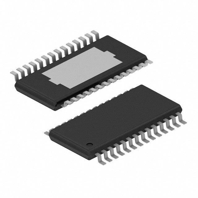
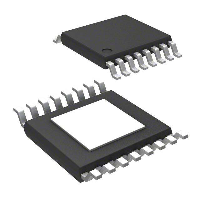
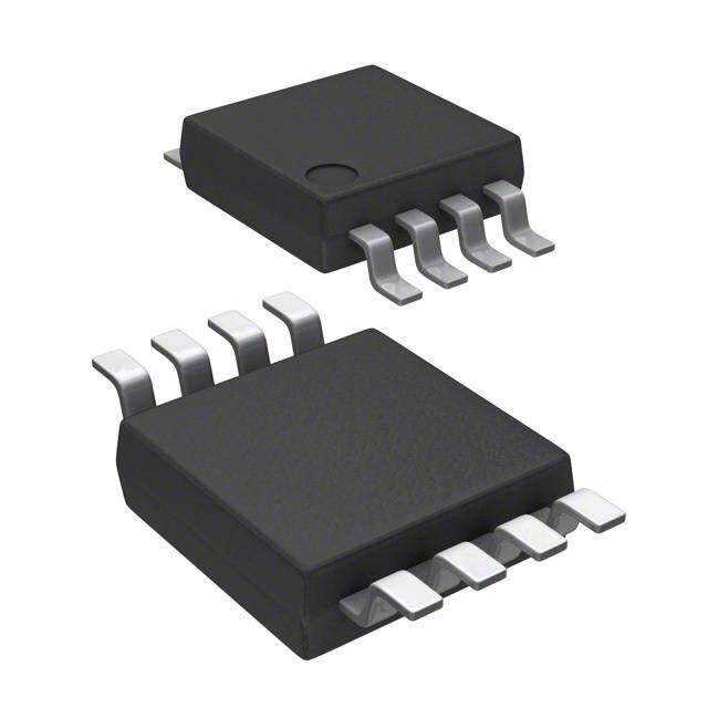
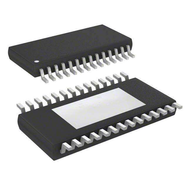
ICGOO电子元器件商城为您提供TC648VOA由Microchip设计生产,在icgoo商城现货销售,并且可以通过原厂、代理商等渠道进行代购。 TC648VOA价格参考。MicrochipTC648VOA封装/规格:PMIC - 电机驱动器,控制器, 电机驱动器 并联 8-SOIC。您可以下载TC648VOA参考资料、Datasheet数据手册功能说明书,资料中有TC648VOA 详细功能的应用电路图电压和使用方法及教程。
| 参数 | 数值 |
| 产品目录 | 集成电路 (IC)半导体 |
| 描述 | IC MOTOR CONTROLLER PAR 8SOIC马达/运动/点火控制器和驱动器 Shtdn & Over-T Alert |
| 产品分类 | PMIC - 电机, 电桥式驱动器集成电路 - IC |
| 品牌 | Microchip Technology |
| 产品手册 | |
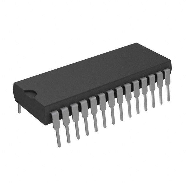
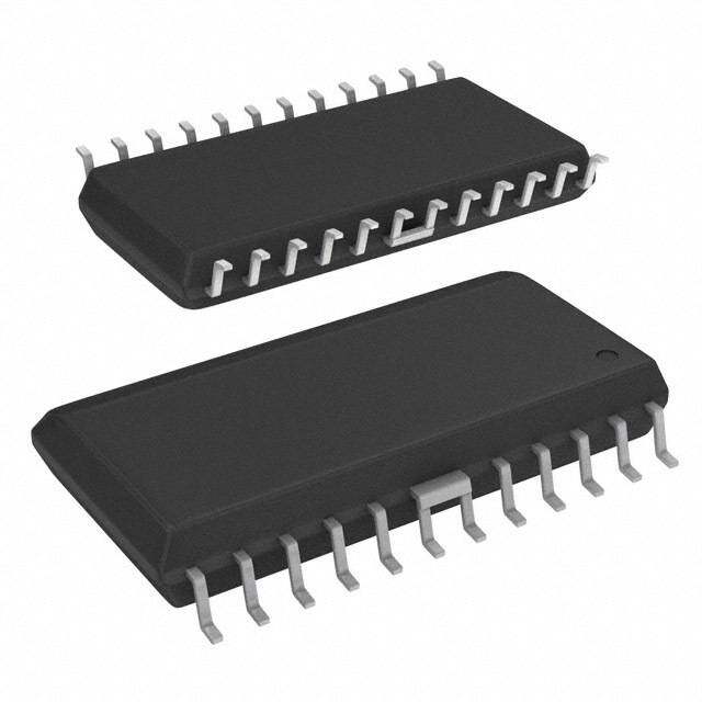
| 产品图片 |
|
| rohs | 符合RoHS无铅 / 符合限制有害物质指令(RoHS)规范要求 |
| 产品系列 | 电源管理 IC,马达/运动/点火控制器和驱动器,Microchip Technology TC648VOA- |
| 数据手册 | http://www.microchip.com/mymicrochip/filehandler.aspx?ddocname=en011603 |
| 产品型号 | TC648VOA |
| 产品 | Fan / Motor Controllers / Drivers |
| 产品种类 | 马达/运动/点火控制器和驱动器 |
| 供应商器件封装 | 8-SOIC N |
| 关闭阈值 | 2.8 V |
| 功能 | 控制器 - 换向,方向管理 |
| 包装 | 管件 |
| 商标 | Microchip Technology |
| 安装类型 | 表面贴装 |
| 安装风格 | SMD/SMT |
| 封装 | Tube |
| 封装/外壳 | 8-SOIC(0.154",3.90mm 宽) |
| 封装/箱体 | SOIC-8 |
| 工作温度 | 0 C to + 85 C |
| 工作电源电压 | 3 V to 5.5 V |
| 工厂包装数量 | 100 |
| 应用 | 风扇控制器 |
| 接口 | 并联 |
| 标准包装 | 100 |
| 电压-电源 | 3 V ~ 5.5 V |
| 电压-负载 | - |
| 电机类型-AC,DC | 无刷 DC(BLDC) |
| 电机类型-步进 | - |
| 电流-输出 | - |
| 电源电流 | 1 mA |
| 类型 | Controller - PWM Fan |
| 输出配置 | 前级驱动器 |






- 商务部:美国ITC正式对集成电路等产品启动337调查
- 曝三星4nm工艺存在良率问题 高通将骁龙8 Gen1或转产台积电
- 太阳诱电将投资9.5亿元在常州建新厂生产MLCC 预计2023年完工
- 英特尔发布欧洲新工厂建设计划 深化IDM 2.0 战略
- 台积电先进制程称霸业界 有大客户加持明年业绩稳了
- 达到5530亿美元!SIA预计今年全球半导体销售额将创下新高
- 英特尔拟将自动驾驶子公司Mobileye上市 估值或超500亿美元
- 三星加码芯片和SET,合并消费电子和移动部门,撤换高东真等 CEO
- 三星电子宣布重大人事变动 还合并消费电子和移动部门
- 海关总署:前11个月进口集成电路产品价值2.52万亿元 增长14.8%
PDF Datasheet 数据手册内容提取
M TC648 Fan Speed Controller with Auto-Shutdown and Over-Temperature Alert Features Package Types • Temperature Proportional Fan Speed for Acoustic SOIC/PDIP/MSOP Control and Longer Fan Life • Efficient PWM Fan Drive VIN 1 8 VDD • 3.0V to 5.5V Supply Range: CF 2 7 VOUT TC648 - Fan Voltage Independent of TC648 VAS 3 6 OTF Supply Voltage - Supports any Fan Voltage GND 4 5 NC • Over-temperature Fault Detection • Automatic Shutdown Mode for “Green” Systems General Description • Supports Low Cost NTC/PTC Thermistors • Space Saving 8-Pin MSOP Package The TC648 is a switch mode, fan speed controller for use with brushless DC fans. Temperature proportional Applications speed control is accomplished using pulse width mod- ulation (PWM). A thermistor (or other voltage output • Power Supplies temperature sensor) connected to the V input IN • Computers furnishes the required control voltage of 1.25V to 2.65V • Portable Computers (typical) for 0% to 100% PWM duty cycle. The TC648 can be configured to operate in either auto-shutdown or • Telecom Equipment minimum speed mode. In auto-shutdown mode, fan • UPSs, Power Amps operation is automatically suspended when measured • General Purpose Fan Speed Control temperature (V ) is lower than a user programmed IN minimum setting (V ). The fan is automatically Available Tools AS restarted, and proportional speed control restored, • Fan Controller Demonstration Board (TC642DEMO) when VIN exceeds VAS (plus hysteresis). Operation in minimum speed mode is similar to auto-shutdown • Fan Controller Evaluation Kit (TC642EV) mode, with the exception that the fan is operated at a user programmed minimum setting when the mea- sured temperature is low. An integrated Start-up Timer ensures reliable motor start-up at turn-on, and when coming out of shutdown or auto-shutdown mode. The over-temperature fault output (OTF) is asserted when the PWM reaches 100% duty cycle, indicating a possible thermal runaway situation. The TC648 is available in the 8-pin plastic DIP, SOIC and MSOP packages and is available in the industrial and extended commercial temperature ranges. 2002 Microchip Technology Inc. DS21448C-page 1
TC648 Functional Block Diagram VIN + VDD VOTF – OTF – PWM + Control VOUT Logic CF Clock Generator – Start-up OTF Timer VAS + SHDN – + VSHDN TC648 NC GND DS21448C-page 2 2002 Microchip Technology Inc.
TC648 1.0 ELECTRICAL *Stresses above those listed under "Absolute Maximum Rat- ings" may cause permanent damage to the device. These are CHARACTERISTICS stress ratings only and functional operation of the device at these or any other conditions above those indicated in the Absolute Maximum Ratings* operation sections of the specifications is not implied. Expo- Supply Voltage.........................................................6V sure to absolute maximum rating conditions for extended peri- ods may affect device reliability. Input Voltage, Any Pin...(GND – 0.3V) to (V + 0.3V) DD Package Thermal Resistance: PDIP (RθJA).............................................125°C/W SOIC (RθJA)............................................155°C/W MSOP (RθJA)..........................................200°C/W Specified Temperature Range...........-40°C to +125°C Storage Temperature Range..............-65°C to +150°C DC ELECTRICAL SPECIFICATIONS Electrical Characteristics: Unless otherwise specified, T ≤ T ≤ T , V = 3.0V to 5.5V MIN A MAX DD Symbol Parameter Min Typ Max Units Test Conditions V Supply Voltage 3.0 — 5.5 V DD I Supply Current, Operating — 0.5 1.0 mA Pins 6, 7 Open, DD C = 1µF, V = V F IN C(MAX) I Supply Current, Shutdown/ — 25 — µA Pins 6, 7 Open; DD(SHDN) Auto-shutdown Mode Note1 C =1µF, V = 0.35V F IN I V ,V Input Leakage -1.0 — +1.0 µA Note1 IN IN AS V Output OUT t V Rise Time — — 50 µsec I = 5mA, Note1 R OUT OH t V Fall Time — — 50 µsec I = 1mA, Note1 F OUT OL I Sink Current at V Output 1.0 — — mA V = 10% of V OL OUT OL DD I Source Current at V 5.0 — — mA V = 80% of V OH OUT OH DD Output SENSE Input V SENSE Input Threshold 50 70 90 mV Note1 TH(SENSE) Voltage with Respect to GND OTF Output V Output Low Voltage — — 0.3 V I = 2.5mA OL OL V , V Inputs IN AS V V Voltage at V for 100% Duty 2.5 2.65 2.8 V C(MAX), OTF IN Cycle and Overtemp. Fault V V - V 1.3 1.4 1.5 V C(SPAN) C(MAX) C(MIN) V Auto-shutdown Threshold V — V V AS C(MAX) ~ C(MAX) V C(SPAN) V Voltage Applied to V to — — V x 0.13 V SHDN IN DD Ensure Reset/Shutdown V Voltage Applied to V to V x 0.19 — — V V = 5V REL IN DD DD Release Reset Mode V Hysteresis on V V — 0.01 x V — V HYST SHDN, REL DD V Hysteresis on Auto-shutdown — 70 — mV HAS Comparator Note 1: Ensured by design, not tested. 2002 Microchip Technology Inc. DS21448C-page 3
TC648 DC ELECTRICAL SPECIFICATIONS (CONTINUED) Electrical Characteristics: Unless otherwise specified, T ≤ T ≤ T , V = 3.0V to 5.5V MIN A MAX DD Symbol Parameter Min Typ Max Units Test Conditions Pulse Width Modulator F PWM Frequency 26 30 34 Hz C = 1.0µF OSC F t Start-up Timer — 32/F — Sec C = 1.0µF STARTUP F Note 1: Ensured by design, not tested. DS21448C-page 4 2002 Microchip Technology Inc.
TC648 2.0 PIN DESCRIPTIONS 2.3 Analog Input (V ) AS The descriptions of the pins are listed in Table2-1. An external resistor divider connected to the VAS input sets the auto-shutdown threshold. Auto-shutdown TABLE 2-1: PIN FUNCTION TABLE occurs when VIN ≤ VAS. During shutdown, supply current falls to 25µA (typical). The fan is automatically Pin No. Symbol Description restarted when V ≥ (V +V ) (see Section5.0, IN AS HAS 1 V Analog Input “Typical Applications” for more details). IN 2 C Analog Output F 2.4 Ground (GND) 3 V Analog Input AS GND denotes the ground Terminal. 4 GND Ground Terminal 5 NC No Internal Connection 2.5 No Connect 6 OTF Digital (Open Collector) Output No internal connection. 7 V Digital Output OUT 8 V Power Supply Input 2.6 Digital Output (OTF) DD 2.1 Analog Input (V ) OTF goes low to indicate an over-temperature IN condition. This occurs when the voltage at V > V IN OTF The thermistor network (or other temperature sensor) (see Section1.0, "Electrical Characteristics"). An over- connects to the V input. A voltage range of 1.25V to temperature indication is a non-latching condition. IN 2.65V (typical) on this pin drives an active duty cycle of 0% to 100% on the VOUT pin (see Section5.0, “Typical 2.7 Digital Output (VOUT) Applications”, for more details). V is an active high complimentary output that drives OUT 2.2 Analog Output (C ) the base of an external NPN transistor (via an appropri- F ate base resistor) or the gate of an N-channel MOS- C is the positive terminal for the PWM ramp generator FET. This output has asymmetrical drive (see F timing capacitor. The recommended C is 1µF for Section1.0, “Electrical Characteristics”). F 30Hz PWM operation. 2.8 Power Supply Input (V ) DD V may be independent of the fan’s power supply DD (see Section1.0, “Electrical Characteristics”). 2002 Microchip Technology Inc. DS21448C-page 5
TC648 3.0 DETAILED DESCRIPTION 3.5 Auto-Shutdown Mode If the voltage on V becomes less than the voltage on 3.1 PWM IN V , the fan is automatically shut off (auto-shutdown AS The PWM circuit consists of a ramp generator and mode). The TC648 exits auto-shutdown mode when threshold detector. The frequency of the PWM is the voltage on VIN becomes higher than the voltage on determined by the value of the capacitor connected to VAS by VHAS (the auto-shutdown hysteresis voltage the C pin. A frequency of 30Hz is recommended for (see Figure3-1)). The Start-up Timer is triggered and F most applications (C = 1µF). The PWM is also the normal operation is resumed upon exiting auto-shut- F time base for the Start-up Timer (see Section3.3, down mode. The VAS input should be grounded if auto- “Start-up Timer”). The PWM voltage control range is shutdown mode is not used. 1.25V to 2.65V (typical) for 0% to 100% output duty 3.6 Shutdown Mode (Reset) cycle. If an unconditional shutdown and/or device reset is 3.2 V Output OUT desired, the TC648 may be placed in shutdown mode The VOUT pin is designed to drive a low cost transistor by forcing VIN to a logic low (i.e., VIN < VSHDN) (see or MOSFET as the low side power switching element in Figure3-1). In this mode, all functions cease and the the system. Various examples of driver circuits will be OTF output is unconditionally inactive. The TC648 shown throughout this data sheet. This output has should not be shut down unless all heat producing asymmetric complementary drive and is optimized for activity in the system is at a negligible level. The TC648 driving NPN transistors or N-channel MOSFETs. Since exits shutdown mode when VIN becomes greater than the system relies on PWM rather than linear control, VREL, the release voltage. the power dissipation in the power switch is kept to a Entering shutdown mode also performs a complete minimum. Generally, very small devices (TO-92 or SOT device reset. Shutdown mode resets the TC648 into its packages) will suffice. power-up state. OTF is unconditionally inactive in shut- down mode. Upon exiting shutdown mode (V > 3.3 Start-Up Timer IN V ), the Start-up Timer will be triggered and normal REL To ensure reliable fan start-up, the Start-up Timer turns operation will resume, assuming VIN > VAS + VHAS the V output on for 32 cycles of the PWM whenever OUT Note: If V < V when the device exits shutdown the fan is started from the off state. This occurs at IN AS mode, the fan will not restart as it will be in auto-shut- power-up and when coming out of shutdown or auto- down mode. shutdown mode. If the PWM frequency is 30Hz (CF = 1µF), the resulting start-up time will be If VIN is not greater than (VAS + VHAS) upon exiting approximately one second. shutdown mode, the fan will not be restarted. To ensure that a complete reset takes place, the user’s circuitry 3.4 Over-Temperature Fault (OTF) must ensure that V > (V + V ) when the device IN AS HAS Output is released from shutdown mode. A recommended algorithm for management of the TC648 by a host OTF is asserted when the PWM control voltage applied microcontroller or other external circuitry is given in to VIN becomes greater than that needed to drive 100% Section5.0, “Typical Applications”. A small amount of duty cycle (see Section1.0, “Electrical Characteris- hysteresis, typically one percent of V (50mV at DD tics”). This indicates that the fan is at maximum drive, V =5.0V), is designed into the V /V thresh- DD SHDN REL and the potential exists for system overheating. Either old. The levels specified for V and V in SHDN REL heat dissipation in the system has gone beyond the Section1.0, “Electrical Characteristics”, include this cooling system’s design limits, or some subtle fault hysteresis plus adequate margin to account for normal exists (such as fan bearing failure or an airflow obstruc- variations in the absolute value of the threshold and tion). This output may be treated as a “System Over- hysteresis. heat” warning and used to trigger system shutdown or some other corrective action. OTF will become inactive CAUTION: Shutdown mode is unconditional. That is, when VIN < VOTF. the fan will remain off as long as the VIN pin is being held low or V < V + V . IN AS HAS DS21448C-page 6 2002 Microchip Technology Inc.
TC648 TC646 Normal Auto-Shutdown Normal Shut- Normal Status Operation Mode Operation Down Operation HI 2.6V VAS + VHAS VAS TEMP. 1.2V tRESET VIN VREL VSHDN LO GND Time FIGURE 3-1: TC648 Nominal Operation. 4.0 SYSTEM BEHAVIOR 4.2 Normal Operation The flowcharts describing the TC648’s behavioral Normal Operation is an endless loop which may only algorithms are shown in Figure4-1. They can be be exited by entering shutdown or auto-shutdown summarized as follows: mode. The loop can be thought of as executing at the frequency of the oscillator and PWM. 4.1 Power-Up (1) Drive V to a duty cycle proportional to V on a OUT IN (1) Assuming the device is not being held in shut- cycle by cycle basis. down or auto-shutdown mode (VIN > VAS).......... (2) If an over-temperature fault occurs, (VIN > VOTF), (2) Turn VOUT output on for 32 cycles of the PWM activate OTF; release OTF when VIN < VOTF. clock. This ensures that the fan will start from a (3) Is the TC648 in shutdown or auto-shutdown dead stop. mode? (3) Branch to Normal Operation. If so..... (4) End. a. V duty cycle goes to zero. OUT b. OTF is disabled. c. Exit the loop and wait for V > (V + V ), IN AS HAS then execute Power-up sequence. (4) End. 2002 Microchip Technology Inc. DS21448C-page 7
TC648 Normal Power-Up Operation Power-on Reset OTF = 1 VOUT Duty Cycle Prop. to VIN Yes VAS ≈ 0V SpMeiendim Muomde Yes VIN > VOTF? No No Yes Auto- OTF = 0 VIN < VAS? Shutdown OTF = 1 VOUT = 0 No No VIN > (VAS + VHAS) Yes VIN < VAS ? YES No Fire Start-up Auto- Timer Shutdown VOUT = 0 Normal Operation Minimum Speed Mode Yes VOUT = 0 VIN ≈ 0V ? No VIN > 1.25V No VIN > 1.25V ? No VOUT = 0 Yes Yes Power-Up VOUT Duty Cycle Proportional to VIN Yes VIN > VOTF? No OTF = 0 OTF = 1 FIGURE 4-1: TC648 Behavioral Algorithm Flowcharts. DS21448C-page 8 2002 Microchip Technology Inc.
TC648 5.0 TYPICAL APPLICATIONS analysis. At the very least, anyone contemplating a design using the TC648 should consult the documen- Designing with the TC648 involves the following: tation for both the TC642EV (DS21403) and (1) The temperature sensor network must be TC642DEMO (DS21401). Figure5-1 shows the base configured to deliver 1.25V to 2.65V on V for 0% schematic for the TC642DEMO. IN to 100% of the temperature range to be regulated. An Excel-based spreadsheet is also available for (2) The auto-shutdown temperature must be set with designing the thermistor network for the TC64X fan a voltage divider on V (if used). controllers. This file (TC64X Therm) is available for AS downloading from the Microchip website at (3) The output drive transistor and base resistor must www.microchip.com. be selected. (4) If reset/shutdown capability is desired, the drive requirements of the external signal or circuit must be considered. The TC642 demonstration and prototyping board (TC642DEMO) and the TC642 Evaluation Kit (TC642EV) provide working examples of TC648 cir- cuits and prototyping aids. The TC642DEMO is a printed circuit board optimized for small size and ease of inclusion into system prototypes. The TC642EV is a larger board intended for benchtop development and +5V* CB +12V 1 µF R1 NTC Fan Shutdown** VIN VDD CB Over- 0.01 µF Temperature R2 OTF Interrupt Q1 +5V RBASE TC648 R3 VOUT VAS CB 0.01 µF NC R4 CF CF GND 1 µF NOTES: *See cautions regarding latch-up considerations in Section 5.0, "Typical Applications". **Optional. See Section 5.0, "Typical Applications", for details. FIGURE 5-1: Typical Application Circuit. 2002 Microchip Technology Inc. DS21448C-page 9
TC648 5.1 Temperature Sensor Design EQUATION The temperature signal connected to VIN must output a VDD x R2 = V(T ) voltage in the range of 1.25V to 2.65V (typical) for 0% 1 R (T ) + R TEMP 1 2 to 100% of the temperature range of interest. The circuit in Figure5-2 illustrates a convenient way to pro- V x R vide this signal using a temperature dependent voltage DD 2 = V(T ) 2 divider circuit. RTEMP (T2) + R2 Where T and T are the chosen temperatures and VDD 1 2 R is the parallel combination of the thermistor TEMP and R . 1 IDIV These two equations facilitate solving for the two unknown variables, R and R . More information about 1 2 thermistors may be obtained from AN679, “Tempera- ture Sensing Technologies”, and AN685, “Thermistors RT1 R1 = 100 kΩ in Single Supply Temperature Sensing Circuits”, which NTC Thermistor can be downloaded from Microchip's web site at 100 kΩ @25˚C VIN www.microchip.com. 5.2 Minimum Speed Mode R2 = 23.2 kΩ The TC648 is configured for minimum speed mode by grounding V and designing the temperature sensor AS network such that V operates the fan at relatively con- IN stant, minimum speed when the thermistor is at FIGURE 5-2: Temperature Sensing minimum temperature. Figure5-3 shows operation in Circuit. minimum speed mode. The 0% and 100% fan speeds correspond to V values of 1.25V and 2.65V, typical. RT is a conventional NTC thermistor and R and R IN 1 1 2 Minimum system temperature (T ) is defined as the are standard resistors. The supply voltage (V ) is MIN DD lowest measured temperature at which proportional fan divided between R and the parallel combination of 2 speed control is required by the system. The fan RT and R . For convenience, the parallel combination 1 1 operates at minimum speed for all temperatures below of RT and R will be referred to as R . The resis- 1 1 TEMP T and at speeds proportional to the measured tance of the thermistor at various temperatures is MIN temperature between T and T . obtained from the manufacturer’s specifications. Ther- MIN MAX mistors are often referred to in terms of their resistance at 25°C. Fan Speed Generally, the thermistor shown in Figure5-2 is a non- 100% linear device with a negative temperature coefficient (also called an NTC thermistor). In Figure5-2, R is 1 used to linearize the thermistor temperature response and R2 is used to produce a positive temperature Minimum coefficient at the VIN node. As an added benefit, this Speed configuration produces an output voltage delta of 1.4V, which is well within the range of the V 0% C(SPAN) specification of the TC648. A 100kΩ NTC thermistor is selected for this application in order to keep I to a TMIN TMAX DIV minimum. FIGURE 5-3: Minimum Fan Speed Mode For the voltage range at V to be equal to 1.25V to Operation. IN 2.65V, the temperature range of this configuration is Temperature sensor design consists of a two-point 0°C to 50°C. If a different temperature range is required calculation: one at T and one at T . At T , the from this circuit, R should be chosen to equal the MIN MAX MIN 1 ohmic value of the thermistor must be much higher resistance value of the thermistor at the center of this than that of R so that minimum speed is determined new temperature range. It is suggested that a maxi- 1 primarily by the values of R and R . At T , the mum temperature range of 50°C be used with this cir- 1 2 MAX ohmic value of the thermistor must result in a V of cuit due to thermistor linearity limitations. With this IN 2.65V nominal. The design procedure consists of ini- change, R is adjusted according to the following 2 tially choosing R to be 10 times smaller than the ther- equations: 1 DS21448C-page 10 2002 Microchip Technology Inc.
TC648 mistor resistance at T . R is then calculated to 5.3 Auto-Shutdown Temperature MIN 2 deliver the desired speed at TMIN. The values for R1, R2 Design and RT are then checked at T for 2.65V nominal. 1 MAX It may be necessary to adjust the values of R1 and R2 A voltage divider on VAS sets the temperature at which after the initial calculation to obtain the desired results. the part is automatically shut down if the sensed The design equations are: temperature at VIN drops below the set temperature at V (i.e. V < V ). AS IN AS EQUATION As with the V input, 1.25V to 2.65V corresponds to IN the temperature range of interest from T to T , R = (0.1)(RT ) 1 2 1 1MIN respectively. Assuming that the temperature sensor Where: RT = Thermistor resistance at T 1 MIN network designed previously is linearly related to temperature, the shutdown temperature T is related AS EQUATION to T2 and T1 by: (RT )(R )(V ) 1MIN 1 MIN EQUATION R = 2 (RT + R )(V - V ) 1MIN 1 DD MIN 2.65 - 1.25V = VAS - 1.25 Where VMIN = the value of VIN required for T2 - T1 TAS - T1 minimum fan speed. V = Power Supply Voltage DD ( 1.4V ) VAS = T - T (TAS - T1) + 1.25 2 1 EQUATION (RT )(R )(V ) 1MIN 1 MIN For example, if 1.25V and 2.65V at V corresponds to V = IN MAX R2 (R1 + RT1MAX )(VDD) a temperature range of T1 = 0°C to T2 = 125°C, and the auto-shutdown temperature desired is 25°C, then the Where RT1MAX = thermistor resistance at TMAX, VAS voltage is: V = the value of V required for maximum MAX IN fan speed. EQUATION Because the thermistor characteristics are fixed, it may 1.4V V = (25 - 0) + 1.25 = 1.53V not be possible, in certain applications, to obtain the AS (125 - 0) desired values of V and V using the above MIN MAX equations. In this case, the circuit in Figure5-4 can be The V voltage may be set using a simple resistor AS used. Diode D clamps V to the voltage required to 1 IN divider, as shown in Figure5-5. sustain minimum speed. The calculations of R and 1 R for the temperature sensor are identical to the 2 equation on the previous page. VDD VDD R1 R3 RT1 R1 IIN IDIV VAS VIN D1 R2 R4 R2 GND FIGURE 5-4: Minimum Fan Speed Circuit. FIGURE 5-5: V Circuit. AS 2002 Microchip Technology Inc. DS21448C-page 11
TC648 Per Section1.0, “Electrical Characteristics”, the leak- fans with nominal operating currents of no more than age current at the V pin is no more than 1µA. It is 200mA, a single transistor usually suffices. Above AS conservative to design for a divider current, I , of 200mA, the Darlington or MOSFET solution is DIV 100µA. If V = 5.0V then… recommended. For the power dissipation to be kept DD low, it is imperative that the pass transistor be fully sat- EQUATION urated when "on". Table5-1 gives examples of some commonly available 5.0V transistors and MOSFETs. This table should be used I = 1e–4A = , therefo re DIV R + R as a guide only since there are many transistors and 1 2 MOSFETs which will work just as well as those listed. 5.0V R + R = = 50,000Ω = 50 kΩ The critical issues when choosing a device to use as 1 2 1e–4A Q1 are: (1) the breakdown voltage (V or V (BR)CEO DS (MOSFET)) must be large enough to withstand the We can further specify R and R by the condition that highest voltage applied to the fan (Note: This will occur 1 2 the divider voltage is equal to our desired V . This when the fan is off); (2) 5mA of base drive current must AS yields the following: be enough to saturate the transistor when conducting the full fan current (transistor must have sufficient EQUATION gain); (3) the VOUT voltage must be high enough to suf- ficiently drive the gate of the MOSFET to minimize the VDD x R2 RDS(on) of the device; (4) rated fan current draw must V = AS be within the transistor's/MOSFET's current handling R + R 1 2 capability; and (5) power dissipation must be kept within the limits of the chosen device. Solving for the relationship between R and R results 1 2 in the following equation: A base-current limiting resistor is required with bipolar transistors. The correct value for this resistor can be EQUATION determined as follows: R1 = R2 x VDDV -A SVAS = R2 x (15.5 -3 1.53) VVORBHASE ==VRBBEA(SSEA Tx) I+B AVSREBASE I =I / h BASE FAN FE For this example, R = (2.27) R . Substituting this rela- 1 2 V is specified as 80% of V in Section1.0, tionship back into the original equation yields the OH DD “Electrical Characteristics”; V is given in the resistor values: BE(SAT) chosen transistor data sheet. It is now possible to solve R2 = 15.3kΩ, and R1 = 34.7kΩ for RBASE. In this case, the standard values of 34.8kΩ and 15.4kΩ are very close to the calculated values and EQUATION would be more than adequate. V - V OH BE(SAT) R = BASE 5.4 Output Drive Transistor Selection IBASE The TC648 is designed to drive an external transistor Some applications benefit from the fan being powered or MOSFET for modulating power to the fan. This is from a negative supply to keep motor noise out of the shown as Q1 in Figures5-1,5-6,5-7,and 5-8. The positive supply rails. This can be accomplished by the VOUT pin has a minimum source current of 5mA and a method shown in Figure5-7. Zener diode D1 offsets minimum sink current of 1mA. Bipolar transistors or the -12V power supply voltage, holding transistor Q off 1 MOSFETs may be used as the power switching ele- when V is low. When V is high, the voltage at OUT OUT ment, as is shown in Figure5-6. When high current the anode of D increases by V , causing Q to turn 1 OH 1 gain is needed to drive larger fans, two transistors may on. Operation is otherwise the same as in the case of be used in a Darlington configuration. These circuit fan operation from +12V. topologies are shown in Figure5-6: (a) shows a single NPN transistor used as the switching element; (b) illus- trates the Darlington pair; and (c) shows an N-channel MOSFET. One major advantage of the TC648’s PWM control scheme versus linear speed control is that the power dissipation in the pass element is kept very low. Generally, low cost devices in very small packages, such as TO-92 or SOT, can be used effectively. For DS21448C-page 12 2002 Microchip Technology Inc.
TC648 VDD VDD VDD Fan Fan Fan RBASE RBASE VOUT Q1 VOUT Q1 VOUT Q1 Q2 GND GND GND a) Single Bipolar Transistor b) Darlington Transistor Pair C) N-Channel MOSFET FIGURE 5-6: Output Drive Transistor Circuit Topologies. TABLE 5-1: TRANSISTORS AND MOSFETS FOR Q (V = 5V) 1 DD Max. V /V V /V Fan Current Suggested Device Package BE(sat) GS Min. H CEO DS (V) FE (V) (mA) R (Ω) BASE MMBT2222A SOT-23 1.2 50 40 150 800 MPS2222A TO-92 1.2 50 40 150 800 MPS6602 TO-92 1.2 50 40 500 301 SI2302 SOT-23 2.5 NA 20 500 Note1 MGSF1N02E SOT-23 2.5 NA 20 500 Note1 SI4410 SO-8 4.5 NA 30 1000 Note1 SI2308 SOT-23 4.5 NA 60 500 Note1 Note 1: A series gate resistor may be used in order to control the MOSFET turn-on and turn-off times. 2002 Microchip Technology Inc. DS21448C-page 13
TC648 +5V VDD R2* 2.2 kΩ V OUT D1 12.0V Fan Zener TC648 Q1* R4* GND 10 kΩ -12V NOTE: *Value depends on the specific application and is shown for example only. FIGURE 5-7: Powering the Fan from a -12V Supply. 5.5 Latch-up Considerations Auto-Shutdown Mode Design Example As with any CMOS IC, the potential exists for latch-up Step 1. Calculate R1 and R2 based on using an NTC having a resistance of 10kΩ at T (25°C) if signals are applied to the device which are outside MIN and 4.65kΩ at T (45°C) (see Figure5-8). the power supply range. This is of particular concern MAX during power-up if the external circuitry (such as the R = 20.5kΩ 1 sensor network, VAS divider or shutdown circuit) are R2 = 3.83kΩ powered by a supply different from that of the TC648. Step 2. Set auto-shutdown level. Care should be taken to ensure that the TC648’s V DD V = 1.8V supply powers up first. If possible, the networks AS Limit the divider current to 100µA attached to V and V should connect to the V sup- IN AS DD R = 33kΩ ply at the same physical location as the IC itself. Even 5 if the IC and any external networks are powered by the R6 = 18kΩ same supply, physical separation of the connecting Step 3. Design the output circuit points can result in enough parasitic capacitance and/ Maximum fan motor current = 250mA. or inductance in the power supply connections to delay Q beta is chosen at 50 from which 1 one power supply “routing” versus another. R = 800Ω. 7 5.6 Power Supply Routing and 5.7 Minimum Speed Mode Design Bypassing Example Noise present on the V and V inputs may cause IN AS Given: erroneous operation of the OTF output. As a result, these inputs should be bypassed with a 0.01µF capac- Minimum speed = 40%(1.8V) T = 30°C, T = 95°C itor mounted as close to the package as possible. This MIN MAX Thermistor = 100kΩ at 25°C is especially true of V , which is usually driven from a IN RT = 79.4kΩ, RT = 6.5kΩ high impedance source (such as a thermistor). Addi- MIN MAX tionally, the VDD input should be bypassed with a 1µF Step 1: Calculate R1: capacitor and grounds should be kept as short as pos- R = 7.9kΩ (Use closest standard value: 1 sible. To keep fan noise off the TC648 ground pin, indi- 7.87kΩ) vidual ground returns for the TC648 and the low side of Calculate R2: the fan drive device should be used. R = 4.05kΩ (Use closest standard value: 2 4.02kΩ) Step 2: Verify V : MAX V = 2.64V MAX DS21448C-page 14 2002 Microchip Technology Inc.
TC648 +5V +12V +5V NTC CB Open-Drain R1 10 kΩ 1 µF Device 20.5 kΩ @ 25˚C 8 4 Fan RESET 1 Shutdown VIN VDD GND CB R2 0.01 µF 6 Thermal (Optional) 3.83 kΩ OTF Fault Q1 +5V R7 800Ω TC648 7 R5 VOUT 33 kΩ 3 VAS CB 5 0.01 µF NC 2 R6 CF 18 kΩ CB 1 µF FIGURE 5-8: Design Example. 5.8 TC648 as a Microcontroller Peripheral In a system containing a microcontroller or other host intelligence, the TC648 can be effectively managed as a CPU peripheral. Routine fan control functions can be performed by the TC648 without processor interven- tion. The microcontroller receives temperature data from one or more points throughout the system. It calculates a fan operating speed based on an algorithm specifically designed for the application at hand. The processor controls fan speed using complementary port bits I/O1 through I/O3. Resistors R through R (5% tolerance) form a crude 1 6 3-bit DAC that translates the 3-bit code from the processor's outputs into a 1.6V DC control signal. A monolithic DAC or digital pot may be used instead of the circuit shown in Figure5-9. With V set at 1.8V, the TC648 enters auto-shutdown AS when the processor's output code is 000[B]. Output codes 001[B] to 111[B] operate the fan from roughly 40% to 100% of full speed. An open-drain output from the processor (I/O0) can be used to reset the TC648 following detection of a fault condition. The OTF output can be connected to the processor's interrupt input, or to another I/O pin, for polled operation. 2002 Microchip Technology Inc. DS21448C-page 15
TC648 +12V +5V Open-Drain (RESET)(Optional) I/O0 Outputs +5V Fan R1 I/O1(MSB)110 kRΩ2 CB 1 VIN VDD 8 + CB AnaTloegm opre Draigtuitrael CMOS I/O2 240 kΩ .01 µF 1 µFR9 Data from one or Outputs R3 2 CF VOUT 7 800Ω 2N2222A more Sensors MicrCocMoOntSrolleI/rO3(LSB) 360 kRΩ5 R184 kΩ 33 kRΩ7 1+ µ3FVASTC648OTF 6 +150RV k1Ω0 1.5 kΩ +5V R8 CB +5V 18 kΩ .01 µF R6 4 GND NC 5 1 kΩ GND INT FIGURE 5-9: TC648 as a Microcontroller Peripheral. DS21448C-page 16 2002 Microchip Technology Inc.
TC648 6.0 PACKAGING INFORMATION 6.1 Package Marking Information 8-Lead PDIP (300 mil) Example: XXXXXXXX TC648VPA NNN 025 YYWW 0215 8-Lead SOIC (150 mil) Example: XXXXXXXX TC648VOA YYWW 0215 NNN 025 8-Lead MSOP Example: XXXXXX TC648E YWWNNN 215025 Legend: XX...X Customer specific information* YY Year code (last 2 digits of calendar year) WW Week code (week of January 1 is week ‘01’) NNN Alphanumeric traceability code Note: In the event the full Microchip part number cannot be marked on one line, it will be carried over to the next line thus limiting the number of available characters for customer specific information. * Standard marking consists of Microchip part number, year code, week code, traceability code (facility code, mask rev#, and assembly code). For marking beyond this, certain price adders apply. Please check with your Microchip Sales Office. 2002 Microchip Technology Inc. DS21448C-page 17
TC648 8-Lead Plastic Dual In-line (P) – 300 mil (PDIP) E1 D 2 n 1 α E A A2 L c A1 β B1 p eB B Units INCHES* MILLIMETERS Dimension Limits MIN NOM MAX MIN NOM MAX Number of Pins n 8 8 Pitch p .100 2.54 Top to Seating Plane A .140 .155 .170 3.56 3.94 4.32 Molded Package Thickness A2 .115 .130 .145 2.92 3.30 3.68 Base to Seating Plane A1 .015 0.38 Shoulder to Shoulder Width E .300 .313 .325 7.62 7.94 8.26 Molded Package Width E1 .240 .250 .260 6.10 6.35 6.60 Overall Length D .360 .373 .385 9.14 9.46 9.78 Tip to Seating Plane L .125 .130 .135 3.18 3.30 3.43 Lead Thickness c .008 .012 .015 0.20 0.29 0.38 Upper Lead Width B1 .045 .058 .070 1.14 1.46 1.78 Lower Lead Width B .014 .018 .022 0.36 0.46 0.56 Overall Row Spacing § eB .310 .370 .430 7.87 9.40 10.92 Mold Draft Angle Top α 5 10 15 5 10 15 Mold Draft Angle Bottom β 5 10 15 5 10 15 * Controlling Parameter § Significant Characteristic Notes: Dimensions D and E1 do not include mold flash or protrusions. Mold flash or protrusions shall not exceed .010” (0.254mm) per side. JEDEC Equivalent: MS-001 Drawing No. C04-018 DS21448C-page 18 2002 Microchip Technology Inc.
TC648 8-Lead Plastic Small Outline (SN) – Narrow, 150 mil (SOIC) E E1 p D 2 B n 1 h α 45× c A A2 f β L A1 Units INCHES* MILLIMETERS Dimension Limits MIN NOM MAX MIN NOM MAX Number of Pins n 8 8 Pitch p .050 1.27 Overall Height A .053 .061 .069 1.35 1.55 1.75 Molded Package Thickness A2 .052 .056 .061 1.32 1.42 1.55 Standoff § A1 .004 .007 .010 0.10 0.18 0.25 Overall Width E .228 .237 .244 5.79 6.02 6.20 Molded Package Width E1 .146 .154 .157 3.71 3.91 3.99 Overall Length D .189 .193 .197 4.80 4.90 5.00 Chamfer Distance h .010 .015 .020 0.25 0.38 0.51 Foot Length L .019 .025 .030 0.48 0.62 0.76 Foot Angle f 0 4 8 0 4 8 Lead Thickness c .008 .009 .010 0.20 0.23 0.25 Lead Width B .013 .017 .020 0.33 0.42 0.51 Mold Draft Angle Top α 0 12 15 0 12 15 Mold Draft Angle Bottom β 0 12 15 0 12 15 * Controlling Parameter § Significant Characteristic Notes: Dimensions D and E1 do not include mold flash or protrusions. Mold flash or protrusions shall not exceed .010” (0.254mm) per side. JEDEC Equivalent: MS-012 Drawing No. C04-057 2002 Microchip Technology Inc. DS21448C-page 19
TC648 8-Lead Plastic Micro Small Outline Package (MS) (MSOP) E p E1 D 2 B n 1 α A A2 c φ A1 (F) L β Units INCHES MILLIMETERS* Dimension Limits MIN NOM MAX MIN NOM MAX Number of Pins n 8 8 Pitch p .026 0.65 Overall Height A .044 1.18 Molded Package Thickness A2 .030 .034 .038 0.76 0.86 0.97 Standoff § A1 .002 .006 0.05 0.15 Overall Width E .184 .193 .200 4.67 4.90 .5.08 Molded Package Width E1 .114 .118 .122 2.90 3.00 3.10 Overall Length D .114 .118 .122 2.90 3.00 3.10 Foot Length L .016 .022 .028 0.40 0.55 0.70 Footprint (Reference) F .035 .037 .039 0.90 0.95 1.00 Foot Angle φ 0 6 0 6 Lead Thickness c .004 .006 .008 0.10 0.15 0.20 Lead Width B .010 .012 .016 0.25 0.30 0.40 Mold Draft Angle Top α 7 7 Mold Draft Angle Bottom β 7 7 *Controlling Parameter § Significant Characteristic Notes: Dimensions D and E1 do not include mold flash or protrusions. Mold flash or protrusions shall not exceed. 010" (0.254mm) per side. Drawing No. C04-111 DS21448C-page 20 2002 Microchip Technology Inc.
TC648 6.2 Taping Form Component Taping Orientation for 8-Pin SOIC (Narrow) Devices User Direction of Feed PIN 1 W P Standard Reel Component Orientation for 713 Suffix Device Carrier Tape, Number of Components Per Reel and Reel Size Package Carrier Width (W) Pitch (P) Part Per Full Reel Reel Size 8-Pin SOIC (N) 12 mm 8 mm 2500 13 in Component Taping Orientation for 8-Pin MSOP Devices User Direction of Feed PIN 1 W P Standard Reel Component Orientation for 713 Suffix Device Carrier Tape, Number of Components Per Reel and Reel Size Package Carrier Width (W) Pitch (P) Part Per Full Reel Reel Size 8-Pin MSOP 12 mm 8 mm 2500 13 in 2002 Microchip Technology Inc. DS21448C-page 21
TC648 NOTES: DS21448C-page 22 2002 Microchip Technology Inc.
TC648 ON-LINE SUPPORT SYSTEMS INFORMATION AND UPGRADE HOT LINE Microchip provides on-line support on the Microchip World Wide Web site. The Systems Information and Upgrade Line provides The web site is used by Microchip as a means to make system users a listing of the latest versions of all of files and information easily available to customers. To Microchip's development systems software products. view the site, the user must have access to the Internet Plus, this line provides information on how customers and a web browser, such as Netscape® or Microsoft® can receive the most current upgrade kits.The Hot Line Internet Explorer. Files are also available for FTP Numbers are: download from our FTP site. 1-800-755-2345 for U.S. and most of Canada, and Connecting to the Microchip Internet Web Site 1-480-792-7302 for the rest of the world. The Microchip web site is available at the following URL: 092002 www.microchip.com The file transfer site is available by using an FTP ser- vice to connect to: ftp://ftp.microchip.com The web site and file transfer site provide a variety of services. Users may download files for the latest Development Tools, Data Sheets, Application Notes, User's Guides, Articles and Sample Programs. A vari- ety of Microchip specific business information is also available, including listings of Microchip sales offices, distributors and factory representatives. Other data available for consideration is: • Latest Microchip Press Releases • Technical Support Section with Frequently Asked Questions • Design Tips • Device Errata • Job Postings • Microchip Consultant Program Member Listing • Links to other useful web sites related to Microchip Products • Conferences for products, Development Systems, technical information and more • Listing of seminars and events 2002 Microchip Technology Inc. DS21448C-page23
TC648 READER RESPONSE It is our intention to provide you with the best documentation possible to ensure successful use of your Microchip prod- uct. If you wish to provide your comments on organization, clarity, subject matter, and ways in which our documentation can better serve you, please FAX your comments to the Technical Publications Manager at (480) 792-4150. Please list the following information, and use this outline to provide us with your comments about this document. To: Technical Publications Manager Total Pages Sent ________ RE: Reader Response From: Name Company Address City / State / ZIP / Country Telephone: (_______) _________ - _________ FAX: (______) _________ - _________ Application (optional): Would you like a reply? Y N Device: TC648 Literature Number: DS21448C Questions: 1. What are the best features of this document? 2. How does this document meet your hardware and software development needs? 3. Do you find the organization of this document easy to follow? If not, why? 4. What additions to the document do you think would enhance the structure and subject? 5. What deletions from the document could be made without affecting the overall usefulness? 6. Is there any incorrect or misleading information (what and where)? 7. How would you improve this document? DS21448C-page24 2002 Microchip Technology Inc.
TC648 PRODUCT IDENTIFICATION SYSTEM To order or obtain information, e.g., on pricing or delivery, refer to the factory or the listed sales office. PART NO. X /XX Examples: Device Temperature Package a) TC648VOA: PWM Fan Speed Controller Range w/Auto Shutdown and Over-Temperature Alert, SOIC package. b) TC648VUA: PWM Fan Speed Controller Device: TC648: PWM Fan Speed Controller w/Auto Shutdown w/Auto Shutdown and Over-Temperature Alert, and Overtemperature Alert MSOP package. c) TC648VPA: PWM Fan Speed Controller Temperature Range: V = 0°C to +85°C w/Auto Shutdown and Over-Temperature Alert, E = -40°C to +85°C PDIP package. d) TC648EOA713:PWM Fan Speed Controller Package: PA = Plastic DIP (300 mil Body), 8-lead w/Auto Shutdown and Over-Temperature Alert, OA = Plastic SOIC, (150 mil Body), 8-lead SOIC package, Tape and Reel. UA = Plastic Micro Small Outline (MSOP), 8-lead * PDIP package is only offered in the V temp range Sales and Support Data Sheets Products supported by a preliminary Data Sheet may have an errata sheet describing minor operational differences and recom- mended workarounds. To determine if an errata sheet exists for a particular device, please contact one of the following: 1. Your local Microchip sales office 2. The Microchip Corporate Literature Center U.S. FAX: (480) 792-7277 3. The Microchip Worldwide Site (www.microchip.com) Please specify which device, revision of silicon and Data Sheet (include Literature #) you are using. New Customer Notification System Register on our web site (www.microchip.com/cn) to receive the most current information on our products. 2002 Microchip Technology Inc. DS21448C-page25
TC648 NOTES: DS21448C-page 26 2002 Microchip Technology Inc.
Information contained in this publication regarding device Trademarks applications and the like is intended through suggestion only and may be superseded by updates. It is your responsibility to The Microchip name and logo, the Microchip logo, KEELOQ, ensure that your application meets with your specifications. MPLAB, PIC, PICmicro, PICSTART and PRO MATE are No representation or warranty is given and no liability is registered trademarks of Microchip Technology Incorporated assumed by Microchip Technology Incorporated with respect in the U.S.A. and other countries. to the accuracy or use of such information, or infringement of FilterLab, microID, MXDEV, MXLAB, PICMASTER, SEEVAL patents or other intellectual property rights arising from such and The Embedded Control Solutions Company are use or otherwise. Use of Microchip’s products as critical com- registered trademarks of Microchip Technology Incorporated ponents in life support systems is not authorized except with in the U.S.A. express written approval by Microchip. No licenses are con- veyed, implicitly or otherwise, under any intellectual property dsPIC, dsPICDEM.net, ECONOMONITOR, FanSense, rights. FlexROM, fuzzyLAB, In-Circuit Serial Programming, ICSP, ICEPIC, microPort, Migratable Memory, MPASM, MPLIB, MPLINK, MPSIM, PICC, PICDEM, PICDEM.net, rfPIC, Select Mode and Total Endurance are trademarks of Microchip Technology Incorporated in the U.S.A. and other countries. Serialized Quick Turn Programming (SQTP) is a service mark of Microchip Technology Incorporated in the U.S.A. All other trademarks mentioned herein are property of their respective companies. © 2002, Microchip Technology Incorporated, Printed in the U.S.A., All Rights Reserved. Printed on recycled paper. Microchip received QS-9000 quality system certification for its worldwide headquarters, design and wafer fabrication facilities in Chandler and Tempe, Arizona in July 1999 and Mountain View, California in March 2002. The Company’s quality system processes and procedures are QS-9000 compliant for its PICmicro® 8-bit MCUs, KEELOQ® code hopping devices, Serial EEPROMs, microperipherals, non-volatile memory and analog products. In addition, Microchip’s quality system for the design and manufacture of development systems is ISO 9001 certified. 2002 Microchip Technology Inc. DS21448C - page 27
M WORLDWIDE SALES AND SERVICE AMERICAS ASIA/PACIFIC Japan Corporate Office Australia Microchip Technology Japan K.K. Benex S-1 6F 2355 West Chandler Blvd. Microchip Technology Australia Pty Ltd 3-18-20, Shinyokohama Chandler, AZ 85224-6199 Suite 22, 41 Rawson Street Kohoku-Ku, Yokohama-shi Tel: 480-792-7200 Fax: 480-792-7277 Epping 2121, NSW Kanagawa, 222-0033, Japan Technical Support: 480-792-7627 Australia Tel: 81-45-471- 6166 Fax: 81-45-471-6122 Web Address: http://www.microchip.com Tel: 61-2-9868-6733 Fax: 61-2-9868-6755 Korea Rocky Mountain China - Beijing Microchip Technology Korea 2355 West Chandler Blvd. Microchip Technology Consulting (Shanghai) 168-1, Youngbo Bldg. 3 Floor Chandler, AZ 85224-6199 Co., Ltd., Beijing Liaison Office Samsung-Dong, Kangnam-Ku Tel: 480-792-7966 Fax: 480-792-4338 Unit 915 Seoul, Korea 135-882 Bei Hai Wan Tai Bldg. Atlanta Tel: 82-2-554-7200 Fax: 82-2-558-5934 No. 6 Chaoyangmen Beidajie 500 Sugar Mill Road, Suite 200B Singapore Beijing, 100027, No. China Atlanta, GA 30350 Tel: 86-10-85282100 Fax: 86-10-85282104 Microchip Technology Singapore Pte Ltd. Tel: 770-640-0034 Fax: 770-640-0307 200 Middle Road China - Chengdu Boston #07-02 Prime Centre Microchip Technology Consulting (Shanghai) 2 Lan Drive, Suite 120 Singapore, 188980 Westford, MA 01886 Co., Ltd., Chengdu Liaison Office Tel: 65-6334-8870 Fax: 65-6334-8850 Rm. 2401, 24th Floor, Tel: 978-692-3848 Fax: 978-692-3821 Taiwan Ming Xing Financial Tower Chicago Microchip Technology (Barbados) Inc., No. 88 TIDU Street 333 Pierce Road, Suite 180 Chengdu 610016, China Taiwan Branch Itasca, IL 60143 Tel: 86-28-86766200 Fax: 86-28-86766599 11F-3, No. 207 Tel: 630-285-0071 Fax: 630-285-0075 Tung Hua North Road China - Fuzhou Dallas Taipei, 105, Taiwan 4570 Westgrove Drive, Suite 160 Microchip Technology Consulting (Shanghai) Tel: 886-2-2717-7175 Fax: 886-2-2545-0139 Co., Ltd., Fuzhou Liaison Office Addison, TX 75001 Unit 28F, World Trade Plaza Tel: 972-818-7423 Fax: 972-818-2924 No. 71 Wusi Road EUROPE Detroit Fuzhou 350001, China Austria Tri-Atria Office Building Tel: 86-591-7503506 Fax: 86-591-7503521 32255 Northwestern Highway, Suite 190 China - Shanghai Microchip Technology Austria GmbH Farmington Hills, MI 48334 Microchip Technology Consulting (Shanghai) Durisolstrasse 2 Tel: 248-538-2250 Fax: 248-538-2260 A-4600 Wels Co., Ltd. Kokomo Room 701, Bldg. B Austria 2767 S. Albright Road Far East International Plaza Tel: 43-7242-2244-399 Kokomo, Indiana 46902 No. 317 Xian Xia Road Fax: 43-7242-2244-393 Denmark Tel: 765-864-8360 Fax: 765-864-8387 Shanghai, 200051 Los Angeles Tel: 86-21-6275-5700 Fax: 86-21-6275-5060 Microchip Technology Nordic ApS Regus Business Centre 18201 Von Karman, Suite 1090 China - Shenzhen Lautrup hoj 1-3 Irvine, CA 92612 Microchip Technology Consulting (Shanghai) Ballerup DK-2750 Denmark Tel: 949-263-1888 Fax: 949-263-1338 Co., Ltd., Shenzhen Liaison Office Tel: 45 4420 9895 Fax: 45 4420 9910 New York Rm. 1315, 13/F, Shenzhen Kerry Centre, France 150 Motor Parkway, Suite 202 Renminnan Lu Microchip Technology SARL Hauppauge, NY 11788 Shenzhen 518001, China Parc d’Activite du Moulin de Massy Tel: 631-273-5305 Fax: 631-273-5335 Tel: 86-755-2350361 Fax: 86-755-2366086 43 Rue du Saule Trapu San Jose China - Hong Kong SAR Batiment A - ler Etage Microchip Technology Inc. Microchip Technology Hongkong Ltd. 91300 Massy, France 2107 North First Street, Suite 590 Unit 901-6, Tower 2, Metroplaza Tel: 33-1-69-53-63-20 Fax: 33-1-69-30-90-79 San Jose, CA 95131 223 Hing Fong Road Germany Tel: 408-436-7950 Fax: 408-436-7955 Kwai Fong, N.T., Hong Kong Microchip Technology GmbH Toronto Tel: 852-2401-1200 Fax: 852-2401-3431 Steinheilstrasse 10 6285 Northam Drive, Suite 108 India D-85737 Ismaning, Germany Mississauga, Ontario L4V 1X5, Canada Microchip Technology Inc. Tel: 49-89-627-144 0 Fax: 49-89-627-144-44 Tel: 905-673-0699 Fax: 905-673-6509 India Liaison Office Italy Divyasree Chambers Microchip Technology SRL 1 Floor, Wing A (A3/A4) Centro Direzionale Colleoni No. 11, O’Shaugnessey Road Palazzo Taurus 1 V. Le Colleoni 1 Bangalore, 560 025, India 20041 Agrate Brianza Tel: 91-80-2290061 Fax: 91-80-2290062 Milan, Italy Tel: 39-039-65791-1 Fax: 39-039-6899883 United Kingdom Microchip Ltd. 505 Eskdale Road Winnersh Triangle Wokingham Berkshire, England RG41 5TU Tel: 44 118 921 5869 Fax: 44-118 921-5820 08/01/02 DS21448C-page 28 2002 Microchip Technology Inc.
Mouser Electronics Authorized Distributor Click to View Pricing, Inventory, Delivery & Lifecycle Information: M icrochip: TC648VUA713 TC648VOA TC648VPA TC648VUA TC648VOA713

 Datasheet下载

