ICGOO在线商城 > 集成电路(IC) > 数据采集 - 模拟前端(AFE) > TC500CPE

 Datasheet下载
- 型号: TC500CPE
- 制造商: Microchip
- 库位|库存: xxxx|xxxx
- 要求:
| 数量阶梯 | 香港交货 | 国内含税 |
| +xxxx | $xxxx | ¥xxxx |
查看当月历史价格
查看今年历史价格
TC500CPE产品简介:
ICGOO电子元器件商城为您提供TC500CPE由Microchip设计生产,在icgoo商城现货销售,并且可以通过原厂、代理商等渠道进行代购。 TC500CPE价格参考¥22.02-¥22.02。MicrochipTC500CPE封装/规格:数据采集 - 模拟前端(AFE), 1 Channel AFE 16 Bit 10mW 16-PDIP。您可以下载TC500CPE参考资料、Datasheet数据手册功能说明书,资料中有TC500CPE 详细功能的应用电路图电压和使用方法及教程。
| 参数 | 数值 |
| 产品目录 | 集成电路 (IC)半导体 |
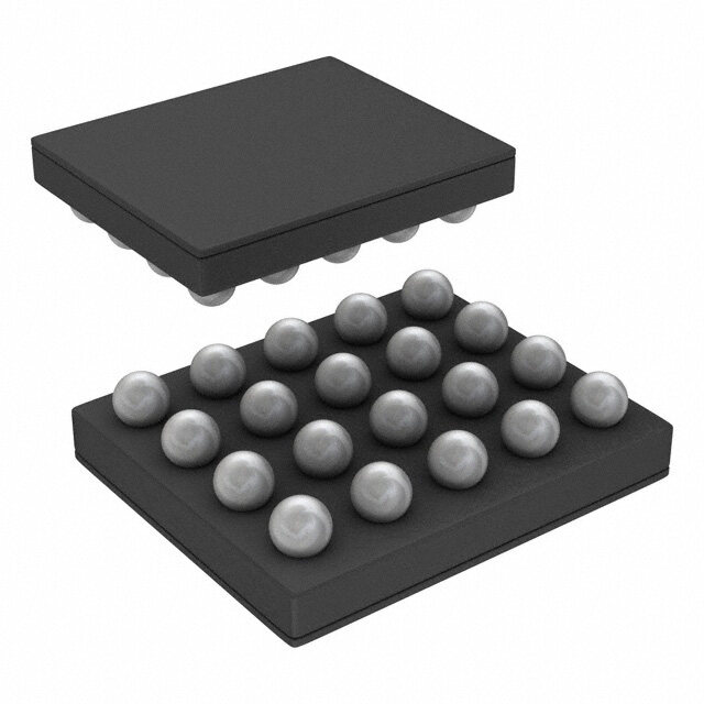
| 描述 | IC ANALOG FRONT END 16BIT 16DIP电信线路管理 IC 16 Bit Analog Proces |
| 产品分类 | 数据采集 - 模拟前端 (AFE)集成电路 - IC |
| 品牌 | Microchip Technology |
| 产品手册 | |
| 产品图片 |
|
| rohs | 符合RoHS无铅 / 符合限制有害物质指令(RoHS)规范要求 |
| 产品系列 | 通信及网络 IC,电信线路管理 IC,Microchip Technology TC500CPE- |
| 数据手册 | http://www.microchip.com/mymicrochip/filehandler.aspx?ddocname=en011527 |
| 产品型号 | TC500CPE |
| 产品 | Analog Front End |
| 产品目录页面 | |
| 产品种类 | 电信线路管理 IC |
| 位数 | 16 |
| 供应商器件封装 | 16-PDIP |
| 其它名称 | 158-1021 |
| 功率(W) | 10mW |
| 包装 | 管件 |
| 商标 | Microchip Technology |
| 安装风格 | Through Hole |
| 封装 | Tube |
| 封装/外壳 | 16-DIP(0.300",7.62mm) |
| 封装/箱体 | PDIP-16 |
| 工厂包装数量 | 30 |
| 接口类型 | Serial (3-Wire) |
| 最大工作温度 | + 70 C |
| 最小工作温度 | 0 C |
| 标准包装 | 30 |
| 电压-电源,数字 | 4.5 V ~ 7.5 V |
| 电压-电源,模拟 | 5V |
| 电源电压-最大 | +/- 7.5 V |
| 电源电压-最小 | +/- 4.5 V |
| 电源电流 | 1 mA |
| 类型 | Precision Analog Front Ends |
| 通道数 | 1 |
| 通道数量 | 1 Channel |


- 商务部:美国ITC正式对集成电路等产品启动337调查
- 曝三星4nm工艺存在良率问题 高通将骁龙8 Gen1或转产台积电
- 太阳诱电将投资9.5亿元在常州建新厂生产MLCC 预计2023年完工
- 英特尔发布欧洲新工厂建设计划 深化IDM 2.0 战略
- 台积电先进制程称霸业界 有大客户加持明年业绩稳了
- 达到5530亿美元!SIA预计今年全球半导体销售额将创下新高
- 英特尔拟将自动驾驶子公司Mobileye上市 估值或超500亿美元
- 三星加码芯片和SET,合并消费电子和移动部门,撤换高东真等 CEO
- 三星电子宣布重大人事变动 还合并消费电子和移动部门
- 海关总署:前11个月进口集成电路产品价值2.52万亿元 增长14.8%


PDF Datasheet 数据手册内容提取
TC500/A/510/514 Precision Analog Front Ends Features General Description • Precision (up to 17 bits) A/D Converter “Front TheTC500/A/510/514 family are precision analog front End” ends that implement dual slope A/D converters having (cid:127) 3-Pin Control Interface to Microprocessor a maximum resolution of 17 bits plus sign. As a minimum, each device contains the integrator, zero (cid:127) Flexible: User Can Trade-off Conversion Speed crossing comparator and processor interface logic. The for Resolution TC500 is the base (16-bit max) device and requires (cid:127) Single-Supply Operation (TC510/TC514) both positive and negative power supplies. The (cid:127) 4 Input, Differential Analog MUX (TC514) TC500A is identical to the TC500 with the exception (cid:127) Automatic Input Voltage Polarity Detection that it has improved linearity, allowing it to operate to a (cid:127) Low Power Dissipation: maximum resolution of 17 bits. The TC510 adds an on- - (TC500/TC500A): 10mW board negative power supply converter for single- supply operation. The TC514 adds both a negative - (TC510/TC514): 18mW power supply converter and a 4-input differential (cid:127) Wide Analog Input Range: analog multiplexer. - ±4.2V (TC500A/TC510) Each device has the same processor control interface (cid:127) Directly Accepts Bipolar and Differential consisting of 3 wires: control inputs (A and B) and zero- Input Signals crossing comparator output (CMPTR). The processor manipulates A, B to sequence the TC5XX through four Applications phases of conversion: auto-zero, integrate, de-inte- grate and integrator zero. During the auto-zero phase, (cid:127) Precision Analog Signal Processor offset voltages in the TC5XX are corrected by a closed (cid:127) Precision Sensor Interface loop feedback mechanism. The input voltage is applied (cid:127) High Accuracy DC Measurements to the integrator during the integrate phase. This causes an integrator output dv/dt directly proportional to the magnitude of the input voltage. The higher the input voltage, the greater the magnitude of the voltage stored on the integrator during this phase. At the start of the de-integrate phase, an external voltage reference is applied to the integrator and, at the same time, the external host processor starts its on-board timer. The processor maintains this state until a transition occurs on the CMPTR output, at which time the processor halts its timer. The resulting timer count is the converted analog data. Integrator zero (the final phase of conversion) removes any residue remaining in the integrator in preparation for the next conversion. The TC500/A/510/514 offer high resolution (up to 17 bits), superior 50/60Hz noise rejection, low-power operation, minimum I/O connections, low input bias currents and lower cost compared to other converter technologies having similar conversion speeds. 2004 Microchip Technology Inc. DS21428C-page 1
TC500/A/510/514 Package Types 16-Pin PDIP/SOIC/CERDIP 28-Pin PDIP/SOIC CINT 1 16 VDD VOUT– 1 28 CAP– VSS 2 15 DGND CINT 2 27 DGND CAZ 3 14 CMPTR OUT CAZ 3 26 CAP+ BUF 4 TC500/ 13 B BUF 4 25 VDD TC500A ACOM 5 12 A ACOM 5 24 OSC CREF– 6 11 VIN+ CREF– 6 23 CMPTR OUT CREF+ 7 10 VIN– CREF+ 7 22 A TC514 VREF− 8 9 VREF+ VREF– 8 21 B VREF+ 9 20 A0 24-Pin PDIP/SOIC CH4– 10 19 A1 VOUT– 1 24 CAP– CH3– 11 18 CH1+ CINT 2 23 DGND CH2– 12 17 CH2+ CAZ 3 22 CAP+ CH1– 13 16 CH3+ BUF 4 21 VDD N/C 14 15 CH4+ ACOM 5 20 OSC CREF– 6 19 CMPTR OUT TC510 CREF+ 7 18 A VREF– 8 17 B VREF+ 9 16 VIN+ N/C 10 15 VIN– N/C 11 14 N/C N/C 12 13 N/C Typical Application Control Logic CREF RINT CINT A0 B0 ZCeornov Ienrtteegr rSaatoter Output 0 1 Auto-Zero A0 A1 CREF+ VREF+ VREF- CREF- BCUAFZ CAZ CINT 11 01 DSieg-ninatle Ignrtaetgerate CH1+ SWR SWR Buffer Integrator TTCC550000A CCHH23++ MDUIFX. SWI -+ C+MPTR 1 CMPTR 2TTCC551104 CCHH41+- (TC514) SWRI- SWRI- + + LSehvieftl COMutPpuTtR CH2- CCHH34-- SWZ SWIZSWZ ACOM SWRI+ SWRI- DPeotelacrtiitoyn SWI SW1 Analog Phase Switch Decoding DGND Control Logic VSS DCCo-nTvOe-rDteCr Signals OSC (TC510 & TC514) VOUT- CAP- CAP+ 1.0µF VSS A B COUT- 1.0µF (TC500 Control Logic TC500A) DS21428C-page 2 2004 Microchip Technology Inc.
TC500/A/510/514 1.0 ELECTRICAL † Stresses above those listed under “Absolute Maxi- CHARACTERISTICS mum Ratings” may cause permanent damage to the device. These are stress ratings only and functional operation of the device at these or any other conditions Absolute Maximum Ratings† above those indicated in the operation sections of the specifications is not implied. Exposure to Absolute TC510/TC514 Positive Supply Voltage Maximum Rating conditions for extended periods may (V to GND).........................................+10.5V DD affect device reliability. TC500/TC500A Supply Voltage (V to V )..............................................+18V DD SS TC500/TC500A Positive Supply Voltage (V to GND)............................................+12V DD TC500/TC500A Negative Supply Voltage (V to GND)................................................-8V SS Analog Input Voltage (V + or V -)............V to V IN IN DD SS Logic Input Voltage...............V +0.3V to GND - 0.3V DD Voltage on OSC: ........................... -0.3V to (V +0.3V) for V < 5.5V DD DD Ambient Operating Temperature Range: ................................................................0°C to +70°C Storage Temperature Range:.............-65°C to +150°C DC CHARACTERISTICS Electrical Specifications: Unless otherwise specified, TC510/TC514: V = +5V, TC500/TC500A: V = ±5V. DD SS C = C = 0.47µF. AZ REF T = +25°C T = 0°C to 70°C A A Parameters Sym Units Conditions Min. Typ. Max. Min. Typ. Max. Analog Resolution 60 — — — — — µV Note1 Zero-scale Error with ZSE — — 0.005 — 0.005 0.012 % F.S. TC500/TC510/TC514 Auto-zero Phase — — 0.003 — 0.003 0.009 TC500A End Point Linearity ENL — 0.005 0.015 — 0.015 0.060 % F.S. TC500/TC510/TC514 — — 0.010 — 0.010 0.045 % F.S. Note1, Note2, TC500A Best-Case Straight NL — 0.003 0.008 — — — % F.S. TC500/TC510/TC514, Line Linearity Note1, Note2 — — 0.005 — — — % F.S. TC500A Zero-scale Temp. ZS — — — — 1 2 µV/°C Over Operating TC Coefficient Temperature Range Full-scale Symmetry SYE — 0.01 — — 0.03 — % F.S. Note1 Error (Rollover Error) Full-scale FS — — — — 10 — ppm/°C Over Operating TC Temperature Temperature Range; Coefficient External Reference TC = 0 ppm/°C Input Current I — 6 — — — — pA V = 0V IN IN Common Mode V V + 1.5 — V – 1.5 V + 1.5 — V – 1.5 V CMR SS DD SS DD Voltage Range Integrator Output V + 0.9 — V – 0.9 V + 0.9 — V + 0.9 V SS DD SS SS Swing Analog Input Signal V + 1.5 — V – 1.5 V + 1.5 — V + 1.5 V ACOM = GND = 0V SS DD SS SS Range Note 1: Integrate time ≥ 66msec, auto-zero time ≥ 66msec, V (peak) ≈ 4V. INT 2: End point linearity at ±1/4, ±1/2, ±3/4 F.S. after full-scale adjustment. 3: Rollover error is related to C , C , C characteristics. INT REF AZ 2004 Microchip Technology Inc. DS21428C-page 3
TC500/A/510/514 DC CHARACTERISTICS (CONTINUED) Electrical Specifications: Unless otherwise specified, TC510/TC514: V = +5V, TC500/TC500A: V = ±5V. DD SS C = C = 0.47µF. AZ REF T = +25°C T = 0°C to 70°C A A Parameters Sym Units Conditions Min. Typ. Max. Min. Typ. Max. Voltage Reference V V +1 — V – 1 V +1 — V – 1 V V - V + REF SS DD SS DD REF REF Range Digital Comparator Logic 1, V 4 — — 4 — — V I = 400µA OH SOURCE Output High Comparator Logic 0, V — — 0.4 — — 0.4 V I = 2.1mA OL SINK Output Low Logic 1, Input High V 3.5 — — 3.5 — — V IH Voltage Logic 0, Input Low V — — 1 — — 1 V IL Voltage Logic Input Current I — — — — 0.3 µA Logic ‘1’ or ‘0’ L Comparator Delay t — 2 — — 3 — µsec D Multiplexer (TC514 Only) Maximum Input -2.5 — 2.5 -2.5 — 2.5 V V = 5V DD Voltage Drain/Source ON R — 6 10 — — — kΩ V = 5V DSON DD Resistance Power (TC510/TC514 Only) Supply Current I — 1.8 2.4 — — 3.5 mA V = 5V, A = 1, B = 1 S DD Power Dissipation P — 18 — — — — mW V = 5V D DD Positive Supply V 4.5 — 5.5 4.5 — 5.5 V DD Operating Voltage Range Operating Source R — 60 85 — — 100 Ω I = 10mA OUT OUT Resistance Oscillator Frequency — 100 — — — — kHz Note1 Maximum Current Out I — — -10 — — -10 mA V = 5V OUT DD Power (TC500/TC500A Only) Supply Current I — 1 1.5 — — 2.5 mA V = ±5V, A = B = 1 S S Power Dissipation P — 10 — — — — mW V = 5V, V = -5V D DD SS Positive Supply V 4.5 — 7.5 4.5 — 7.5 V DD Operating Range Negative Supply V -4.5 — -7.5 - 4.5 — -7.5 V SS Operating Range Note 1: Integrate time ≥ 66msec, auto-zero time ≥ 66msec, V (peak) ≈ 4V. INT 2: End point linearity at ±1/4, ±1/2, ±3/4 F.S. after full-scale adjustment. 3: Rollover error is related to C , C , C characteristics. INT REF AZ DS21428C-page 4 2004 Microchip Technology Inc.
TC500/A/510/514 2.0 TYPICAL PERFORMANCE CURVES Note: The graphs and tables provided following this note are a statistical summary based on a limited number of samples and are provided for informational purposes only. The performance characteristics listed herein are not tested or guaranteed. In some graphs or tables, the data presented may be outside the specified operating range (e.g., outside specified power supply range) and therefore outside the warranted range. 5 -0 4 TVA+ == +52V5°C -1 TA = +25°C 3 Output Voltage (V)---321012 Slope 60Ω Output Voltage (V)-----56324 -7 -4 -5 -8 0 10 20 30 40 50 60 70 80 0 2 4 6 8 10 12 14 16 18 20 Load Current (mA) Output Current (mA) FIGURE 2-1: Output Voltage vs. Load FIGURE 2-4: Output Voltage vs. Output Current. Current. 200 100 mV PK-PK) 111257505 VO+s c=. F5rVe,q T. A= =1 0+02 5kC°HACzP = 1 µF Ωsistance () 8900 VIO+U =T 5=V 10 mA ple ( 100 e Re 70 p c Ri 75 CAP = 10 µF ur 60 ut So Outp 2550 utput 50 O 0 40 0 1 2 3 4 5 6 7 8 9 10 -50 -25 0 25 50 75 100 Load Current (mA) Temperature (°C) FIGURE 2-2: Output Ripple vs. Load FIGURE 2-5: Output Source Resistance Current. vs. Temperature. 100 150 V+ = 5V TA = +25°C Hz) V+ = 5V Hz) ncy (k ncy (k 125 e e qu 10 qu 100 e e Fr Fr or or Oscillat Oscillat 75 1 50 1 10 100 1000 -50 -25 0 25 50 75 100 125 Oscillator Capacitance (pF) Temperature (°C) FIGURE 2-3: Oscillator Frequency vs. FIGURE 2-6: Oscillator Frequency vs. Capacitance. Temperature. 2004 Microchip Technology Inc. DS21428C-page 5
TC500/A/510/514 3.0 PIN DESCRIPTIONS The descriptions of the pins are listed in Table3-1. TABLE 3-1: PIN FUNCTION TABLE Pin No. TC500, TC500A TC510 TC514 Symbol Function 1 2 2 C Integrator output. Integrator capacitor connection. INT 2 Not Used Not Used V Negative power supply input (TC500/TC500A only). SS 3 3 3 C Auto-zero input. The auto-zero capacitor connection. AZ 4 4 4 BUF Buffer output. The Integrator capacitor connection. 5 5 5 ACOM This pin is grounded in most applications. It is recommended that ACOM and the input common pin (Ve - orCH -) be within the analog Common Mode Range (CMR). n n 6 6 6 C - Input. Negative reference capacitor connection. REF 7 7 7 C + Input. Positive reference capacitor connection. REF 8 8 8 V - Input. External voltage reference (-) connection. REF 9 9 9 V + Input. External voltage reference (+) connection. REF 10 15 Not Used V - Negative analog input. IN 11 16 Not Used V + Positive analog input. IN 12 18 22 A Input. Converter phase control MSB. (See input B.) 13 17 21 B Input. Converter phase control LSB. The states of A, B place the TC5XX in one of four required phases. A conversion is complete when all four phases have been executed: Phase control input pins: AB = 00: Integrator zero 01: Auto-zero 10: Integrate 11: De-integrate 14 19 23 CMPTR Zero crossing comparator output. CMPTR is high during the integration phase when OUT a positive input voltage is being integrated and is low when a negative input voltage is being integrated. A high-to-low transition on CMPTR signals the processor that the De-integrate phase is completed. CMPTR is undefined during the auto-zero phase. It should be monitored to time the integrator zero phase. 15 23 27 DGND Input. Digital ground. 16 21 25 V Input. Power supply positive connection. DD — 22 26 CAP+ Input. Negative power supply converter capacitor (+) connection. — 24 28 CAP- Input. Negative power supply converter capacitor (-) connection. — 1 1 V - Output. Negative power supply converter output and reservoir capacitor connection. OUT This output can be used to power other devices in the circuit requiring a negative bias voltage. — 20 24 OSC Oscillator control input. The negative power supply converter normally runs at a frequency of 100kHz. The converter oscillator frequency can be slowed down (to reduce quiescent current) by connecting an external capacitor between this pin and V (see Section2.0 “Typical Performance Curves”). DD — — 18 CH1+ Positive analog input pin. MUX channel 1. — — 13 CH1- Negative analog input pin. MUX channel 1. — — 17 CH2+ Positive analog input pin. MUX channel 2. — — 12 CH2- Negative analog input pin. MUX channel 2. — — 16 CH3+ Positive analog input pin. MUX channel 3. — — 11 CH3- Negative analog input pin. MUX channel 3. — — 15 CH4+ Positive analog input pin. MUX channel 4. — — 10 CH4- Negative analog input pin. MUX channel 4 — — 20 A0 Multiplexer input channel select input LSB (see A1). — — 19 A1 Multiplexer input channel select input MSB. Phase control input pins: A1, A0 = 00 = Channel 1 01 = Channel 2 10 = Channel 3 11 = Channel 4 DS21428C-page 6 2004 Microchip Technology Inc.
TC500/A/510/514 4.0 DETAILED DESCRIPTION multiples of the integration period are, theoretically, completely removed, since the average value of a sine wave of frequency (1/T) averaged over a period (T) is 4.1 Dual Slope Conversion Principles zero. Actual data conversion is accomplished in two phases: Integrating converters often establish the integration input signal integration and reference voltage de- period to reject 50/60 Hz line frequency interference integration. signals. The ability to reject such signals is shown by a The integrator output is initialized to 0V prior to the start normal mode rejection plot (Figure4-1). Normal mode of integration. During integration, analog switch S con- rejection is limited in practice to 50 to 65dB, since the 1 nects V to the integrator input where it is maintained line frequency can deviate by a few tenths of a percent IN for a fixed time period (T ). The application of V (Figure4-2). INT IN causes the integrator output to depart 0V at a rate deter- mined by the magnitude of V and a direction deter- 30 IN ) mined by the polarity of VIN. The de-integration phase is dB T = MPeeraiosdurment initiated immediately at the expiration of T . ( INT n o During de-integration, S1 connects a reference voltage cti20 (having a polarity opposite that of V ) to the integrator e IN ej input. At the same time, an external precision timer is R started. The de-integration phase is maintained until e d the comparator output changes state, indicating the o10 M integrator has returned to its starting point of 0V. When al this occurs, the precision timer is stopped. The de- m integration time period (T ), as measured by the or DEINT N 0 precision timer, is directly proportional to the magnitude 0.1/T 1/T 10/T of the applied input voltage (see Figure4-3). Input Frequency A simple mathematical equation relates the input FIGURE 4-1: Integrating Converter signal, reference voltage and integration time: Normal Mode Rejection. EQUATION 4-1: -----------1-------------∫TINTV (T)DT = V----R----E---F---C----D----E---I--N----T- 80 R C 0 IN R C B) INT INT INT INT d 70 ( Where: on t = 0.1 sec cit 60 VREF = Reference Voltage eje TINT = Signal Integration time (fixed) e R 50 t = Reference Voltage Integration time (variable) d DEINT o M 40 For a constant VIN: ormal 30 NRoErmJEaCl MTIoOdNe= 20 LOG SIN 6600 pp tt ((11 ±± DD 11 EE00 00 VV )) EQUATION 4-2: N Dt E= VIn =te Dgreavtiioantio Pne frrioomd 60 Hz 20 V = V T----D----E---I--N---T-- 0.01 0.1 1.0 IN REF T Line Frequency Deviation from 60 Hz (%) INT FIGURE 4-2: Line Frequency Deviation. The dual slope converter accuracy is unrelated to the integrating resistor and capacitor values as long as they are stable during a measurement cycle. An inherent benefit is noise immunity. Input noise spikes are integrated (averaged to zero) during the integration periods. Integrating ADCs are immune to the large conversion errors that plague successive approximation converters in high noise environments. Integrating converters provide inherent noise rejection with at least a 20dB/decade attenuation rate. Interference signals with frequencies at integral 2004 Microchip Technology Inc. DS21428C-page 7
TC500/A/510/514 C INT TC510 R Integrator Analog INT – V Input (VIN) INT – Comparator CMPTR Out + + S 1 ± Phase Switch Driver Ref Control Control Voltage Polarity Control Logic A B V I/O r SUPPLY ntegratoOutput VVIINN ≈≈ V1/R2E VFREF VINT ROMMicrocompTuitmeerr I RAM Counter T T INT DEINT FIGURE 4-3: Basic Dual Slope Converter. DS21428C-page 8 2004 Microchip Technology Inc.
TC500/A/510/514 5.0 TC500/A/510/514 CONVERTER The internal analog switch status for each of these OPERATION phases is summarized in Table5-1. This table references the Typical Application. The TC500/A/510/514 incorporates an auto-zero and Integrator phase in addition to the input signal Integrate and reference De-integrate phases. The addition of these phases reduce system errors, calibration steps and shorten overrange recovery time. A typical measurement cycle uses all four phases in the following order: 1. Auto-zero. 2. Input signal integration. 3. Reference de-integration. 4. Integrator output zero. TABLE 5-1: INTERNAL ANALOG GATE STATUS Conversion Phase SW SW + SW - SW SW SW SW I R R Z R 1 IZ Auto-zero (A = 0, B = 1) — — — Closed Closed Closed — Input Signal Integration (A = 1, B = 0) Closed — — — — — — Reference Voltage De-integration * (A =1, B = 1) — Closed — — — Closed — Integrator Output Zero (A = 0, B = 0) — — — — Closed Closed Closed *Assumes a positive polarity input signal. SW– would be closed for a negative input signal. RI 5.1 Auto-zero Phase (AZ) 5.3 Reference Voltage De-integration Phase (D ) During this phase, errors due to buffer, integrator and INT comparator offset voltages are nulled out by charging The previously charged reference capacitor is CAZ (auto-zero capacitor) with a compensating error connected with the proper polarity to ramp the voltage. integrator output back to zero. An externally-provided, The external input signal is disconnected from the precision timer is used to measure the duration of this internal circuitry by opening the two SW switches. The phase. The resulting time measurement is proportional I internal input points connect to analog common. The to the magnitude of the applied input voltage. reference capacitor is charged to the reference voltage potential through SW . A feedback loop, closed around 5.4 Integrator Output Zero Phase (IZ) R the integrator and comparator, charges the capacitor This phase ensures the integrator output is at 0V when (C ) with a voltage to compensate for buffer amplifier, AZ the auto-zero phase is entered, and that only system integrator and comparator offset voltages. offset voltages are compensated. This phase is used at the end of the reference voltage de-integration phase 5.2 Analog Input Signal Integration and MUST be used for ALL TC5XX applications having Phase (INT) resolutions of 12-bits or more. If this phase is not used, the value of the auto-zero capacitor (C ) must be The TC5XX integrates the differential voltage between AZ about 2 to 3 times the value of the integration capacitor the V + and V – inputs. The differential voltage must IN IN (C ) to reduce the effects of charge sharing. The inte- be within the device's Common mode range V . The INT CMR grator output zero phase should be programmed to input signal polarity is normally checked via software at operate until the output of the comparator returns high. the end of this phase: CMPTR = 1 for positive polarity; The overall timing system is shown in Figure5-1. CMPTR = 0 for negative polarity. 2004 Microchip Technology Inc. DS21428C-page 9
TC500/A/510/514 TTIME Converter Status Auto-zero Integrate Reference Overshoot Integrator Full-scale Input De-integrate Output Zero Integrator 0 Voltage VINT Comparator Delay Comparator Undefined 0 For Negative Input Output 1 For Positive Input A A = 0 A = 1 A = 1 A = 0 AB Inputs B = 1 B = 0 B = 1 B = 0 B Controller Begin Conversion with Time Input Capture Integrator Ready for Next Operation Auto-Zero Phase Integration De-integration Output Conversion Phase Time Zero Phase (Auto-Zero is Complete Idle State) Sample Input Polarity Typically = TINT TINT Minimizing Overshoot (Positive Input Shown) Comparator Delay + will Minimize Processor Latency I.O.Z. Time Notes: The length of this phase is chosen almost arbitrarily but needs to be long enough to null out worst case errors (see text). FIGURE 5-1: Typical Dual Slope A/D Converter System Timing. DS21428C-page 10 2004 Microchip Technology Inc.
TC500/A/510/514 6.0 ANALOG SECTION The difference in reference for (+) or (-) input voltages will cause a rollover error. This error can be minimized by using a large reference capacitor in comparison to 6.1 Differential Inputs (V +, V –) IN IN the stray capacitance. The TC5XX operates with differential voltages within the input amplifier Common mode range. The amplifier 6.4 Phase Control Inputs (A, B) Common mode range extends from 1.5V below positive supply to 1.5V above negative supply. Within The A, B unlatched logic inputs select the TC5XX this Common mode voltage range, Common mode operating phase. The A,B inputs are normally driven rejection is typically 80dB. Full accuracy is maintained, by a microprocessor I/O port or external logic. however, when the inputs are no less than 1.5V from either supply. 6.5 Comparator Output The integrator output also follows the Common mode By monitoring the comparator output during the fixed voltage. The integrator output must not be allowed to signal integrate time, the input signal polarity can be saturate. A worst-case condition exists, for example, determined by the microprocessor controlling the when a large, positive Common mode voltage, with a conversion. The comparator output is high for positive near full-scale negative differential input voltage, is signals and low fornegative signals during the signal applied. The negative input signal drives the integrator integrate phase (see Figure6-1). positive when most of its swing has been used up by During the reference de-integrate phase, the the positive Common mode voltage. For these critical comparator output will make a high-to-low transition as applications, the integrator swing can be reduced. The the integrator output ramp crosses zero. The transition integrator output can swing within 0.9V of either supply is used to signal the processor that the conversion is without loss of linearity. complete. 6.2 Analog Common The internal comparator delay is 2µsec, typically. Figure6-1 shows the comparator output for large Analog common is used as VIN return during system positive and negative signal inputs. For signal inputs at zero and reference de-integrate. If VIN– is different from or near zero volts, however, the integrator swing is very analog common, a Common mode voltage exists in the small. If Common mode noise is present, the system. This signal is rejected by the excellent CMR of comparator can switch several times during the the converter. In most applications, VIN– will be set at a beginning of the signal integrate period. To ensure that fixed known voltage (i.e., power supply common). A the polarity reading is correct, the comparator output Common mode voltage will exist when VIN– is not should be read and stored at the end of the signal connected to analog common. integrate phase. The comparator output is undefined during the auto- 6.3 Differential Reference zero phase and is used to time the integrator output (VREF+, VREF–) zero phase. (See Section8.6 “Integrator Output Zero Phase”). The reference voltage can be anywhere within 1V of the power supply voltage of the converter. Rollover error is caused by the reference capacitor losing or gaining charge due to stray capacitance on its nodes. Signal Reference Signal Reference Integrate Deintegrate Integrate De-integrate Integrator Output Zero Crossing Integrator Output Zero Crossing Comparator Comparator Output Output A. Positive Input Signal B. Negative Input Signal FIGURE 6-1: Comparator Output. 2004 Microchip Technology Inc. DS21428C-page 11
TC500/A/510/514 7.0 TYPICAL APPLICATIONS TABLE 7-1: C AND C SELECTION REF AZ Conversions Typical Value of Suggested* Part 7.1 Component Value Selection Per Second C , C (µF) Number REF AZ The procedure outlined below allows the user to arrive >7 0.1 SMR5 104K50J01L4 at values for the following TC5XX design variables: 2 to 7 0.22 SMR5 224K50J02L4 1. Integration Phase Timing. 2 or less 0.47 SMR5 474K50J04L4 2. Integrator Timing Components (R , C ). * Manufactured by Evox Rifa, Inc. INT INT 3. Auto-zero and Reference Capacitors. 7.6 Calculate Integrating Capacitor 4. Voltage Reference. (C ) INT 7.2 Select Integration Time The integrating capacitor must be selected to maximize integrator output voltage swing. The integrator output Integration time must be picked as a multiple of the voltage swing is defined as the absolute value of V period of the line frequency. For example, T times of DD INT (or V ) less 0.9V (i.e., IV - 0.9VI or IV + 0.9VI). 33msec, 66msec and 132msec maximize 60Hz line SS DD SS Using the 20µA buffer maximum output current, the rejection. value of the integrating capacitor is calculated using the following equation. 7.3 DINT and IZ Phase Timing The duration of the DINT phase is a function of the EQUATION 7-2: amount of voltage stored on the integrator during TINT (T )(20×10–6) and the value of VREF. The DINT phase must be initiated CINT = -------I-N---(-T-V--------–----0---.--9---)------------ immediately following INT and terminated when an inte- S grator output zero-crossing is detected. In general, the Where: maximum number of counts chosen for DINT is twice T = Integration Period that of INT (with V chosen at V /2). INT REF IN(MAX) V = IV I or IV I, whichever is less (TC500/A) S DD SS 7.4 Calculate Integrating Resistor V = IV I (TC510, TC514) S DD (R ) INT It is critical that the integrating capacitor has a very low The desired full-scale input voltage and amplifier output dielectric absorption. Polypropylene capacitors are an current capability determine the value of R . The INT example of one such dialectic. Polyester and poly- buffer and integrator amplifiers each have a full-scale bicarbonate capacitors may also be used in less critical current of 20µA. applications. Table7-2 summarizes recommended The value of RINT is, therefore, directly calculated in the capacitors for CINT. following equation: TABLE 7-2: RECOMMENDED CAPACITOR EQUATION 7-1: FOR CINT R (in MΩ) = V----I--N----(--M----A---X----) Value Suggested INT 20 Part Number* Where: 0.1 SMR5 104K50J01L4 V = Maximum input voltage (full count voltage) 0.22 SMR5 224K50J02L4 IN(MAX) R = Integrating Resistor (in MΩ) 0.33 SMR5 334K50J03L4 INT For loop stability, R should be ≥ 50kΩ. 0.47 SMR5 474K50J04L4 INT *Manufactured by Evox-Rifa, Inc. 7.5 Select Reference (C ) and Auto- REF 7.7 Calculate V zero (C ) Capacitors REF AZ The reference de-integration voltage is calculated C and C must be low leakage capacitors (such as REF AZ using the following equation: polypropylene). The slower the conversion rate, the larger the value C must be. Recommended REF EQUATION 7-3: capacitors for C and C are shown in Table7-1. REF AZ Larger values for C and C may also be used to (V –0.9)(C )(R ) limit rollover errors.AZ REF VREF = -------S-------------2---(---R------I--N----T)-----------I--N----T----V INT DS21428C-page 12 2004 Microchip Technology Inc.
TC500/A/510/514 8.0 DESIGN CONSIDERATIONS 8.4 Input Signal Integrate Phase The length of this phase is constant from one 8.1 Noise conversion to the next and depends on system parameters and component value selections. The The threshold noise (N ) is the algebraic sum of the TH calculation of T is shown elsewhere in this data integrator and comparator noise and is typically 30µV. INT sheet. At some point near the end of this phase, the Figure8-1 illustrates how the value of the reference microcontroller should sample CMPTR to determine voltage can affect the final count. Such errors can be the input signal polarity. This value is, in effect, the Sign reduced by increased integration times, in the same Bit for the overall conversion result. Optimally, CMPTR way that 50/60Hz noise is rejected. The signal-to- should be sampled just before this phase is terminated noise ratio is related to the integration time (T ) and INT by changing AB from 10 to 11. The consideration here the integration time constant (R , C ) as follows: INT INT is that, during the initial stage of input integration when EQUATION 8-1: the integrator voltage is low, the comparator may be affected by noise and its output unreliable. Once V t S/N (dB) = 20 log------------I--N---------•-----------------I--N----T---------------- integration is well underway, the comparator will be in a 30×10–6 (RINT)•(CINT) defined state. 8.5 Reference De-integration 8.2 System Timing The length of this phase must be precisely measured To obtain maximum performance from the TC5XX, the from the transition of AB from 10 to 11 to the falling- overshoot at the end of the de-integration phase must edge of CMPTR. The comparator delay contributes be minimized. Also, the integrator output zero phase some error in timing this phase. The typical delay is must be terminated as soon as the comparator output specified to be 2µsec. This should be considered in the returns high (see Figure5-1). context of the length of a single count when Figure5-1 shows the overall timing for a typical system determining overall system performance and possible in which a TC5XX is interfaced to a microcontroller. The single count errors. Additionally, overshoot will result in microcontroller drives the A, B inputs with I/O lines and charge accumulating on the integrator once its output monitors the comparator output (CMPTR) using an I/O crosses zero. This charge must be nulled during the line or dedicated timer capture control pin. It may be integrator output zero phase. necessary to monitor the state of the CMPTR output in addition to having it control a timer directly for the Reference de-integration phase (this is further explained below.) The timing diagram in Figure5-1 is not to scale, as the timing in a real system depends on many system parameters and component value selections. There are four critical timing events (as shown in Figure5-1): sampling the input polarity, capturing the de-integration time, minimizing overshoot and properly executing the integrator output zero phase. 8.3 Auto-zero Phase The length of this phase is usually set to be equal to the input signal integration time. This decision is virtually arbitrary since the magnitudes of the various system errors are not known. Setting the auto-zero time equal to the Input Integrate time should be more than adequate to null out system errors. The system may remain in this phase indefinitely (i.e., auto-zero is the appropriate Idle state for a TC5XX device). 2004 Microchip Technology Inc. DS21428C-page 13
TC500/A/510/514 S S S 30V NTH NTH NTH Low VREF Normal VREF High VREF V REF Slope (S) = N = Noise Threshold R C TH INT INT FIGURE 8-1: Noise Threshold. 8.6 Integrator Output Zero Phase 8.7 Using the TC510/TC514 The comparator delay and the controller's response 8.7.1 NEGATIVE SUPPLY VOLTAGE latency may result in overshoot, causing charge CONVERTER (TC510, TC514) buildup on the integrator at the end of a conversion. This charge must be removed or performance will A capacitive charge pump is employed to invert the degrade. The integrator output zero phase should be voltage on VDD for negative bias within the TC510/ activated (AB = 00) until CMPTR goes high. It is TC514. This voltage is also available on the VOUT- pin absolutely critical that this phase be terminated to provide negative bias elsewhere in the system. Two immediately so that overshoot is not allowed to occur in external capacitors are required to perform the the opposite direction. At this point, it can be assured conversion. that the integrator is near zero. Auto-zero should be Timing is generated by an internal state machine driven entered (AB = 01) and the TC5XX held in this state until from an on-board oscillator. During the first phase, the next cycle is begun (see Figure8-2). capacitor C is switched across the power supply and F charged to V +. This charge is transferred to capacitor S C - during the second phase. The oscillator normally OUT Integrator Zero runs at 100kHz to ensure minimum output ripple. This Output Crossing frequency can be reduced by placing a capacitor from OSC to V . The relationship between the capacitor DD value is shown in Section2.0 “Typical Performance Curves”. Overshoot 8.7.2 ANALOG INPUT MULTIPLEXER (TC514) Comparator The TC514 is equipped with a four-input differential Output Comp analog multiplexer. Input channels are selected using De-integrate Phase select inputs (A1, A0). These are high-true control Integrate Integrator signals (i.e., channel 0 is selected when (A1, A0 = 00). Phase Zero Phase FIGURE 8-2: Overshoot. DS21428C-page 14 2004 Microchip Technology Inc.
TC500/A/510/514 9.0 DESIGN EXAMPLES Refer to Figures 9-1 to 9-4. Given: Required Resolution: 16 bits (65,536 counts). Maximum V : ±2V IN Power Supply Voltage: +5V 60Hz System Step 1. Pick integration time (t ) as a multiple INT of the line frequency: 1/60Hz = 16.6msec. Use 4x line frequency. = 66msec Step 2. Calculate R : INT R = V /20µA 2 /20µA INT IN(MAX) = 100kΩ Step 3. Calculate C for maximum (4V) INT integrator output swing. C = (t ) (20 x 10 –6) / (V - 0.9) INT INT S = (.066) (20 x 10 –6) / (4.1) = 0.32µF (use closest value: 0.33µF) Note: Microchip recommended capacitor: Evox-Rifa p/n: 5MR5 334K50J03L4. Step 4. Choose C and C based on REF AZ conversion rate. Conversions/sec: = 1/(T + T + 2 T + 2msec) AZ INT INT = 1/(66msec +66msec +132msec +2msec) = 3.7 conversions/sec From which C = C = 0.22µF AZ REF (see Table7-1) Note: Microchip recommended capacitor: Evox-Rifa p/n: 5MR5 224K50J02L4 Step 5. Calculate V : REF EQUATION 9-1: (V –0.9)(C )(R ) V = -------S-------------------------I--N----T-----------I--N----T---- REF 2(T ) INT = (4.1)(0.33×1–6)(105) -------------------------------------------------------------- 2(0.66) = 1.025 2004 Microchip Technology Inc. DS21428C-page 15
TC500/A/510/514 1 24 1µF 0.C33INTµF 2 VOUT- CAP- 23 Typical Waveforms CINT DGND 1µF +5V CAZ 0.22µF3 CAZ TC510 CAP+ 22 Pin 2 +5V 4 BUF VDD 21 +5V VIN+ 10R0INkTΩ 5 PICmicro® Pin 19 ACOM Microcontroller MCP1525 CREF 6 CREF- CMPTR 19 1R02kΩ0.22µF 7 CREF+ A 18 VIN-Pin 2 1µF R3, 10kΩ 9 VREF+ B 17 Pin 19 0.01CµF1 8 VREF- VIN+ 16 INPUT+ VIN- 15 INPUT- FIGURE 9-1: TC510 Design Sample. 1 28 VOUT- CAP- 1µF CINT 0.33µF 2 27 CINT DGND 1µF +5V CAZ 0.22µF 26 3 CAZ CAP+ 25 +5V RINT 4 BUF TC514 VDD 22 +5V 100kΩ 5 A0 Analog PICmicro® ACOM A1 19 Mux Logic Microcontroller MCP1525 CREF 6 CREF- CMPTR 23 1R02k0Ω.22µF 7 CREF+ A 22 1µF R3, 10kΩ 9 VREF+ B 21 0.01CµF1 8 VREF- CH1+ 18 INPUT 1+ 13 CH1- INPUT 1- Typical Waveforms CH2+ 17 INPUT 2+ PIN 2 CH2- 12 INPUT 2- VIN+ CH3+ 16 INPUT 3+ CH3- 11 INPUT 3- PIN 23 CH4+ 15 INPUT4+ PIN 2 CH4- 10 INPUT4- VIN- PIN 23 FIGURE 9-2: TC514 Design Example. DS21428C-page 16 2004 Microchip Technology Inc.
TC500/A/510/514 +5V 21 1 1µF VDD VOUT- 24 CAP- 1µF CAP+ 22 7 C + REF 0.22µF 10kΩ C - 6 REF MCP1525 9 V + REF TC510 10kΩ 1µF 0.01µF 8 V - REF PC 4 100kΩ Printer BUF Port 2 18 A C 3 0.22µF AZ PORT 17 0.33µF 0378 3 B CINT 2 HEX 10 19 16 100kΩ CMPTR VIN+ + 0.01µF V - 15 Input IN – 5 ACOM DGND 23 FIGURE 9-3: TC510 To IBM® Compatible Printer Port. 2004 Microchip Technology Inc. DS21428C-page 17
TC500/A/510/514 +5V 25 1 18 28 1µF + CH1+ VDD VOUT CAP– Input 1 1µF – 13 CH1– 26 10kΩ CAP+ 17 + CH2+ Input 2 7 – 12 CH2– CREF+ MCP1525 16 0.22µF + CH3+ 6 Input 3 CREF- 10kΩ 11 – CH3– + 15 CH4+ VREF+ 9 10kΩ Input 4 10 CH4– TC514 0.01µF – 8 V - REF 20 A0 Analog Mux Control Logic 19 100kΩ IBM® A1 BUF 4 Printer Port 2 22 3 A C AZ Port 3 21 2 0.22µF 0.33µF 0378 B CINT Hex 10 23 CMPTR 5 ACOM DGND 27 FIGURE 9-4: TC514 To IBM® Compatible Printer Port. DS21428C-page 18 2004 Microchip Technology Inc.
TC500/A/510/514 10.0 PACKAGING INFORMATION 10.1 Package Marking Information 16-Lead CERDIP (300 mil) Example: XXXXXXXXXXXXXX TC500AIJE XXXXXXXXXXXXXX 0441256 YYWWNNN 16-Lead PDIP (300 mil) Example: XXXXXXXXXXXXXX TC500CPE XXXXXXXXXXXXXX 0441256 YYWWNNN 16-Lead SOIC (300 mil) Example: XXXXXXXXXXXXX TC500ACOE XXXXXXXXXXXXX 0441256 YYWWNNN Legend: XX...X Customer specific information* YY Year code (last 2 digits of calendar year) WW Week code (week of January 1 is week ‘01’) NNN Alphanumeric traceability code Note: In the event the full Microchip part number cannot be marked on one line, it will be carried over to the next line thus limiting the number of available characters for cus- tomer specific information. * Standard marking consists of Microchip part number, year code, week code, traceability code. For marking beyond this, certain price adders apply. Please check with your Microchip Sales Office. 2004 Microchip Technology Inc. DS21428C-page 19
TC500/A/510/514 Package Marking Information (Continued) 24-Lead PDIP (300 mil) Example: XXXXXXXXXXXXX TC510CPF YYWWNNN 0441256 24-Lead SOIC (300 mil) Example: XXXXXXXXXXXXX TC510COG XXXXXXXXXXXXX 0441256 YYWWNNN 28-Lead PDIP (300 mil) Example: XXXXXXXXXXXXXX TC514CPJ XXXXXXXXXXXXXX 0441256 YYWWNNN 28-Lead SOIC (300 mil) Example: XXXXXXXXXXXXX XXXXXXXXXXXXX TC514COI XXXXXXXXXXXXX 0441256 YYWWNNN DS21428C-page 20 2004 Microchip Technology Inc.
TC500/A/510/514 16-Lead Ceramic Dual In-line (JE) – 300 mil (CERDIP) E1 D 2 n 1 E A2 A L c A1 B1 eB B p Units INCHES* MILLIMETERS Dimension Limits MIN NOM MAX MIN NOM MAX Number of Pins n 18 18 Pitch p .100 2.54 Top to Seating Plane A .160 .180 .200 4.06 4.57 5.08 Standoff § A1 .015 .030 .040 0.38 0.76 1.02 Shoulder to Shoulder Width E .290 .305 .325 7.37 7.75 8.25 Ceramic Pkg. Width E1 .280 .288 .296 7.11 7.32 7.52 Overall Length D .752 .760 .780 19.10 19.30 19.81 Tip to Seating Plane L .125 .163 .200 3.18 4.14 5.08 Lead Thickness c .008 .012 .014 0.20 0.30 0.36 Upper Lead Width B1 .045 .055 .065 1.14 1.40 1.65 Lower Lead Width B .015 .018 .021 0.38 0.46 0.53 Overall Row Spacing eB .325 .360 .410 8.25 9.14 10.41 *Controlling Parameter JEDEC Equivalent: MS-030 Drawing No. C04-003 2004 Microchip Technology Inc. DS21428C-page 21
TC500/A/510/514 16-Lead Plastic Dual In-line (PE) – 300 mil (PDIP) E1 D 2 α n 1 E A A2 c L β A1 B1 eB B p Units INCHES* MILLIMETERS Dimension Limits MIN NOM MAX MIN NOM MAX Number of Pins n 16 16 Pitch p .100 2.54 Top to Seating Plane A .140 .155 .170 3.56 3.94 4.32 Molded Package Thickness A2 .115 .130 .145 2.92 3.30 3.68 Base to Seating Plane A1 .015 0.38 Shoulder to Shoulder Width E .300 .313 .325 7.62 7.94 8.26 Molded Package Width E1 .240 .250 .260 6.10 6.35 6.60 Overall Length D .740 .750 .760 18.80 19.05 19.30 Tip to Seating Plane L .125 .130 .135 3.18 3.30 3.43 Lead Thickness c .008 .012 .015 0.20 0.29 0.38 Upper Lead Width B1 .045 .058 .070 1.14 1.46 1.78 Lower Lead Width B .014 .018 .022 .036 0.46 0.56 Overall Row Spacing § eB .310 .370 .430 7.87 9.40 10.92 Mold Draft Angle Top α 5 10 15 5 10 15 Mold Draft Angle Bottom β 5 10 15 5 10 15 * Controlling Parameter § Significant Characteristic Notes: Dimensions D and E1 do not include mold flash or protrusions. Mold flash or protrusions shall not exceed .010” (0.254mm) per side. JEDEC Equivalent: MS-001 Drawing No. C04-017 DS21428C-page 22 2004 Microchip Technology Inc.
TC500/A/510/514 16-Lead Plastic Small Outline (OE) – Wide, 300 mil (SOIC) E p E1 D 2 n 1 B h α 45° c A A2 φ β L A1 Units INCHES* MILLIMETERS Dimension Limits MIN NOM MAX MIN NOM MAX Number of Pins n 16 16 Pitch p .050 1.27 Overall Height A .093 .099 .104 2.36 2.50 2.64 Molded Package Thickness A2 .088 .091 .094 2.24 2.31 2.39 Standoff § A1 .004 .008 .012 0.10 0.20 0.30 Overall Width E .394 .407 .420 10.01 10.34 10.67 Molded Package Width E1 .291 .295 .299 7.39 7.49 7.59 Overall Length D .398 .406 .413 10.10 10.30 10.49 Chamfer Distance h .010 .020 .029 0.25 0.50 0.74 Foot Length L .016 .033 .050 0.41 0.84 1.27 Foot Angle φ 0 4 8 0 4 8 Lead Thickness c .009 .011 .013 0.23 0.28 0.33 Lead Width B .014 .017 .020 0.36 0.42 0.51 Mold Draft Angle Top α 0 12 15 0 12 15 Mold Draft Angle Bottom β 0 12 15 0 12 15 * Controlling Parameter § Significant Characteristic Notes: Dimensions D and E1 do not include mold flash or protrusions. Mold flash or protrusions shall not exceed .010” (0.254mm) per side. JEDEC Equivalent: MS-013 Drawing No. C04-102 2004 Microchip Technology Inc. DS21428C-page 23
TC500/A/510/514 24-Lead Skinny Plastic Dual In-line (PF) – 300 mil (PDIP) E1 D 2 n 1 α E A A2 c L A1 β B1 p eB B Units INCHES* MILLIMETERS Dimension Limits MIN NOM MAX MIN NOM MAX Number of Pins n 24 24 Pitch p .100 2.54 Top to Seating Plane A .140 .150 .160 3.56 3.81 4.06 Molded Package Thickness A2 .115 .130 .145 2.92 3.30 3.68 Base to Seating Plane A1 .015 0.38 Shoulder to Shoulder Width E .295 .310 .325 7.49 7.87 8.26 Molded Package Width E1 .240 .250 .260 6.10 6.35 6.60 Overall Length D 1.245 1.250 1.255 31.62 31.75 31.88 Tip to Seating Plane L .120 .125 .130 3.05 3.18 3.30 Lead Thickness c .008 .012 .015 0.20 0.29 0.38 Upper Lead Width B1 .045 .053 .060 1.14 1.33 1.52 Lower Lead Width B .014 .018 .022 0.36 0.46 0.56 Overall Row Spacing § eB .310 .370 .430 7.87 9.40 10.92 Mold Draft Angle Top α 5 10 15 5 10 15 Mold Draft Angle Bottom β 5 10 15 5 10 15 * Controlling Parameter § Significant Characteristic Notes: Dimensions D and E1 do not include mold flash or protrusions. Mold flash or protrusions shall not exceed .010” (0.254mm) per side. JEDEC Equivalent: MO-001 Drawing No. C04-043 DS21428C-page 24 2004 Microchip Technology Inc.
TC500/A/510/514 24-Lead Plastic Small Outline (OG) – Wide, 300 mil (SOIC) E E1 e D B 2 n 1 a h h c A f L A1 A2 b Units INCHES MILLIMETERS* Dimension Limits MIN NOM MAX MIN NOM MAX Number of Pins n 24 24 Pitch e .050 BSC 1.27 BSC Overall Height A .093 -- .104 2.35 -- 2.65 Molded Package Thickness A2 .081 -- .100 2.05 -- 2.55 Standoff A1 .004 -- .012 0.10 -- 0.30 Overall Width E .406 BSC 10.30 BSC Molded Package Width E1 .295 BSC 7.50 BSC Overall Length D .607 BSC 15.40 BSC Chamfer Distance h .010 -- .030 0.25 -- 0.75 Foot Length L .016 -- .050 0.40 -- 1.27 Foot Angle Top f 0° -- 8° 0° -- 8° Lead Thickness c .008 -- .013 0.20 -- 0.33 Lead Width B .012 -- .020 0.31 -- 0.51 Mold Draft Angle Top a 5° -- 15° 5° -- 15° Mold Draft Angle Bottom b 5° -- 15° 5° -- 15° *Controlling Parameter per JEDEC MS-103 Revision C. Notes: Dimensions D and E1 do not include mold flash or protrusions. Mold flash or protrusions shall not exceed .010" (0.254mm) per side. JEDEC Equivalent: MS-013 AD Drawing No. C04-025 2004 Microchip Technology Inc. DS21428C-page 25
TC500/A/510/514 28-Lead Skinny Plastic Dual In-line (PJ) – 300 mil (PDIP) E1 D 2 n 1 α E A2 A L c β A1 B1 eB B p Units INCHES* MILLIMETERS Dimension Limits MIN NOM MAX MIN NOM MAX Number of Pins n 28 28 Pitch p .100 2.54 Top to Seating Plane A .140 .150 .160 3.56 3.81 4.06 Molded Package Thickness A2 .125 .130 .135 3.18 3.30 3.43 Base to Seating Plane A1 .015 0.38 Shoulder to Shoulder Width E .300 .310 .325 7.62 7.87 8.26 Molded Package Width E1 .275 .285 .295 6.99 7.24 7.49 Overall Length D 1.345 1.365 1.385 34.16 34.67 35.18 Tip to Seating Plane L .125 .130 .135 3.18 3.30 3.43 Lead Thickness c .008 .012 .015 0.20 0.29 0.38 Upper Lead Width B1 .040 .053 .065 1.02 1.33 1.65 Lower Lead Width B .016 .019 .022 0.41 0.48 0.56 Overall Row Spacing § eB .320 .350 .430 8.13 8.89 10.92 Mold Draft Angle Top α 5 10 15 5 10 15 Mold Draft Angle Bottom β 5 10 15 5 10 15 * Controlling Parameter § Significant Characteristic Notes: Dimension D and E1 do not include mold flash or protrusions. Mold flash or protrusions shall not exceed .010” (0.254mm) per side. JEDEC Equivalent: MO-095 Drawing No. C04-070 DS21428C-page 26 2004 Microchip Technology Inc.
TC500/A/510/514 28-Lead Plastic Small Outline (OI) – Wide, 300 mil (SOIC) E E1 p D B 2 n 1 h α 45° c A A2 φ β L A1 Units INCHES* MILLIMETERS Dimension Limits MIN NOM MAX MIN NOM MAX Number of Pins n 28 28 Pitch p .050 1.27 Overall Height A .093 .099 .104 2.36 2.50 2.64 Molded Package Thickness A2 .088 .091 .094 2.24 2.31 2.39 Standoff § A1 .004 .008 .012 0.10 0.20 0.30 Overall Width E .394 .407 .420 10.01 10.34 10.67 Molded Package Width E1 .288 .295 .299 7.32 7.49 7.59 Overall Length D .695 .704 .712 17.65 17.87 18.08 Chamfer Distance h .010 .020 .029 0.25 0.50 0.74 Foot Length L .016 .033 .050 0.41 0.84 1.27 Foot Angle Top φ 0 4 8 0 4 8 Lead Thickness c .009 .011 .013 0.23 0.28 0.33 Lead Width B .014 .017 .020 0.36 0.42 0.51 Mold Draft Angle Top α 0 12 15 0 12 15 Mold Draft Angle Bottom β 0 12 15 0 12 15 * Controlling Parameter § Significant Characteristic Notes: Dimensions D and E1 do not include mold flash or protrusions. Mold flash or protrusions shall not exceed .010” (0.254mm) per side. JEDEC Equivalent: MS-013 Drawing No. C04-052 2004 Microchip Technology Inc. DS21428C-page 27
TC500/A/510/514 10.2 Product Tape and Reel Specifications Component Taping Orientation for 16-Pin SOIC (Wide) Devices User Direction of Feed PIN 1 W P Standard Reel Component Orientation for TR Suffix Device Carrier Tape, Number of Components Per Reel and Reel Size Package Carrier Width (W) Pitch (P) Part Per Full Reel Reel Size 16-Pin SOIC (W) 16 mm 12 mm 1000 13 in Component Taping Orientation for 24-Pin SOIC (Wide) Devices User Direction of Feed PIN 1 W P Standard Reel Component Orientation for TR Suffix Device Carrier Tape, Number of Components Per Reel and Reel Size Package Carrier Width (W) Pitch (P) Part Per Full Reel Reel Size 24-Pin SOIC (W) 24 mm 12 mm 1000 13 in DS21428C-page 28 2004 Microchip Technology Inc.
TC500/A/510/514 Product Tape and Reel Specifications (Continued) Component Taping Orientation for 28-Pin SOIC (Wide) Devices User Direction of Feed PIN 1 W P Standard Reel Component Orientation for TR Suffix Device Carrier Tape, Number of Components Per Reel and Reel Size Package Carrier Width (W) Pitch (P) Part Per Full Reel Reel Size 28-Pin SOIC (W) 24 mm 12 mm 1000 13 in 2004 Microchip Technology Inc. DS21428C-page 29
TC500/A/510/514 NOTES: DS21428C-page 30 2004 Microchip Technology Inc.
TC500/A/510/514 PRODUCT IDENTIFICATION SYSTEM To order or obtain information, e.g., on pricing or delivery, refer to the factory or the listed sales office. PART NO. X /XX Examples: Device Temperature Package a) TC500ACOE: Commercial Temp., Range 16LD SOIC package. b) TC500ACOE713: Commercial Temp., 16LD SOIC package, Tape and Reel. Device TC500 16 Bit Analog Processor c) TC500ACPE: Commercial Temp., TC500A 16 Bit Analog Processor 16LD PDIP package. TC510 Precision Analog Front End d) TC500AIJE: Industrial Temp., TC514 Precision Analog Front End 16LD CERDIP package. a) TC500COE: Commercial Temp., Temperature Range C = 0°C to +70°C (Commercial) 16LD SOIC package. I = -25°C to +85°C (Industrial) b) TC500COE713: Commercial Temp., 16LD SOIC package, Tape and Reel. Package: JE = Ceramic Dual In-line, (300 mil Body), 16-lead c) TC500CPE: Commercial Temp., PE = Plastic DIP, (300 mil Body), 16-lead 16LD PDIP package. OE = Plastic SOIC, (300 mil Body), 16-lead d) TC500IJE: Industrial Temp., OE713 = Plastic SOIC, (300 mil Body), 16-lead 16LD CERDIP package. (Tape and Reel) PF = Plastic DIP, (300 mil Body), 24-lead a) TC510COG: Commercial Temp., OG = Plastic SOIC, (300 mil Body), 24-lead 24LD PDIP package. OG713 = Plastic SOIC, (300 mil Body), 24-lead b) TC510COG713: Commercial Temp., (Tape and Reel) 24LD PDIP package, PJ = Plastic DIP, (300 mil Body), 28-lead Tape and Reel. OI = Plastic SOIC, (300 mil Body), 28-lead c) TC510CPF: Commercial Temp., OI713 = Plastic SOIC, (300 mil Body), 28-lead 24LD PDIP package. (Tape and Reel) a) TC514COI: Commercial Temp., 28LD PDIP package. b) TC514COI713: Commercial Temp., 28LD PDIP package, Tape and Reel. c) TC514CPJ: Commercial Temp., 28LD PDIP package. Sales and Support Data Sheets Products supported by a preliminary Data Sheet may have an errata sheet describing minor operational differences and recommended workarounds. To determine if an errata sheet exists for a particular device, please contact one of the following: 1. Your local Microchip sales office 2. The Microchip Corporate Literature Center U.S. FAX: (480) 792-7277 3. The Microchip Worldwide Site (www.microchip.com) Please specify which device, revision of silicon and Data Sheet (include Literature #) you are using. Customer Notification System Register on our web site (www.microchip.com/cn) to receive the most current information on our products. 2004 Microchip Technology Inc. DS21428C-page 31
TC500/A/510/514 NOTES: DS21428C-page 32 2004 Microchip Technology Inc.
Note the following details of the code protection feature on Microchip devices: (cid:127) Microchip products meet the specification contained in their particular Microchip Data Sheet. (cid:127) Microchip believes that its family of products is one of the most secure families of its kind on the market today, when used in the intended manner and under normal conditions. (cid:127) There are dishonest and possibly illegal methods used to breach the code protection feature. All of these methods, to our knowledge, require using the Microchip products in a manner outside the operating specifications contained in Microchip’s Data Sheets. Most likely, the person doing so is engaged in theft of intellectual property. (cid:127) Microchip is willing to work with the customer who is concerned about the integrity of their code. (cid:127) Neither Microchip nor any other semiconductor manufacturer can guarantee the security of their code. Code protection does not mean that we are guaranteeing the product as “unbreakable.” Code protection is constantly evolving. We at Microchip are committed to continuously improving the code protection features of our products. Attempts to break Microchip’s code protection feature may be a violation of the Digital Millennium Copyright Act. If such acts allow unauthorized access to your software or other copyrighted work, you may have a right to sue for relief under that Act. Information contained in this publication regarding device Trademarks applications and the like is intended through suggestion only The Microchip name and logo, the Microchip logo, Accuron, and may be superseded by updates. It is your responsibility to dsPIC, KEELOQ, MPLAB, PIC, PICmicro, PICSTART, ensure that your application meets with your specifications. PROMATE, PowerSmart and rfPIC are registered No representation or warranty is given and no liability is trademarks of Microchip Technology Incorporated in the assumed by Microchip Technology Incorporated with respect U.S.A. and other countries. to the accuracy or use of such information, or infringement of patents or other intellectual property rights arising from such AmpLab, FilterLab, microID, MXDEV, MXLAB, PICMASTER, use or otherwise. Use of Microchip’s products as critical SEEVAL, SmartShunt and The Embedded Control Solutions components in life support systems is not authorized except Company are registered trademarks of Microchip Technology with express written approval by Microchip. No licenses are Incorporated in the U.S.A. conveyed, implicitly or otherwise, under any intellectual Application Maestro, dsPICDEM, dsPICDEM.net, property rights. dsPICworks, ECAN, ECONOMONITOR, FanSense, FlexROM, fuzzyLAB, In-Circuit Serial Programming, ICSP, ICEPIC, Migratable Memory, MPASM, MPLIB, MPLINK, MPSIM, PICkit, PICDEM, PICDEM.net, PICtail, PowerCal, PowerInfo, PowerMate, PowerTool, rfLAB, Select Mode, SmartSensor, SmartTel and Total Endurance are trademarks of Microchip Technology Incorporated in the U.S.A. and other countries. SQTP is a service mark of Microchip Technology Incorporated in the U.S.A. All other trademarks mentioned herein are property of their respective companies. © 2004, Microchip Technology Incorporated, Printed in the U.S.A., All Rights Reserved. Printed on recycled paper. Microchip received ISO/TS-16949:2002 quality system certification for its worldwide headquarters, design and wafer fabrication facilities in Chandler and Tempe, Arizona and Mountain View, California in October 2003. The Company’s quality system processes and procedures are for its PICmicro® 8-bit MCUs, KEELOQ® code hopping devices, Serial EEPROMs, microperipherals, nonvolatile memory and analog products. In addition, Microchip’s quality system for the design and manufacture of development systems is ISO 9001:2000 certified. 2004 Microchip Technology Inc. DS21428C-page 33
WORLDWIDE SALES AND SERVICE AMERICAS China - Beijing Korea Corporate Office Unit 706B 168-1, Youngbo Bldg. 3 Floor Wan Tai Bei Hai Bldg. Samsung-Dong, Kangnam-Ku 2355 West Chandler Blvd. No. 6 Chaoyangmen Bei Str. Seoul, Korea 135-882 Chandler, AZ 85224-6199 Beijing, 100027, China Tel: 82-2-554-7200 Fax: 82-2-558-5932 or Tel: 480-792-7200 Tel: 86-10-85282100 82-2-558-5934 Fax: 480-792-7277 Fax: 86-10-85282104 Singapore Technical Support: 480-792-7627 Web Address: www.microchip.com China - Chengdu 200 Middle Road Rm. 2401-2402, 24th Floor, #07-02 Prime Centre Atlanta Ming Xing Financial Tower Singapore, 188980 3780 Mansell Road, Suite 130 No. 88 TIDU Street Tel: 65-6334-8870 Fax: 65-6334-8850 Alpharetta, GA 30022 Chengdu 610016, China Taiwan Tel: 770-640-0034 Tel: 86-28-86766200 Kaohsiung Branch Fax: 770-640-0307 Fax: 86-28-86766599 30F - 1 No. 8 Boston China - Fuzhou Min Chuan 2nd Road 2 Lan Drive, Suite 120 Unit 28F, World Trade Plaza Kaohsiung 806, Taiwan Westford, MA 01886 No. 71 Wusi Road Tel: 886-7-536-4818 Tel: 978-692-3848 Fuzhou 350001, China Fax: 886-7-536-4803 Fax: 978-692-3821 Tel: 86-591-7503506 Taiwan Chicago Fax: 86-591-7503521 Taiwan Branch 333 Pierce Road, Suite 180 China - Hong Kong SAR 11F-3, No. 207 Itasca, IL 60143 Unit 901-6, Tower 2, Metroplaza Tung Hua North Road Tel: 630-285-0071 223 Hing Fong Road Taipei, 105, Taiwan Fax: 630-285-0075 Kwai Fong, N.T., Hong Kong Tel: 886-2-2717-7175 Fax: 886-2-2545-0139 Dallas Tel: 852-2401-1200 EUROPE 4A5d7d0is oWne, sTtgXr o7v5e0 0D1rive, Suite 160 FCahxi:n 8a5 2-- S24h0a1n-3g4h3a1i Austria Tel: 972-818-7423 Room 701, Bldg. B Durisolstrasse 2 Fax: 972-818-2924 Far East International Plaza A-4600 Wels No. 317 Xian Xia Road Austria Detroit Shanghai, 200051 Tel: 43-7242-2244-399 Tri-Atria Office Building Tel: 86-21-6275-5700 Fax: 43-7242-2244-393 32255 Northwestern Highway, Suite 190 Fax: 86-21-6275-5060 Denmark Farmington Hills, MI 48334 China - Shenzhen Regus Business Centre Tel: 248-538-2250 Lautrup hoj 1-3 Fax: 248-538-2260 Rm. 1812, 18/F, Building A, United Plaza Ballerup DK-2750 Denmark No. 5022 Binhe Road, Futian District Kokomo Tel: 45-4420-9895 Fax: 45-4420-9910 Shenzhen 518033, China 2767 S. Albright Road Tel: 86-755-82901380 France Kokomo, IN 46902 Fax: 86-755-8295-1393 Parc d’Activite du Moulin de Massy Tel: 765-864-8360 China - Shunde 43 Rue du Saule Trapu Fax: 765-864-8387 Batiment A - ler Etage Room 401, Hongjian Building, No. 2 Los Angeles Fengxiangnan Road, Ronggui Town, Shunde 91300 Massy, France Tel: 33-1-69-53-63-20 18201 Von Karman, Suite 1090 District, Foshan City, Guangdong 528303, China Fax: 33-1-69-30-90-79 Irvine, CA 92612 Tel: 86-757-28395507 Fax: 86-757-28395571 Germany Tel: 949-263-1888 China - Qingdao Fax: 949-263-1338 Rm. B505A, Fullhope Plaza, SDt-e8i5n7h3e7ils Itsramsasnei n1g0, Germany San Jose No. 12 Hong Kong Central Rd. Tel: 49-89-627-144-0 1300 Terra Bella Avenue Qingdao 266071, China Fax: 49-89-627-144-44 Mountain View, CA 94043 Tel: 86-532-5027355 Fax: 86-532-5027205 Italy Tel: 650-215-1444 India Via Quasimodo, 12 Fax: 650-961-0286 Divyasree Chambers 20025 Legnano (MI) Toronto 1 Floor, Wing A (A3/A4) Milan, Italy 6MTe2ils8:s 59i s0Ns5oa-ru6tg7ha3a,-m 0O 6Dn9rt9aiv r eio, SL4uVite 1 1X058, Canada NBTJeaaoln.:p g19a1a1n,l-o 8Or0e’-S,2 h52a62u09g 00n02e65s1,s IeFnyad xiRa: o9a1d-80-22290062 TFNeaelx:t :3h 39e9-r0-l03a33n31d1-7-s44626671811 Fax: 905-673-6509 Waegenburghtplein 4 Benex S-1 6F NL-5152 JR, Drunen, Netherlands ASIA/PACIFIC 3-18-20, Shinyokohama Tel: 31-416-690399 Kohoku-Ku, Yokohama-shi Fax: 31-416-690340 Australia Kanagawa, 222-0033, Japan United Kingdom Suite 22, 41 Rawson Street Tel: 81-45-471- 6166 Fax: 81-45-471-6122 505 Eskdale Road Epping 2121, NSW Winnersh Triangle Australia Wokingham Tel: 61-2-9868-6733 Berkshire, England RG41 5TU Fax: 61-2-9868-6755 Tel: 44-118-921-5869 Fax: 44-118-921-5820 05/28/04 DS21428C-page 34 2004 Microchip Technology Inc.
Mouser Electronics Authorized Distributor Click to View Pricing, Inventory, Delivery & Lifecycle Information: M icrochip: TC500COE713 TC500CPE TC514COI TC514CPJ TC500ACOE713 TC500COE TC514COI713 TC500ACPE TC500ACOE TC510COG TC510COG713