ICGOO在线商城 > 集成电路(IC) > 逻辑 - 栅极和逆变器 > TC4069UBFTELN

 Datasheet下载
- 型号: TC4069UBFTELN
- 制造商: Toshiba America Electronic Components, Inc.
- 库位|库存: xxxx|xxxx
- 要求:
| 数量阶梯 | 香港交货 | 国内含税 |
| +xxxx | $xxxx | ¥xxxx |
查看当月历史价格
查看今年历史价格
TC4069UBFTELN产品简介:
ICGOO电子元器件商城为您提供TC4069UBFTELN由Toshiba America Electronic Components, Inc.设计生产,在icgoo商城现货销售,并且可以通过原厂、代理商等渠道进行代购。 TC4069UBFTELN价格参考¥0.80-¥3.57。Toshiba America Electronic Components, Inc.TC4069UBFTELN封装/规格:逻辑 - 栅极和逆变器, Inverter IC 6 Channel 14-TSSOP。您可以下载TC4069UBFTELN参考资料、Datasheet数据手册功能说明书,资料中有TC4069UBFTELN 详细功能的应用电路图电压和使用方法及教程。
| 参数 | 数值 |
| 产品目录 | 集成电路 (IC) |
| 描述 | IC INVERTER HEX 14TSSOP |
| 产品分类 | |
| 品牌 | Toshiba Semiconductor and Storage |
| 数据手册 | http://www.semicon.toshiba.co.jp/info/docget.jsp?type=datasheet&lang=en&pid=TC4069UBFT |
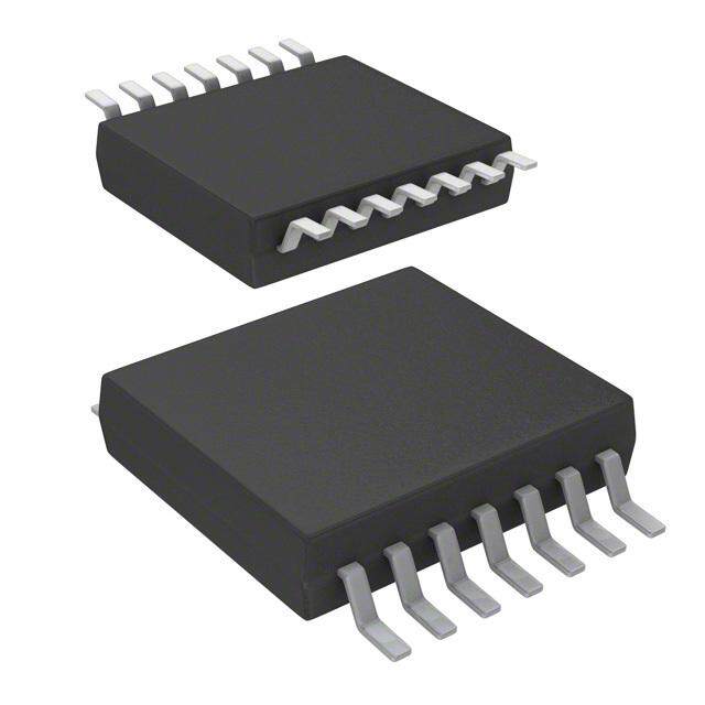
| 产品图片 |
|
| 产品型号 | TC4069UBFTELN |
| rohs | 无铅 / 符合限制有害物质指令(RoHS)规范要求 |
| 产品系列 | TC |
| 不同V、最大CL时的最大传播延迟 | 50ns @ 15V,50pF |
| 供应商器件封装 | 14-TSSOP |
| 其它名称 | TC4069UBFTELNCT |
| 包装 | 剪切带 (CT) |
| 安装类型 | 表面贴装 |
| 封装/外壳 | 14-TSSOP(0.173",4.40mm 宽) |
| 工作温度 | -40°C ~ 85°C |
| 标准包装 | 1 |
| 特性 | - |
| 电压-电源 | 3 V ~ 18 V |
| 电流-输出高,低 | 3.4mA,3.4mA |
| 电流-静态(最大值) | 1µA |
| 电路数 | 6 |
| 输入数 | 6 |
| 逻辑电平-低 | 1 V ~ 3 V |
| 逻辑电平-高 | 4 V ~ 12 V |
| 逻辑类型 |


- 商务部:美国ITC正式对集成电路等产品启动337调查
- 曝三星4nm工艺存在良率问题 高通将骁龙8 Gen1或转产台积电
- 太阳诱电将投资9.5亿元在常州建新厂生产MLCC 预计2023年完工
- 英特尔发布欧洲新工厂建设计划 深化IDM 2.0 战略
- 台积电先进制程称霸业界 有大客户加持明年业绩稳了
- 达到5530亿美元!SIA预计今年全球半导体销售额将创下新高
- 英特尔拟将自动驾驶子公司Mobileye上市 估值或超500亿美元
- 三星加码芯片和SET,合并消费电子和移动部门,撤换高东真等 CEO
- 三星电子宣布重大人事变动 还合并消费电子和移动部门
- 海关总署:前11个月进口集成电路产品价值2.52万亿元 增长14.8%


PDF Datasheet 数据手册内容提取
TC4069UBP/UBF/UBFT TOSHIBA CMOS Digital Integrated Circuit Silicon Monolithic TC4069UBP, TC4069UBF, TC4069UBFT TC4069UB Hex Inverter TC4069UB contains six circuits of inverters. Since the internal circuit is composed of a single stage inverter, this is suitable for TC4069UBP the applications of CR oscillator circuits, crystal oscillator circuits and linear amplifiers in addition to its application as inverters. Because of one stage gate configuration, the propagation time has been reduced. Pin Assignment TC4069UBF I1 1 14 VDD O1 2 13 I6 I2 3 12 O6 O2 4 11 I5 I3 5 10 O5 O3 6 9 I4 VSS 7 8 O4 TC4069UBFT (top view) Circuit Diagram 1/6 TC4069UB VDD Weight DIP14-P-300-2.54 : 0.96 g (typ.) SOP14-P-300-1.27A : 0.18 g (typ.) TSSOP14-P-0044-0.65A : 0.06 g (typ.) INPUT OUTPUT VSS Start of commercial production 1978-04 1 2014-03-01
TC4069UBP/UBF/UBFT Absolute Maximum Ratings (Note) Characteristics Symbol Rating Unit DC supply voltage VDD VSS − 0.5 to VSS + 20 V Input voltage VIN VSS − 0.5 to VDD + 0.5 V Output voltage VOUT VSS − 0.5 to VDD + 0.5 V DC input current IIN ±10 mA Power dissipation PD 300 (DIP)/180 (SOP) mW Operating temperature range Topr −40 to 85 °C Storage temperature range Tstg −65 to 150 °C Note: Exceeding any of the absolute maximum ratings, even briefly, lead to deterioration in IC performance or even destruction. Using continuously under heavy loads (e.g. the application of high temperature/current/voltage and the significant change in temperature, etc.) may cause this product to decrease in the reliability significantly even if the operating conditions (i.e. operating temperature/current/voltage, etc.) are within the absolute maximum ratings and the operating ranges. Please design the appropriate reliability upon reviewing the Toshiba Semiconductor Reliability Handbook (“Handling Precautions”/“Derating Concept and Methods”) and individual reliability data (i.e. reliability test report and estimated failure rate, etc). Operating Ranges (V = 0 V) (Note) SS Characteristics Symbol Test Condition Min Typ. Max Unit DC supply voltage VDD ― 3 ― 18 V Input voltage VIN ― 0 ― VDD V Note: The operating ranges must be maintained to ensure the normal operation of the device. Unused inputs must be tied to either V or V . DD SS 2 2014-03-01
TC4069UBP/UBF/UBFT Static Electrical Characteristics (V = 0 V) SS Test Condition −40°C 25°C 85°C Characteristics Symbol Unit VDD Min Max Min Typ. Max Min Max (V) 5 4.95 ⎯ 4.95 5.00 ⎯ 4.95 ⎯ High-level |IOUT| < 1 μA output voltage VOH VIN = VSS, VDD 10 9.95 ⎯ 9.95 10.00 ⎯ 9.95 ⎯ V 15 14.95 ⎯ 14.95 15.00 ⎯ 14.95 ⎯ 5 ⎯ 0.05 ⎯ 0.00 0.05 ⎯ 0.05 Low-level |IOUT| < 1 μA output voltage VOL VIN = VSS, VDD 10 ⎯ 0.05 ⎯ 0.00 0.05 ⎯ 0.05 V 15 ⎯ 0.05 ⎯ 0.00 0.05 ⎯ 0.05 VOH = 4.6 V 5 −0.61 ⎯ −0.51 −1.0 ⎯ −0.42 ⎯ VOH = 2.5 V 5 −2.50 ⎯ −2.10 −4.0 ⎯ −1.70 ⎯ Output high current IOH VOH = 9.5 V 10 −1.50 ⎯ −1.30 −2.2 ⎯ −1.10 ⎯ mA VOH = 13.5 V 15 −4.00 ⎯ −3.40 −9.0 ⎯ −2.80 ⎯ VIN = VSS VOL = 0.4 V 5 0.61 ⎯ 0.51 1.2 ⎯ 0.42 ⎯ Output low VOL = 0.5 V 10 1.50 ⎯ 1.30 3.2 ⎯ 1.10 ⎯ current IOL VOL = 1.5 V 15 4.00 ⎯ 3.40 12.0 ⎯ 2.80 ⎯ mA VIN = VDD VOUT = 0.5 V, 4.5 V 5 4.0 ⎯ 4.0 ⎯ ⎯ 4.0 ⎯ Input high VOUT = 1.0 V, 9.0 V 10 8.0 ⎯ 8.0 ⎯ ⎯ 8.0 ⎯ voltage VIH VOUT = 1.5 V, 13.5 V 15 12.0 ⎯ 12.0 ⎯ ⎯ 12.0 ⎯ V |IOUT| < 1 μA VOUT = 0.5 V, 4.5 V 5 ⎯ 1.0 ⎯ ⎯ 1.0 ⎯ 1.0 Input low VOUT = 1.0 V, 9.0 V 10 ⎯ 2.0 ⎯ ⎯ 2.0 ⎯ 2.0 voltage VIL VOUT = 1.5 V, 13.5 V 15 ⎯ 3.0 ⎯ ⎯ 3.0 ⎯ 3.0 V |IOUT| < 1 μA Input “leHv”e l IIH VIL = 18 V 18 ⎯ 0.1 ⎯ 10−5 0.1 ⎯ 1.0 μA current “leLv” el IIL VIL = 0 V 18 ⎯ −0.1 ⎯ −10−5 −0.1 ⎯ −1.0 5 ⎯ 0.25 ⎯ 0.001 0.25 ⎯ 7.5 Quiescent VIN = VSS, VDD supply current IDD (Note) 10 ⎯ 0.50 ⎯ 0.001 0.50 ⎯ 15.0 μA 15 ⎯ 1.00 ⎯ 0.002 1.00 ⎯ 30.0 Note: All valid input combinations. 3 2014-03-01
TC4069UBP/UBF/UBFT Dynamic Electrical Characteristics (Ta = 25°C, V = 0 V, C = 50 pF) SS L Test Condition Characteristics Symbol Min Typ. Max Unit VDD (V) 5 ⎯ 70 200 Output transition time (low to high) tTLH ⎯ 10 ⎯ 35 100 ns 15 ⎯ 30 80 5 ⎯ 70 200 Output transition time (high to low) tTHL ⎯ 10 ⎯ 35 100 ns 15 ⎯ 30 80 5 ⎯ 55 110 Propagation delay time (low to high) tpLH ⎯ 10 ⎯ 30 60 ns 15 ⎯ 25 50 5 ⎯ 55 110 Propagation delay time (high to low) tpHL ⎯ 10 ⎯ 30 60 ns 15 ⎯ 25 50 Input capacitance CIN ⎯ ⎯ 7.5 15 pF Waveform for Measurement of Dynamic Characteristics 20 ns 20 ns 90% 90% Input 50% 50% 10% 10% tpHL tpLH Output tTHL tTLH 4 2014-03-01
TC4069UBP/UBF/UBFT Package Dimensions Weight: 0.96 g (typ.) 5 2014-03-01
TC4069UBP/UBF/UBFT Package Dimensions Weight: 0.18 g (typ.) 6 2014-03-01
TC4069UBP/UBF/UBFT Package Dimensions Weight: 0.06 g (typ.) 7 2014-03-01
TC4069UBP/UBF/UBFT RESTRICTIONS ON PRODUCT USE • Toshiba Corporation, and its subsidiaries and affiliates (collectively "TOSHIBA"), reserve the right to make changes to the information in this document, and related hardware, software and systems (collectively "Product") without notice. • This document and any information herein may not be reproduced without prior written permission from TOSHIBA. Even with TOSHIBA's written permission, reproduction is permissible only if reproduction is without alteration/omission. • Though TOSHIBA works continually to improve Product's quality and reliability, Product can malfunction or fail. Customers are responsible for complying with safety standards and for providing adequate designs and safeguards for their hardware, software and systems which minimize risk and avoid situations in which a malfunction or failure of Product could cause loss of human life, bodily injury or damage to property, including data loss or corruption. Before customers use the Product, create designs including the Product, or incorporate the Product into their own applications, customers must also refer to and comply with (a) the latest versions of all relevant TOSHIBA information, including without limitation, this document, the specifications, the data sheets and application notes for Product and the precautions and conditions set forth in the "TOSHIBA Semiconductor Reliability Handbook" and (b) the instructions for the application with which the Product will be used with or for. Customers are solely responsible for all aspects of their own product design or applications, including but not limited to (a) determining the appropriateness of the use of this Product in such design or applications; (b) evaluating and determining the applicability of any information contained in this document, or in charts, diagrams, programs, algorithms, sample application circuits, or any other referenced documents; and (c) validating all operating parameters for such designs and applications. TOSHIBA ASSUMES NO LIABILITY FOR CUSTOMERS' PRODUCT DESIGN OR APPLICATIONS. • PRODUCT IS NEITHER INTENDED NOR WARRANTED FOR USE IN EQUIPMENTS OR SYSTEMS THAT REQUIRE EXTRAORDINARILY HIGH LEVELS OF QUALITY AND/OR RELIABILITY, AND/OR A MALFUNCTION OR FAILURE OF WHICH MAY CAUSE LOSS OF HUMAN LIFE, BODILY INJURY, SERIOUS PROPERTY DAMAGE AND/OR SERIOUS PUBLIC IMPACT ("UNINTENDED USE"). Except for specific applications as expressly stated in this document, Unintended Use includes, without limitation, equipment used in nuclear facilities, equipment used in the aerospace industry, medical equipment, equipment used for automobiles, trains, ships and other transportation, traffic signaling equipment, equipment used to control combustions or explosions, safety devices, elevators and escalators, devices related to electric power, and equipment used in finance-related fields. IF YOU USE PRODUCT FOR UNINTENDED USE, TOSHIBA ASSUMES NO LIABILITY FOR PRODUCT. For details, please contact your TOSHIBA sales representative. • Do not disassemble, analyze, reverse-engineer, alter, modify, translate or copy Product, whether in whole or in part. • Product shall not be used for or incorporated into any products or systems whose manufacture, use, or sale is prohibited under any applicable laws or regulations. • The information contained herein is presented only as guidance for Product use. No responsibility is assumed by TOSHIBA for any infringement of patents or any other intellectual property rights of third parties that may result from the use of Product. No license to any intellectual property right is granted by this document, whether express or implied, by estoppel or otherwise. • ABSENT A WRITTEN SIGNED AGREEMENT, EXCEPT AS PROVIDED IN THE RELEVANT TERMS AND CONDITIONS OF SALE FOR PRODUCT, AND TO THE MAXIMUM EXTENT ALLOWABLE BY LAW, TOSHIBA (1) ASSUMES NO LIABILITY WHATSOEVER, INCLUDING WITHOUT LIMITATION, INDIRECT, CONSEQUENTIAL, SPECIAL, OR INCIDENTAL DAMAGES OR LOSS, INCLUDING WITHOUT LIMITATION, LOSS OF PROFITS, LOSS OF OPPORTUNITIES, BUSINESS INTERRUPTION AND LOSS OF DATA, AND (2) DISCLAIMS ANY AND ALL EXPRESS OR IMPLIED WARRANTIES AND CONDITIONS RELATED TO SALE, USE OF PRODUCT, OR INFORMATION, INCLUDING WARRANTIES OR CONDITIONS OF MERCHANTABILITY, FITNESS FOR A PARTICULAR PURPOSE, ACCURACY OF INFORMATION, OR NONINFRINGEMENT. • Do not use or otherwise make available Product or related software or technology for any military purposes, including without limitation, for the design, development, use, stockpiling or manufacturing of nuclear, chemical, or biological weapons or missile technology products (mass destruction weapons). Product and related software and technology may be controlled under the applicable export laws and regulations including, without limitation, the Japanese Foreign Exchange and Foreign Trade Law and the U.S. Export Administration Regulations. Export and re-export of Product or related software or technology are strictly prohibited except in compliance with all applicable export laws and regulations. • Please contact your TOSHIBA sales representative for details as to environmental matters such as the RoHS compatibility of Product. Please use Product in compliance with all applicable laws and regulations that regulate the inclusion or use of controlled substances, including without limitation, the EU RoHS Directive. TOSHIBA ASSUMES NO LIABILITY FOR DAMAGES OR LOSSES OCCURRING AS A RESULT OF NONCOMPLIANCE WITH APPLICABLE LAWS AND REGULATIONS. 8 2014-03-01