ICGOO在线商城 > TC2186-5.0VCTTR
 Datasheet下载
- 型号: TC2186-5.0VCTTR
- 制造商: Microchip
- 库位|库存: xxxx|xxxx
- 要求:
| 数量阶梯 | 香港交货 | 国内含税 |
| +xxxx | $xxxx | ¥xxxx |
查看当月历史价格
查看今年历史价格
TC2186-5.0VCTTR产品简介:
ICGOO电子元器件商城为您提供TC2186-5.0VCTTR由Microchip设计生产,在icgoo商城现货销售,并且可以通过原厂、代理商等渠道进行代购。 提供TC2186-5.0VCTTR价格参考以及MicrochipTC2186-5.0VCTTR封装/规格参数等产品信息。 你可以下载TC2186-5.0VCTTR参考资料、Datasheet数据手册功能说明书, 资料中有TC2186-5.0VCTTR详细功能的应用电路图电压和使用方法及教程。
| 参数 | 数值 |
| 产品目录 | 集成电路 (IC) |
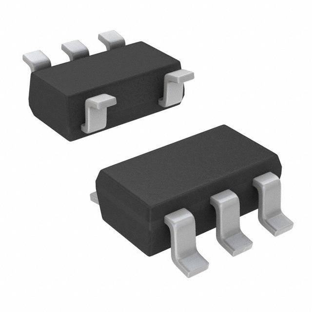
| 描述 | IC REG LDO 5V 0.15A SOT23-5 |
| 产品分类 | |
| 品牌 | Microchip Technology |
| 数据手册 | http://www.microchip.com/mymicrochip/filehandler.aspx?ddocname=en026002http://www.microchip.com/mymicrochip/filehandler.aspx?ddocname=en011457http://www.microchip.com/mymicrochip/filehandler.aspx?ddocname=en023833 |
| 产品图片 |
|
| 产品型号 | TC2186-5.0VCTTR |
| rohs | 无铅 / 符合限制有害物质指令(RoHS)规范要求 |
| 产品系列 | - |
| 产品目录页面 | |
| 供应商器件封装 | SOT-23-5 |
| 其它名称 | TC2186-5.0VCTCT |
| 包装 | 剪切带 (CT) |
| 安装类型 | 表面贴装 |
| 封装/外壳 | SC-74A,SOT-753 |
| 工作温度 | -40°C ~ 125°C |
| 标准包装 | 1 |
| 电压-跌落(典型值) | 0.14V @ 150mA |
| 电压-输入 | 最高 6V |
| 电压-输出 | 5V |
| 电流-输出 | 150mA |
| 电流-限制(最小值) | - |
| 稳压器拓扑 | 正,固定式 |
| 稳压器数 | 1 |


- 商务部:美国ITC正式对集成电路等产品启动337调查
- 曝三星4nm工艺存在良率问题 高通将骁龙8 Gen1或转产台积电
- 太阳诱电将投资9.5亿元在常州建新厂生产MLCC 预计2023年完工
- 英特尔发布欧洲新工厂建设计划 深化IDM 2.0 战略
- 台积电先进制程称霸业界 有大客户加持明年业绩稳了
- 达到5530亿美元!SIA预计今年全球半导体销售额将创下新高
- 英特尔拟将自动驾驶子公司Mobileye上市 估值或超500亿美元
- 三星加码芯片和SET,合并消费电子和移动部门,撤换高东真等 CEO
- 三星电子宣布重大人事变动 还合并消费电子和移动部门
- 海关总署:前11个月进口集成电路产品价值2.52万亿元 增长14.8%


PDF Datasheet 数据手册内容提取
TC2054/2055/2186 50 mA, 100 mA, and 150 mA CMOS LDOs with Shutdown and Error Output Features General Description • Low Supply Current (55µA Typical) for Longer The TC2054, TC2055 and TC2186 are high accuracy Battery Life (typically ±0.4%) CMOS upgrades for older (bipolar) • Low Dropout Voltage: 140mV (Typical) @ low dropout regulators. Designed specifically for 150mA battery-operated systems, the devices’ total supply current is typically 55µA at full load (20 to 60 times • High Output Voltage Accuracy: ±0.4% (Typical) lower than in bipolar regulators). • Standard or Custom Output Voltages The devices’ key features include low noise operation, • Power-Saving Shutdown Mode low dropout voltage – typically 45mV (TC2054); 90mV • ERROR Output Can Be Used as a Low Battery (TC2055); and 140mV (TC2186) at full load - and fast Detector or Processor Reset Generator response to step changes in load. An error output • Fast Shutdown Reponse Time: 60µs (Typical) (ERROR) is asserted when the devices are • Overcurrent and Overtemperature Protection out-of-regulation (due to a low input voltage or • Space-Saving 5-Pin SOT-23A Package excessive output current). Supply current is reduced to 0.5µA (maximum) and both V and ERROR are • Pin Compatible Upgrades for Bipolar Regulators OUT disabled when the shutdown input is low. The devices • Standard Output Voltage Options: also incorporate overcurrent and overtemperature - 1.8V, 2.5V, 2.6V, 2.7V, 2.8V, 2.85V, 3.0V, protection. 3.3V, 5.0V The TC2054, TC2055 and TC2186 are stable with a low esr ceramic output capacitor of 1µF and have a Applications maximum output current of 50mA, 100mA and • Battery Operated Systems 150mA, respectively. This LDO Family also features a • Portable Computers fast response time (60µs typically) when released from shutdown. • Medical Instruments • Instrumentation Package Type • Cellular / GSMS / PHS Phones • Pagers 5-Pin SOT-23A Top View Typical Application VOUT ERROR 5 4 VIN 1 VIN VOUT 5 VOUT TC2054 1µF 1µF TC2055 TC2186 2 GND TC2054 1 2 3 TC2055 1M TC2186 VIN GND SHDN 3 4 SHDN ERROR ERROR Shutdown Control (from Power Control Logic) © 2009 Microchip Technology Inc. DS21663D-page 1
TC2054/2055/2186 NOTES: DS21663D-page 2 © 2009 Microchip Technology Inc.
TC2054/2055/2186 1.0 ELECTRICAL † Notice: Stresses above those listed under “Absolute CHARACTERISTICS Maximum Ratings” may cause permanent damage to the device. These are stress ratings only and functional operation of the device at these or any other conditions Absolute Maximum Ratings † above those indicated in the operation sections of the specifications is not implied. Exposure to Absolute Input Voltage.........................................................6.5V Maximum Rating conditions for extended periods my Output Voltage...............................(-0.3) to (V + 0.3) IN affect device reliability. Operating Temperature..................-40°C < T < 125°C J Storage Temperature.........................-65°C to +150°C Maximum Voltage on Any Pin ........V +0.3V to -0.3V IN ELECTRICAL SPECIFICATIONS Electrical Specifications: Unless otherwise noted, V = V + 1V, I = 100µA, C = 3.3µF, SHDN > V , T = +25°C. IN R L L IH A BOLDFACE type specifications apply for junction temperature of -40°C to +125°C. Parameter Sym Min Typ Max Units Conditions Input Operating Voltage V 2.7 — 6.0 V Note1 IN Maximum Output Current IOUTMAX 50 — — mA TC2054 100 — — TC2055 150 — — TC2186 Output Voltage V V - 2.0% V ± 0.4% V + 2.0% V Note2 OUT R R R V Temperature TCV — 20 — ppm/°C Note3 OUT OUT Coefficient — 40 — Line Regulation ΔV / — 0.05 0.5 % (V + 1V) < V < 6V OUT R IN ΔV IN Load Regulation ΔVOUT/ -1.0 0.33 +1.0 % TC2054;TC2055 IL = 0.1mA to IOUTMAX V OUT -2.0 0.43 +2.0 TC2186 IL = 0.1mA to IOUTMAX Note6 Dropout Voltage, Note7 V – V — 2 — mV I = 100µA IN OUT L — 45 70 I = 50mA L — 90 140 TC2015; TC2185 I = 100mA L — 140 210 TC2185 I = 150mA L Note7 Supply Current I — 55 80 µA SHDN = V , I =0 IN IH L Shutdown Supply Current I — 0.05 0.5 µA SHDN = 0V INSD Power Supply Rejection PSRR — 50 — dB F ≤ 100kHz RE Ratio Output Short Circuit Current I 160 300 — mA V = 0V OUTSC OUT Note 1: The minimum V has to meet two conditions: V = 2.7V and V = V + V . IN IN IN R DROPOUT 2: V is the regulator output voltage setting. For example: V = 1.8V, 2.7V, 2.8V, 2.85V, 3.0V, 3.3V. R R 3: TCVOUT = (V –V )×106 4: -------O-----U-----T----M------A----X--------------O------U----T----M------I--N---------------------- V ×ΔT 5: OUT 6: Regulation is measured at a constant junction temperature using low duty cycle pulse testing. Load regulation is tested over a load range from 1.0mA to the maximum specified output current. Changes in output voltage due to heating effects are covered by the thermal regulation specification. 7: Dropout voltage is defined as the input to output differential at which the output voltage drops 2% below its nominal value at a 1V differential. 8: Thermal Regulation is defined as the change in output voltage at a time T after a change in power dissipation is applied, excluding load or line regulation effects. Specifications are for a current pulse equal to I at V = 6V for T = 10ms. MAX IN 9: The maximum allowable power dissipation is a function of ambient temperature, the maximum allowable junction tem- perature and the thermal resistance from junction-to-air (i.e. T , T , θ ). A J JA 10: Hysteresis voltage is referenced by V . R 11: Time required for V to reach 95% of V (output voltage setting), after V is switched from 0 to V . OUT R SHDN IN © 2009 Microchip Technology Inc. DS21663D-page 3
TC2054/2055/2186 ELECTRICAL SPECIFICATIONS (CONTINUED) Electrical Specifications: Unless otherwise noted, V = V + 1V, I = 100µA, C = 3.3µF, SHDN > V , T = +25°C. IN R L L IH A BOLDFACE type specifications apply for junction temperature of -40°C to +125°C. Parameter Sym Min Typ Max Units Conditions Thermal Regulation ΔV ΔP — 0.04 — V/W Note8 OUT/ D Thermal Shutdown Die T — 160 — °C SD Temperature Output Noise eN — 600 — nV / I = I , F = 10kHz L OUTMAX √Hz Response Time t — 60 — µs V = 4V R IN (from Shutdown Mode) C = 1µF, C = 10µF IN OUT I = 0.1mA, Note11 L SHDN Input SHDN Input High Threshold V 60 — — %V V = 2.5V to 6.0V IH IN IN SHDN Input Low Threshold V — — 15 %V V = 2.5V to 6.0V IL IN IN ERROR OUTPUT Minimum V Operating V 1.0 — — V I = 0.1mA IN INMIN OL Voltage Output Logic Low Voltage V — — 400 mV 1mA Flows to ERROR, OL I = 1mA, V = 2V OL IN ERROR Threshold Voltage V — 0.95 x V — V See Figure4-2 TH R ERROR Positive Hysteresis V — 50 — mV Note10 HYS V to ERROR Delay t — 2 — ms V from V = 3V to 2.8V OUT DELAY OUT R Resistance from ERROR to R — 126 — Ω V = 2.5V, V = 2.5V ERROR DD OUT GND Note 1: The minimum V has to meet two conditions: V = 2.7V and V = V + V . IN IN IN R DROPOUT 2: V is the regulator output voltage setting. For example: V = 1.8V, 2.7V, 2.8V, 2.85V, 3.0V, 3.3V. R R 3: TCVOUT = (V –V )×106 4: -------O-----U-----T----M------A----X--------------O------U----T----M------I--N---------------------- V ×ΔT 5: OUT 6: Regulation is measured at a constant junction temperature using low duty cycle pulse testing. Load regulation is tested over a load range from 1.0mA to the maximum specified output current. Changes in output voltage due to heating effects are covered by the thermal regulation specification. 7: Dropout voltage is defined as the input to output differential at which the output voltage drops 2% below its nominal value at a 1V differential. 8: Thermal Regulation is defined as the change in output voltage at a time T after a change in power dissipation is applied, excluding load or line regulation effects. Specifications are for a current pulse equal to I at V = 6V for T = 10ms. MAX IN 9: The maximum allowable power dissipation is a function of ambient temperature, the maximum allowable junction tem- perature and the thermal resistance from junction-to-air (i.e. T , T , θ ). A J JA 10: Hysteresis voltage is referenced by V . R 11: Time required for V to reach 95% of V (output voltage setting), after V is switched from 0 to V . OUT R SHDN IN TEMPERATURE CHARACTERISTICS Electrical Specifications: Unless otherwise noted, V = +2.7V to +6.0V and V = GND. DD SS Parameters Sym Min Typ Max Units Conditions Temperature Ranges: Extended Temperature Range T -40 — +125 °C A Operating Temperature Range T -40 — +125 °C A Storage Temperature Range T -65 — +150 °C A Thermal Package Resistances: Thermal Resistance, 5L-SOT-23 θ — 255 — °C/W JA DS21663D-page 4 © 2009 Microchip Technology Inc.
TC2054/2055/2186 2.0 TYPICAL PERFORMANCE CURVES Note: The graphs and tables provided following this note are a statistical summary based on a limited number of samples and are provided for informational purposes only. The performance characteristics listed herein are not tested or guaranteed. In some graphs or tables, the data presented may be outside the specified operating range (e.g., outside specified power supply range) and therefore outside the warranted range. Note: Unless otherwise indicated, V = V + 1V, I = 100µA, C = 3.3µF, SHDN > V , T = +25°C. IN R L OUT IH A 0 0 VINDC = 4V IOUT= 100 µA VINDC = 4V -20 VVIONUATCD C= =1 030V mVp-p COUT = 1 µF Ceramic -20 VVIONUATCD C= =1 030V mVp-p dB) -40 dB) -40 R ( R ( SR -60 SR -60 P P -80 -80 IOUT= 150 mA COUT = 10 µF Ceramic -100 -100 1100 110000 11,000000 110,00k00 11000,00k00 1,0010M,000 1100 110000 11,000000 110,00k00 11000,00k00 1,0100M,000 f (Hz) f (Hz) FIGURE 2-1: Power Supply Rejection FIGURE 2-4: Power Supply Rejection Ratio. Ratio. 0 0 VINDC = 4V VINDC = 4V -20 VVIONUATCD C= =1 030V mVp-p -20 VVIONUATCD C= =1 030V mVp-p dB) -40 dB) -40 R ( R ( SR -60 SR -60 P P -80 IOUT = 150 mA -80 IOUT= 150 mA COUT = 1 µF Ceramic COUT = 10 µF Tantalum -100 -100 1100 110000 110,00000 101,00k00 11000,00k00 1,0100M,000 1100 110000 11,000000 110,00k00 110000,0k00 1,0100M,000 f (Hz) f (Hz) FIGURE 2-2: Power Supply Rejection FIGURE 2-5: Power Supply Rejection Ratio. Ratio. 0.160 10 VOUT = 1.8V 0.140 0.120 z) 1 H √ C = 1 µF 0.100 T = 25°C oise (µV/ 0.1 OUT DOV (V)00..008600 T = 130°C T = -45°C N 0.01 0.040 0.020 0.001 0.01 0.1 1 10 100 1000 0.000 0 50 100 150 Frequency (kHz) ILOAD (mA) FIGURE 2-3: Output Noise vs. Frequency. FIGURE 2-6: Dropout Voltage vs. I . LOAD © 2009 Microchip Technology Inc. DS21663D-page 5
TC2054/2055/2186 Note: Unless otherwise indicated, V = V + 1V, I = 100µA, C = 3.3µF, SHDN > V , T = +25°C. IN R L OUT IH A 65.00 1.9 VOUT = 1.8V 1.88 63.00 1.86 61.00 1.84 I (μA)DD 59.00 VIN = 2.8V V(V)OUT 11.8.82 VIN = 2.8V 1.78 57.00 1.76 1.74 55.00 1.72 1.7 53.00 -45 5 55 105 155 0 15 30 45 60 7 5 9 0 1 0 5 1 2 0 135 150 Temperature (°C) ILOAD (mA) FIGURE 2-7: I vs. Temperature. FIGURE 2-10: Output Voltage vs. Output DD Current. 2.9 2.9 2.85 IVOOUUT T= = 0 2.1.8mVA VIN = 6.5V 2.85 IVOOUUT T= = 0 2.1.8mVA Temp = +130˚C 2.8 2.8 V(V)OUT 222..67.755 VIN = 3.8V VIN = 6.0V V(V)OUT 222..76.755 Temp = -45˚C Temp = +25˚C 2.6 2.6 2.55 2.55 2.5 2.5 -50 -35 -20 -5 10 2 5 4 0 5 5 7 0 8 5 1 0 0 1 1 5 1 3 0 145 3.5 4 4.5 5 5. 5 6 6 .5 7 Temperature (˚C) VIN (V) FIGURE 2-8: Output Voltage vs. FIGURE 2-11: Output Voltage vs. Supply Temperature. Voltage. 11.8.98 IVOOUUT T= = 0 1.1.8mVA 1.18.89 IVOOUUT T= = 0 1.1.8mVA 1.86 1.86 1.84 1.84 V(V)OUT 111..87.828 VIN = 6V.0INV = 2.8VVIN = 6.5V V(V)OUT 11..178.828 TeTmepm =p +=2 +51˚C30˚C Temp = -45˚C 1.76 1.76 1.74 1.74 1.72 1.72 1.7 1.7 -50 -35 -20 -5 10 2 5 4 0 5 5 7 0 8 5 1 0 0 1 1 5 1 3 0 145 2.7 3.2 3 . 7 4. 2 4.7 5. 2 5.7 6.2 6.7 Temperature (˚C) VIN (V) FIGURE 2-9: Output Voltage vs. FIGURE 2-12: Dropout Voltage vs. Supply Temperature. Voltage. DS21663D-page 6 © 2009 Microchip Technology Inc.
TC2054/2055/2186 Note: Unless otherwise indicated, V = V + 1V, I = 100µA, C = 3.3µF, SHDN > V , T = +25°C. IN R L OUT IH A V I N = 3.8V V I N = 3.0V V O U T = 2.8V V O U T = 2.8V CC IO N U = T 1= μ1F μ CF eCraemraimcic CC IO N U = T 1=μ 1F0 CμFe rCameriacmic Frequency = 1 KHz Frequency = 10KHz 100mV/DIV V O U T 100mV / DIV V O U T Load Current Load Current 1L150o00amμdAA 1L150o00amμdAA FIGURE 2-13: Load Transient Response. FIGURE 2-16: Load Transient Response. Load Transient Response in Dropout Mode V I N = 4.0V VCC O O B U Y U T P T === 310.0.00μV1FμF VOUT I O U T = 100μA 100mV/DIV VSHDN 150mA VIN = 3.105V VOUT = 3.006V CCIONU =T =1 μ1Fμ FC eCrearmamicic 100μA RLOAD = 20Ω VOUT FIGURE 2-14: Load Transient Response in FIGURE 2-17: Shutdown Delay. Dropout Mode. VC O O U U T T == 21.μ8FV Ceramic VSHDN CI O B UY TP == 140700μpAF 50mV / DIV VOUT 2V / DIV Input Voltage 6V VOUT 4V V I N = 4.0V V O U T = 3.0V C O U T = 10μF C B Y P = 0.01μF I O U T = 100μA FIGURE 2-15: Line Transient Response. FIGURE 2-18: Shutdown Wake-up Time. © 2009 Microchip Technology Inc. DS21663D-page 7
TC2054/2055/2186 Note: Unless otherwise indicated, V = V + 1V, I = 100µA, C = 3.3µF, SHDN > V , T = +25°C. IN R L OUT IH A RPULLUP= 100kΩ IOUT=0.3mA VIN 1V/Div 3.42V 2.8V VOUT 1V/Div 3.0V 2.8V VERROR2V/Div 0V FIGURE 2-19: V to ERROR Delay. OUT DS21663D-page 8 © 2009 Microchip Technology Inc.
TC2054/2055/2186 3.0 PIN DESCRIPTIONS The descriptions of the pins are listed in Table3-1. TABLE 3-1: PIN FUNCTION TABLE Pin Number Symbol Description 1 V Unregulated supply input. IN 2 GND Ground terminal. 3 SHDN Shutdown control input. The regulator is fully enabled when a logic high is applied to this input. The regulator enters shutdown when a logic low is applied to this input. During shutdown, output voltage falls to zero, ERROR is open circuited and supply current is reduced to 0.5µA (maximum). 4 ERROR Out-of-Regulation Flag. (Open-drain output). This output goes low when V is OUT out-of-tolerance by approximately -5%. 5 V Regulated voltage output. OUT 3.1 Unregulated Supply Input (V ) 3.4 Out-of-Regulation Flag (ERROR) IN Connect the unregulated input supply to the V pin. If The open-drain ERROR flag provides indication that IN there is a large distance between the input supply and the regulator output voltage is not in regulation. The the LDO regulator, some input capacitance is ERROR pin will be low when the output is typically necessary for proper operation. A 1µF capacitor, below 5% of its specified value. connected from V to ground, is recommended for IN most applications. 3.5 Regulated Voltage Output (V ) OUT 3.2 Ground Terminal (GND) Connect the output load to VOUT of the LDO. Also connect one side of the LDO output decoupling Connect the unregulated input supply ground return to capacitor as close as possible to the V pin. OUT GND. Also connect one side of the 1µF typical input decoupling capacitor close to this pin and one side of the output capacitor C to this pin. OUT 3.3 Shutdown Control Input (SHDN) The regulator is fully enabled when a logic-high is applied to SHDN. The regulator enters shutdown when a logic-low is applied to this input. During shutdown, the output voltage falls to zero and the supply current is reduced to 0.5µA (maximum). © 2009 Microchip Technology Inc. DS21663D-page 9
TC2054/2055/2186 NOTES: DS21663D-page 10 © 2009 Microchip Technology Inc.
TC2054/2055/2186 4.0 DETAILED DESCRIPTION The TC2054, TC2055 and TC2186 are precision fixed VOUT output voltage regulators. (If an adjustable version is desired, refer to the TC1070/TC1071/TC1187 data VTH HYSTERESIS (VHYS) sheet (DS21353). Unlike bipolar regulators, the TC2054, TC2055 and TC2186 supply current does not increase with load current. In addition, V remains ERROR OUT stable and within regulation over the entire 0mA to VIH maximum output current operating load range. VOL Figure4-1 shows a typical application circuit. The regulator is enabled any time the shutdown input FIGURE 4-2: Error Output Operation. (SHDN) is at or above V , and shutdown (disabled) IH when SHDN is at or below VIL. SHDN may be 4.2 Output Capacitor controlled by a CMOS logic gate, or I/O port of a microcontroller. If the SHDN input is not required, it A 1µF (minimum) capacitor from VOUT to ground is should be connected directly to the input supply. While required. The output capacitor should have an effective in shutdown, supply current decreases to 0.05µA series resistance of 0.01Ω. to 5Ω for VOUT = 2.5V, and (typical), VOUT falls to zero volts, and ERROR is 0.05Ω. to 5Ω for VOUT < 2.5V. Ceramic, tantalum and open-circuited. aluminum electrolytic capacitors can be used. (Since many aluminum electrolytic capacitors freeze at approximately -30°C, solid tantalums are VIN VOUT 1µF VOUT recommended for applications operating below -25°C). 1µF When operating from sources other than batteries, C1 supply-noise rejection and transient response can be BATTERY TC2054 improved by increasing the value of the input and GND TC2055 TC2186 output capacitors and employing passive filtering V+ techniques. SHDN ERROR Shutdown Control R1 4.3 Input Capacitor (to CMOS Logic or Tie C2 Requir ed Only 1MΩ BATTL OW to VIN if unused) Pirfo EcResRs(OoSrRe Re isE T SuesxEetT)d S aisg naa l 0C.22µF or RESET Aif 1thµeFre c aisp amcoitroer sthhaonu ld1 0b ei nccohnense cotfe dw firreo mb eVtIwN etoe nG NthDe regulator and this AC filter capacitor, or if a battery is used as the power source. Aluminum electrolytic or FIGURE 4-1: Typical Application Circuit. tantalum capacitors can be used (since many aluminum electrolytic capacitors freeze at 4.1 ERROR Open-Drain Output approximately -30°C, solid tantalum are recommended for applications operating below -25°C). When ERROR is driven low whenever V falls out of OUT operating from sources other than batteries, regulation by more than -5% (typical). This condition supply-noise rejection and transient response can be may be caused by low input voltage, output current improved by increasing the value of the input and limiting or thermal limiting. The ERROR threshold is 5% output capacitors and employing passive filtering below rated V regardless of the programmed OUT techniques. output voltage value (e.g. ERROR = V at 4.75V OL (typical) for a 5.0V regulator and 2.85V (typical) for a 3.0V regulator). ERROR output operation is shown in Figure4-2. Note that ERROR is active when V falls to V , and OUT TH inactive when V rises above V by V . OUT TH HYS As shown in Figure4-1, ERROR can be used as a battery low flag or as a processor RESET signal (with the addition of timing capacitor C ). R x C should be 2 1 2 chosen to maintain ERROR below V of the processor IH RESET input for at least 200ms to allow time for the system to stabilize. Pull-up resistor R can be tied to 1 V , V or any other voltage less than (V + 0.3V). OUT IN IN The ERROR pin sink current is self-limiting to approximately 18mA. © 2009 Microchip Technology Inc. DS21663D-page 11
TC2054/2055/2186 NOTES: DS21663D-page 12 © 2009 Microchip Technology Inc.
TC2054/2055/2186 5.0 THERMAL CONSIDERATIONS Equation5-1 can be used in conjunction with Equation5-2 to ensure regulator thermal operation is 5.1 Thermal Shutdown within limits. For example: Integrated thermal protection circuitry shuts the Given: regulator off when the die temperature exceeds V = 3.0V +10% INMAX approximately 160°C. The regulator remains off until V = 2.7V – 2.5% the die temperature cools to approximatley 150°C. OUTMIN I = 40mA LOADMAX 5.2 Power Dissipation T = +55°C AMAX The amount of power the regulator dissipates is primarily a function of input and output voltage, and Find: output current. 1. Actual power dissipation Equation5-1 is used to calculate worst case power 2. Maximum allowable dissipation dissipation: EQUATION 5-1: Actual power dissipation: P ≈(V –V )I D INMAX OUTMIN LOADMAX P = (V –V )I D INMAX OUTMIN LOADMAX Where: –3 = [(3.0×1.1)–(2.7×0.975)]40×10 P = Worst-case actual power dissipation D = 26.7mW V = Maximum voltage on V INMAX IN Maximum allowable power dissipation: V = Minimum regulator output voltage OUTMIN I = Maximum output (load) current LOADMAX T –T P = ----J--M-----A---X------------A----M----A---X-- DMAX θ The maximum allowable power dissipation JA (Equation5-2) is a function of the maximum ambient 125–55 temperature (TAMAX), the maximum allowable die = ------2----2---0-------- temperature (125 °C) and the thermal resistance from = 318mW junction-to-air (θ ). The 5-Pin SOT-23A package has JA a θ of approximately 220°C/Watt when mounted on a JA In this example, the TC2054 dissipates a maximum of typical two layer FR4 dielectric copper clad PC board. only 26.7mW; far below the allowable limit of 318mW. In a similar manner, Equation5-1 and Equation5-2 can EQUATION 5-2: be used to calculate maximum current and/or input T –T voltage limits. P = ----J--M-----A---X------------A----M----A---X-- DMAX θ JA 5.3 Layout Considerations Where all terms are previously defined. The primary path of heat conduction out of the package is via the package leads. Therefore, layouts having a ground plane, wide traces at the pads, and wide power supply bus lines combine to lower θ and, therefore, JA increase the maximum allowable power dissipation limit. © 2009 Microchip Technology Inc. DS21663D-page 13
TC2054/2055/2186 NOTES: DS21663D-page 14 © 2009 Microchip Technology Inc.
TC2054/2055/2186 6.0 PACKAGING INFORMATION 6.1 Package Marking Information 5-Lead SOT-23 Example: TABLE 6-1: PART NUMBER CODE AND 5 4 TEMPERATURE RANGE 5 4 (V) TC2054 TC2055 TC2186 XXNN SA25 1.8 SA TA VA 2.5 SB TB VB 1 2 3 1 2 3 2.6 SH TH VH 2.7 SC TC VC 2.8 SD TD VD 2.85 SE TE VE 3.0 SF TF VF 3.3 SG TG VG 5.0 SK TJ VJ Legend: XX...X Customer-specific information NN Alphanumeric traceability code 6.2 Taping Information Component Taping Orientation for 5-Pin SOT-23A (EIAJ SC-74A) Devices User Direction of Feed Device Marking W PIN 1 P Standard Reel Component Orientation for 713 Suffix Device (Mark Right Side Up) Carrier Tape, Number of Components Per Reel and Reel Size: Package Carrier Width (W) Pitch (P) Part Per Full Reel Reel Size 5-Pin SOT-23A 8mm 4mm 3000 7 in. © 2009 Microchip Technology Inc. DS21663D-page 15
TC2054/2055/2186 (cid:2)(cid:3)(cid:4)(cid:5)(cid:6)(cid:7)(cid:8)(cid:9)(cid:10)(cid:6)(cid:11)(cid:12)(cid:13)(cid:14)(cid:8)(cid:15)(cid:16)(cid:6)(cid:10)(cid:10)(cid:8)(cid:17)(cid:18)(cid:12)(cid:10)(cid:13)(cid:19)(cid:5)(cid:8)(cid:20)(cid:21)(cid:6)(cid:19)(cid:11)(cid:13)(cid:11)(cid:12)(cid:22)(cid:21)(cid:8)(cid:23)(cid:24)(cid:20)(cid:25)(cid:8)(cid:26)(cid:15)(cid:17)(cid:20)(cid:3)(cid:27)(cid:28)(cid:29) (cid:30)(cid:22)(cid:12)(cid:5)(cid:31) .(cid:10)(cid:9)(cid:2)$(cid:11)(cid:14)(cid:2) (cid:10)!$(cid:2)(cid:8)%(cid:9)(cid:9)(cid:14)(cid:15)$(cid:2)(cid:12)(cid:28)(cid:8)/(cid:28)(cid:17)(cid:14)(cid:2)"(cid:9)(cid:28)-(cid:7)(cid:15)(cid:17)!0(cid:2)(cid:12)(cid:16)(cid:14)(cid:28)!(cid:14)(cid:2)!(cid:14)(cid:14)(cid:2)$(cid:11)(cid:14)(cid:2)(cid:6)(cid:7)(cid:8)(cid:9)(cid:10)(cid:8)(cid:11)(cid:7)(cid:12)(cid:2)1(cid:28)(cid:8)/(cid:28)(cid:17)(cid:7)(cid:15)(cid:17)(cid:2)(cid:22)(cid:12)(cid:14)(cid:8)(cid:7)&(cid:7)(cid:8)(cid:28)$(cid:7)(cid:10)(cid:15)(cid:2)(cid:16)(cid:10)(cid:8)(cid:28)$(cid:14)"(cid:2)(cid:28)$(cid:2) (cid:11)$$(cid:12)+22---(cid:20) (cid:7)(cid:8)(cid:9)(cid:10)(cid:8)(cid:11)(cid:7)(cid:12)(cid:20)(cid:8)(cid:10) 2(cid:12)(cid:28)(cid:8)/(cid:28)(cid:17)(cid:7)(cid:15)(cid:17) b N E E1 1 2 3 e e1 D A A2 c φ A1 L L1 3(cid:15)(cid:7)$! (cid:6)(cid:19)44(cid:19)(cid:6)#(cid:13)#(cid:26)(cid:22) (cid:21)(cid:7) (cid:14)(cid:15)!(cid:7)(cid:10)(cid:15)(cid:2)4(cid:7) (cid:7)$! (cid:6)(cid:19)5 56(cid:6) (cid:6)(cid:25)7 5% 8(cid:14)(cid:9)(cid:2)(cid:10)&(cid:2)1(cid:7)(cid:15)! 5 (cid:30) 4(cid:14)(cid:28)"(cid:2)1(cid:7)$(cid:8)(cid:11) (cid:14) (cid:4)(cid:20)(cid:24)(cid:30)(cid:2))(cid:22)* 6%$!(cid:7)"(cid:14)(cid:2)4(cid:14)(cid:28)"(cid:2)1(cid:7)$(cid:8)(cid:11) (cid:14)(cid:31) (cid:31)(cid:20)(cid:24)(cid:4)(cid:2))(cid:22)* 6,(cid:14)(cid:9)(cid:28)(cid:16)(cid:16)(cid:2)9(cid:14)(cid:7)(cid:17)(cid:11)$ (cid:25) (cid:4)(cid:20)(cid:24)(cid:4) : (cid:31)(cid:20)(cid:23)(cid:30) (cid:6)(cid:10)(cid:16)"(cid:14)"(cid:2)1(cid:28)(cid:8)/(cid:28)(cid:17)(cid:14)(cid:2)(cid:13)(cid:11)(cid:7)(cid:8)/(cid:15)(cid:14)!! (cid:25)(cid:3) (cid:4)(cid:20);(cid:24) : (cid:31)(cid:20)(cid:29)(cid:4) (cid:22)$(cid:28)(cid:15)"(cid:10)&& (cid:25)(cid:31) (cid:4)(cid:20)(cid:4)(cid:4) : (cid:4)(cid:20)(cid:31)(cid:30) 6,(cid:14)(cid:9)(cid:28)(cid:16)(cid:16)(cid:2)<(cid:7)"$(cid:11) # (cid:3)(cid:20)(cid:3)(cid:4) : (cid:29)(cid:20)(cid:3)(cid:4) (cid:6)(cid:10)(cid:16)"(cid:14)"(cid:2)1(cid:28)(cid:8)/(cid:28)(cid:17)(cid:14)(cid:2)<(cid:7)"$(cid:11) #(cid:31) (cid:31)(cid:20)(cid:29)(cid:4) : (cid:31)(cid:20);(cid:4) 6,(cid:14)(cid:9)(cid:28)(cid:16)(cid:16)(cid:2)4(cid:14)(cid:15)(cid:17)$(cid:11) (cid:21) (cid:3)(cid:20)(cid:5)(cid:4) : (cid:29)(cid:20)(cid:31)(cid:4) .(cid:10)(cid:10)$(cid:2)4(cid:14)(cid:15)(cid:17)$(cid:11) 4 (cid:4)(cid:20)(cid:31)(cid:4) : (cid:4)(cid:20)=(cid:4) .(cid:10)(cid:10)$(cid:12)(cid:9)(cid:7)(cid:15)$ 4(cid:31) (cid:4)(cid:20)(cid:29)(cid:30) : (cid:4)(cid:20);(cid:4) .(cid:10)(cid:10)$(cid:2)(cid:25)(cid:15)(cid:17)(cid:16)(cid:14) (cid:3) (cid:4)> : (cid:29)(cid:4)> 4(cid:14)(cid:28)"(cid:2)(cid:13)(cid:11)(cid:7)(cid:8)/(cid:15)(cid:14)!! (cid:8) (cid:4)(cid:20)(cid:4); : (cid:4)(cid:20)(cid:3)= 4(cid:14)(cid:28)"(cid:2)<(cid:7)"$(cid:11) 8 (cid:4)(cid:20)(cid:3)(cid:4) : (cid:4)(cid:20)(cid:30)(cid:31) (cid:30)(cid:22)(cid:12)(cid:5)(cid:11)(cid:31) (cid:31)(cid:20) (cid:21)(cid:7) (cid:14)(cid:15)!(cid:7)(cid:10)(cid:15)!(cid:2)(cid:21)(cid:2)(cid:28)(cid:15)"(cid:2)#(cid:31)(cid:2)"(cid:10)(cid:2)(cid:15)(cid:10)$(cid:2)(cid:7)(cid:15)(cid:8)(cid:16)%"(cid:14)(cid:2) (cid:10)(cid:16)"(cid:2)&(cid:16)(cid:28)!(cid:11)(cid:2)(cid:10)(cid:9)(cid:2)(cid:12)(cid:9)(cid:10)$(cid:9)%!(cid:7)(cid:10)(cid:15)!(cid:20)(cid:2)(cid:6)(cid:10)(cid:16)"(cid:2)&(cid:16)(cid:28)!(cid:11)(cid:2)(cid:10)(cid:9)(cid:2)(cid:12)(cid:9)(cid:10)$(cid:9)%!(cid:7)(cid:10)(cid:15)!(cid:2)!(cid:11)(cid:28)(cid:16)(cid:16)(cid:2)(cid:15)(cid:10)$(cid:2)(cid:14)’(cid:8)(cid:14)(cid:14)"(cid:2)(cid:4)(cid:20)(cid:31)(cid:3)(cid:5)(cid:2) (cid:2)(cid:12)(cid:14)(cid:9)(cid:2)!(cid:7)"(cid:14)(cid:20) (cid:3)(cid:20) (cid:21)(cid:7) (cid:14)(cid:15)!(cid:7)(cid:10)(cid:15)(cid:7)(cid:15)(cid:17)(cid:2)(cid:28)(cid:15)"(cid:2)$(cid:10)(cid:16)(cid:14)(cid:9)(cid:28)(cid:15)(cid:8)(cid:7)(cid:15)(cid:17)(cid:2)(cid:12)(cid:14)(cid:9)(cid:2)(cid:25)(cid:22)(cid:6)#(cid:2)((cid:31)(cid:23)(cid:20)(cid:30)(cid:6)(cid:20) )(cid:22)*+ )(cid:28)!(cid:7)(cid:8)(cid:2)(cid:21)(cid:7) (cid:14)(cid:15)!(cid:7)(cid:10)(cid:15)(cid:20)(cid:2)(cid:13)(cid:11)(cid:14)(cid:10)(cid:9)(cid:14)$(cid:7)(cid:8)(cid:28)(cid:16)(cid:16)(cid:18)(cid:2)(cid:14)’(cid:28)(cid:8)$(cid:2),(cid:28)(cid:16)%(cid:14)(cid:2)!(cid:11)(cid:10)-(cid:15)(cid:2)-(cid:7)$(cid:11)(cid:10)%$(cid:2)$(cid:10)(cid:16)(cid:14)(cid:9)(cid:28)(cid:15)(cid:8)(cid:14)!(cid:20) (cid:6)(cid:7)(cid:8)(cid:9)(cid:10)(cid:8)(cid:11)(cid:7)(cid:12)(cid:13)(cid:14)(cid:8)(cid:11)(cid:15)(cid:10)(cid:16)(cid:10)(cid:17)(cid:18)(cid:21)(cid:9)(cid:28)-(cid:7)(cid:15)(cid:17)*(cid:4)(cid:23)(cid:27)(cid:4)(cid:24)(cid:31)) DS21663D-page 16 © 2009 Microchip Technology Inc.
TC2054/2055/2186 APPENDIX A: REVISION HISTORY Revision D (September 2009) The following is the list of modifications: 1. Added the 2.6V, and 5.0V option in Table6-1 in Section6.0 “Packaging Information”. 2. Updated the package outline drawing. 3. Added 2.6V option to Product Identification System section. Revision C (May 2006) The following is the list of modifications: 1. Added overtemperature to bullet for overcurrent protection in Features and General Description verbiage. 2. Added “Thermal Shutdown Die Temperature” to the Electrical Specifications table. Changed condition for “Minimum V Operating Voltage”. IN 3. Added Temperature Characteristics Table. 4. Added Section5.1 “Thermal Shutdown”. 5. Updated the package outline drawing. Revision B (May 2002) • Data Sheet converted to Microchip standards. Revision A (May 2001) • Original Release of this Document under Telcom. © 2009 Microchip Technology Inc. DS21663D-page 13
TC2054/2055/2186 NOTES: DS21663D-page 14 © 2009 Microchip Technology Inc.
TC2054/2055/2186 PRODUCT IDENTIFICATION SYSTEM To order or obtain information, e.g., on pricing or delivery, refer to the factory or the listed sales office. PART NO. -XX X XXXX Examples: a) TC2054-1.8VCTTR: 5LD SOT-23-A, 1.8V, Device Output Temperature Package Tape and Reel. Voltage Range b) TC2054-2.85VCTTR:5LD SOT-23-A, 2.85V, Tape and Reel. Device: TC2054: 50mA LDO with Shutdown and ERROR Output c) TC2054-3.3VCTTR: 5LD SOT-23-A, 3.3V, TC2055: 100mA LDO with Shutdown and ERROR Output Tape and Reel. TC2186: 150mA LDO with Shutdown and ERROR Output a) TC2055-1.8VCTTR: 5LD SOT-23-A, 1.8V, Tape and Reel. Output Voltage: XX = 1.8V XX = 2.5V b) TC2055-2.85VCTTR:5LD SOT-23-A, 2.85V, XX = 2.6V Tape and Reel. XX = 2.7V c) TC2055-3.0VCTTR: 5LD SOT-23-A, 3.0V, XX = 2.8V Tape and Reel. XX = 2.85V XX = 3.0V XX = 3.3V a) TC2186-1.8VCTTR: 5LD SOT-23-A, 1.8V, XX = 5.0V Tape and Reel. b) TC2186-2.8VCTTR: 5LD SOT-23-A, 2.8V, Tape and Reel. Temperature Range: V = -40°C to +125°C Package: CTTR = Plastic Small Outline Transistor (SOT-23), 5-lead, Tape and Reel © 2009 Microchip Technology Inc. DS21663D-page 15
TC2054/2055/2186 NOTES: DS21663D-page 16 © 2009 Microchip Technology Inc.
Note the following details of the code protection feature on Microchip devices: • Microchip products meet the specification contained in their particular Microchip Data Sheet. • Microchip believes that its family of products is one of the most secure families of its kind on the market today, when used in the intended manner and under normal conditions. • There are dishonest and possibly illegal methods used to breach the code protection feature. All of these methods, to our knowledge, require using the Microchip products in a manner outside the operating specifications contained in Microchip’s Data Sheets. Most likely, the person doing so is engaged in theft of intellectual property. • Microchip is willing to work with the customer who is concerned about the integrity of their code. • Neither Microchip nor any other semiconductor manufacturer can guarantee the security of their code. Code protection does not mean that we are guaranteeing the product as “unbreakable.” Code protection is constantly evolving. We at Microchip are committed to continuously improving the code protection features of our products. Attempts to break Microchip’s code protection feature may be a violation of the Digital Millennium Copyright Act. If such acts allow unauthorized access to your software or other copyrighted work, you may have a right to sue for relief under that Act. Information contained in this publication regarding device Trademarks applications and the like is provided only for your convenience The Microchip name and logo, the Microchip logo, dsPIC, and may be superseded by updates. It is your responsibility to KEELOQ, KEELOQ logo, MPLAB, PIC, PICmicro, PICSTART, ensure that your application meets with your specifications. rfPIC and UNI/O are registered trademarks of Microchip MICROCHIP MAKES NO REPRESENTATIONS OR Technology Incorporated in the U.S.A. and other countries. WARRANTIES OF ANY KIND WHETHER EXPRESS OR IMPLIED, WRITTEN OR ORAL, STATUTORY OR FilterLab, Hampshire, HI-TECH C, Linear Active Thermistor, OTHERWISE, RELATED TO THE INFORMATION, MXDEV, MXLAB, SEEVAL and The Embedded Control INCLUDING BUT NOT LIMITED TO ITS CONDITION, Solutions Company are registered trademarks of Microchip QUALITY, PERFORMANCE, MERCHANTABILITY OR Technology Incorporated in the U.S.A. FITNESS FOR PURPOSE. Microchip disclaims all liability Analog-for-the-Digital Age, Application Maestro, CodeGuard, arising from this information and its use. Use of Microchip dsPICDEM, dsPICDEM.net, dsPICworks, dsSPEAK, ECAN, devices in life support and/or safety applications is entirely at ECONOMONITOR, FanSense, HI-TIDE, In-Circuit Serial the buyer’s risk, and the buyer agrees to defend, indemnify and Programming, ICSP, Mindi, MiWi, MPASM, MPLAB Certified hold harmless Microchip from any and all damages, claims, logo, MPLIB, MPLINK, mTouch, Octopus, Omniscient Code suits, or expenses resulting from such use. No licenses are Generation, PICC, PICC-18, PICDEM, PICDEM.net, PICkit, conveyed, implicitly or otherwise, under any Microchip PICtail, PIC32 logo, REAL ICE, rfLAB, Select Mode, Total intellectual property rights. Endurance, TSHARC, UniWinDriver, WiperLock and ZENA are trademarks of Microchip Technology Incorporated in the U.S.A. and other countries. SQTP is a service mark of Microchip Technology Incorporated in the U.S.A. All other trademarks mentioned herein are property of their respective companies. © 2009, Microchip Technology Incorporated, Printed in the U.S.A., All Rights Reserved. Printed on recycled paper. Microchip received ISO/TS-16949:2002 certification for its worldwide headquarters, design and wafer fabrication facilities in Chandler and Tempe, Arizona; Gresham, Oregon and design centers in California and India. The Company’s quality system processes and procedures are for its PIC® MCUs and dsPIC® DSCs, KEELOQ® code hopping devices, Serial EEPROMs, microperipherals, nonvolatile memory and analog products. In addition, Microchip’s quality system for the design and manufacture of development systems is ISO 9001:2000 certified. © 2009 Microchip Technology Inc. DS21663D-page 17
WORLDWIDE SALES AND SERVICE AMERICAS ASIA/PACIFIC ASIA/PACIFIC EUROPE Corporate Office Asia Pacific Office India - Bangalore Austria - Wels 2355 West Chandler Blvd. Suites 3707-14, 37th Floor Tel: 91-80-3090-4444 Tel: 43-7242-2244-39 Chandler, AZ 85224-6199 Tower 6, The Gateway Fax: 91-80-3090-4080 Fax: 43-7242-2244-393 Tel: 480-792-7200 Harbour City, Kowloon India - New Delhi Denmark - Copenhagen Fax: 480-792-7277 Hong Kong Tel: 91-11-4160-8631 Tel: 45-4450-2828 Technical Support: Tel: 852-2401-1200 Fax: 91-11-4160-8632 Fax: 45-4485-2829 http://support.microchip.com Web Address: Fax: 852-2401-3431 India - Pune France - Paris www.microchip.com Australia - Sydney Tel: 91-20-2566-1512 Tel: 33-1-69-53-63-20 Tel: 61-2-9868-6733 Fax: 33-1-69-30-90-79 Fax: 91-20-2566-1513 Atlanta Fax: 61-2-9868-6755 Germany - Munich Duluth, GA Japan - Yokohama China - Beijing Tel: 49-89-627-144-0 Tel: 678-957-9614 Tel: 81-45-471- 6166 Tel: 86-10-8528-2100 Fax: 49-89-627-144-44 Fax: 678-957-1455 Fax: 81-45-471-6122 Fax: 86-10-8528-2104 Italy - Milan Boston Korea - Daegu Westborough, MA China - Chengdu Tel: 82-53-744-4301 Tel: 39-0331-742611 Tel: 774-760-0087 Tel: 86-28-8665-5511 Fax: 82-53-744-4302 Fax: 39-0331-466781 Fax: 774-760-0088 Fax: 86-28-8665-7889 Korea - Seoul Netherlands - Drunen Chicago China - Hong Kong SAR Tel: 82-2-554-7200 Tel: 31-416-690399 Itasca, IL Tel: 852-2401-1200 Fax: 82-2-558-5932 or Fax: 31-416-690340 Tel: 630-285-0071 Fax: 852-2401-3431 82-2-558-5934 Spain - Madrid Fax: 630-285-0075 China - Nanjing Malaysia - Kuala Lumpur Tel: 34-91-708-08-90 Cleveland Tel: 86-25-8473-2460 Tel: 60-3-6201-9857 Fax: 34-91-708-08-91 Independence, OH Fax: 86-25-8473-2470 Fax: 60-3-6201-9859 UK - Wokingham Tel: 216-447-0464 China - Qingdao Malaysia - Penang Tel: 44-118-921-5869 Fax: 216-447-0643 Tel: 86-532-8502-7355 Tel: 60-4-227-8870 Fax: 44-118-921-5820 Dallas Fax: 86-532-8502-7205 Fax: 60-4-227-4068 Addison, TX China - Shanghai Philippines - Manila Tel: 972-818-7423 Tel: 86-21-5407-5533 Tel: 63-2-634-9065 Fax: 972-818-2924 Fax: 86-21-5407-5066 Fax: 63-2-634-9069 Detroit China - Shenyang Singapore Farmington Hills, MI Tel: 86-24-2334-2829 Tel: 65-6334-8870 Tel: 248-538-2250 Fax: 86-24-2334-2393 Fax: 65-6334-8850 Fax: 248-538-2260 China - Shenzhen Taiwan - Hsin Chu Kokomo Tel: 86-755-8203-2660 Tel: 886-3-6578-300 Kokomo, IN Fax: 86-755-8203-1760 Fax: 886-3-6578-370 Tel: 765-864-8360 Fax: 765-864-8387 China - Wuhan Taiwan - Kaohsiung Tel: 86-27-5980-5300 Tel: 886-7-536-4818 Los Angeles Fax: 86-27-5980-5118 Fax: 886-7-536-4803 Mission Viejo, CA Tel: 949-462-9523 China - Xiamen Taiwan - Taipei Fax: 949-462-9608 Tel: 86-592-2388138 Tel: 886-2-2500-6610 Fax: 86-592-2388130 Fax: 886-2-2508-0102 Santa Clara Santa Clara, CA China - Xian Thailand - Bangkok Tel: 408-961-6444 Tel: 86-29-8833-7252 Tel: 66-2-694-1351 Fax: 408-961-6445 Fax: 86-29-8833-7256 Fax: 66-2-694-1350 Toronto China - Zhuhai Mississauga, Ontario, Tel: 86-756-3210040 Canada Fax: 86-756-3210049 Tel: 905-673-0699 Fax: 905-673-6509 03/26/09 DS21663D-page 18 © 2009 Microchip Technology Inc.
Mouser Electronics Authorized Distributor Click to View Pricing, Inventory, Delivery & Lifecycle Information: M icrochip: TC2054-5.0VCTTR TC2055-5.0VCTTR TC2186-5.0VCTTR