ICGOO在线商城 > 集成电路(IC) > 数据采集 - 数模转换器 > TC1320EOA
 Datasheet下载
- 型号: TC1320EOA
- 制造商: Microchip
- 库位|库存: xxxx|xxxx
- 要求:
| 数量阶梯 | 香港交货 | 国内含税 |
| +xxxx | $xxxx | ¥xxxx |
查看当月历史价格
查看今年历史价格
TC1320EOA产品简介:
ICGOO电子元器件商城为您提供TC1320EOA由Microchip设计生产,在icgoo商城现货销售,并且可以通过原厂、代理商等渠道进行代购。 TC1320EOA价格参考¥询价-¥询价。MicrochipTC1320EOA封装/规格:数据采集 - 数模转换器, 8 位 数模转换器 1 8-SOIC。您可以下载TC1320EOA参考资料、Datasheet数据手册功能说明书,资料中有TC1320EOA 详细功能的应用电路图电压和使用方法及教程。
Microchip Technology的TC1320EOA是一款高性能的数模转换器(DAC),属于数据采集系统中的关键组件。以下是该型号的主要应用场景:

1. 工业自动化与控制
   TC1320EOA适用于工业自动化设备,如可编程逻辑控制器(PLC)和分布式控制系统(DCS)。它能够将数字信号转换为精确的模拟电压或电流输出,用于驱动执行器、调节阀或电机控制器等设备。

2. 测试与测量设备
   在精密测试仪器中,例如信号发生器、示波器校准设备或数据记录仪,TC1320EOA提供高分辨率和低噪声的模拟输出,确保测试结果的准确性。

3. 通信系统
   该DAC可用于通信领域的信号调制与解调,例如生成正弦波、方波或其他复杂波形信号,支持无线通信、音频处理和射频(RF)应用。

4. 医疗设备
   医疗领域中,TC1320EOA可用于患者监护仪、超声波设备或核磁共振成像(MRI)系统中,实现对传感器信号的精确转换和控制。

5. 音频处理与消费电子
   在高品质音频设备中,这款DAC可以将数字音频信号转换为模拟信号,用于耳机放大器、音响系统或家庭影院设备。

6. 汽车电子
   TC1320EOA在汽车行业中可用于车身控制系统、信息娱乐系统以及高级驾驶辅助系统(ADAS),提供稳定且可靠的模拟输出。

7. 电力电子与能源管理
   该器件可用于太阳能逆变器、电池管理系统(BMS)或电源调节装置中,帮助生成精确的控制信号以优化能量转换效率。

总结来说,TC1320EOA凭借其高精度、低功耗和宽工作范围的特点,在需要精确模拟信号输出的各种应用场景中表现出色,广泛应用于工业、通信、医疗、消费电子和汽车等领域。
| 参数 | 数值 |
| 产品目录 | 集成电路 (IC)半导体 |
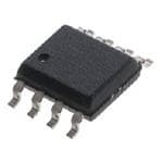
| 描述 | IC DAC 8BIT 2WIRE I2C 8SOIC数模转换器- DAC 8-Bit Two-Wire SOIC8 |
| 产品分类 | |
| 品牌 | Microchip Technology |
| 产品手册 | |
| 产品图片 |
|
| rohs | 符合RoHS无铅 / 符合限制有害物质指令(RoHS)规范要求 |
| 产品系列 | 数据转换器IC,数模转换器- DAC,Microchip Technology TC1320EOA- |
| 数据手册 | http://www.microchip.com/mymicrochip/filehandler.aspx?ddocname=en011565 |
| 产品型号 | TC1320EOA |
| 产品种类 | 数模转换器- DAC |
| 位数 | 8 |
| 供应商器件封装 | 8-SOIC N |
| 分辨率 | 8 bit |
| 包装 | 管件 |
| 商标 | Microchip Technology |
| 安装类型 | 表面贴装 |
| 安装风格 | SMD/SMT |
| 封装 | Tube |
| 封装/外壳 | 8-SOIC(0.154",3.90mm 宽) |
| 封装/箱体 | SOIC-8 |
| 工作温度 | -40°C ~ 85°C |
| 工厂包装数量 | 100 |
| 建立时间 | 10µs |
| 接口类型 | Serial (2-Wire, I2C) |
| 数据接口 | I²C, 串行 |
| 最大工作温度 | + 85 C |
| 最小工作温度 | - 40 C |
| 标准包装 | 100 |
| 电压参考 | External |
| 电压源 | 单电源 |
| 电源电压-最大 | 5.5 V |
| 电源电压-最小 | 2.7 V |
| 积分非线性 | +/- 2 LSB |
| 稳定时间 | 10 us |
| 结构 | Current Steering |
| 转换器数 | 1 |
| 转换器数量 | 1 |
| 输出数和类型 | 1 电压,单极 |
| 输出类型 | Voltage |
| 采样率(每秒) | - |


- 商务部:美国ITC正式对集成电路等产品启动337调查
- 曝三星4nm工艺存在良率问题 高通将骁龙8 Gen1或转产台积电
- 太阳诱电将投资9.5亿元在常州建新厂生产MLCC 预计2023年完工
- 英特尔发布欧洲新工厂建设计划 深化IDM 2.0 战略
- 台积电先进制程称霸业界 有大客户加持明年业绩稳了
- 达到5530亿美元!SIA预计今年全球半导体销售额将创下新高
- 英特尔拟将自动驾驶子公司Mobileye上市 估值或超500亿美元
- 三星加码芯片和SET,合并消费电子和移动部门,撤换高东真等 CEO
- 三星电子宣布重大人事变动 还合并消费电子和移动部门
- 海关总署:前11个月进口集成电路产品价值2.52万亿元 增长14.8%


PDF Datasheet 数据手册内容提取
TC1320 8-Bit Digital-to-Analog Converter with Two-Wire Interface Features General Description • 8-bitDigital-to-AnalogConverter TheTC1320isaseriallyaccessible8-bitvoltageoutput (cid:127) ±2LSBINL digital-to-analog converter (DAC). The DAC produces anoutputvoltagethatrangesfromgroundtoanexter- (cid:127) ±0.8LSBDNL nallysuppliedreferencevoltage.Itoperatesfromasin- (cid:127) 2.7-5.5VSingleSupplyOperation gle power supply that can range from 2.7V to 5.5V, (cid:127) SimpleSMBus/I 2CTMSerialInterface making it ideal for a wide range of applications. Built (cid:127) LowPower:350 µAOperation,0.5µAShutdown intothepartisaPower-onResetfunctionthatensures (cid:127) 8-PinSOICand8-PinMSOPPackages thatthedevicestartsataknowncondition. CommunicationwiththeTC1320isaccomplishedviaa Applications simple2-wireSMBus/I2C™compatibleserialportwith theTC1320actingasaslaveonlydevice.Thehostcan (cid:127) ProgrammableVoltageSources enabletheSHDNbitintheCONFIGregistertoactivate (cid:127) DigitalControlledAmplifiers/Attenuators theLowPowerStandbymode. (cid:127) ProcessMonitoringandControl Package Type Device Selection Table 8-Pin MSOP and Part Temperature 8-Pin SOIC (Narrow) Package Number Range VREF 1 8 VDD TC1320EOA 8-PinSOIC(Narrow) -40°Cto+85°C TC1320EUA 8-PinMSOP -40°Cto+85°C SDA 2 TC1320 7 DAC-OUT SCL 3 6 NC GND 4 5 VOUT Typical Application VIN (8) VDD TC1320 – (1) VOUT VADJUST VREF DAC + (5) Serial Port (3) ((22)) SCLK SDAT Microcontroller 2002MicrochipTechnologyInc. DS21386B-page 1
TC1320 FunctionalBlock Diagram VDD Configuration Register TC1320 SDA Serial Port SCL Interface Control DAC-OUT Data Register DAC VOUT VREF GND DS21386B-page 2 2002MicrochipTechnologyInc.
TC1320 1.0 ELECTRICAL *Stresses above those listed under "Absolute Maximum Ratings"maycausepermanentdamagetothedevice.These CHARACTERISTICS arestressratingsonlyandfunctionaloperationofthedevice attheseoranyotherconditionsabovethoseindicatedinthe Absolute Maximum Ratings* operation sections of the specifications is not implied. Exposure to Absolute Maximum Rating conditions for SupplyVoltage(V ).............................................+6V DD extendedperiodsmayaffectdevicereliability. VoltageonanyPin..(GND–0.3V)to(V +0.3V) DD CurrentonanyPin............................................±50mA PackageThermalResistance(θ )............330°CC/W JA OperatingTemperature(T )........................SeeBelow A StorageTemperature(T )..............-65°Cto+150°C STG TC1320 ELECTRICAL SPECIFICATIONS ElectricalCharacteristics:V =2.7Vto5.5V,-40°C≤T ≤+85°C,V =1.2Vunlessotherwisenoted. DD A REF Symbol Parameter Min Typ Max Unit TestConditions PowerSupply V SupplyVoltage 2.7 350 500 µA DD I OperatingCurrent — 0.35 0.5 mA V =5.5V,V =1.2V DD DD REF SerialPortInactive(Note1) I StandbySupplyCurrent — 0.1 1 µA V =3.3V DD-STANDBY DD SerialPortInactive(Note1) StaticPerformance-AnalogSection Resolution — — 8 Bits INL IntegralNon-LinearityatFS,T =+25°C — — ±2 LSB (Note2) A FSE FullScaleError — — ±3 %FS DNL DifferentialNon-Linearity,T =+25°C — — ±0.8 LSB AllCodes(Note2) A V OffsetErroratV — ±0.3 ±8 mV (Note2) OS OUT TCV OffsetErrorTempcoatV — 10 — µv/°C OS OUT PSRR PowerSupplyRejectionRatio — 80 — dB V atDC DD V VoltageReferenceRange 0 — V –1.2 V REF DD I ReferenceInputLeakageCurrent — — ±1.0 µA REF V VoltageSwing 0 — V V V ≤(V –1.2V) SW REF REF DD R OutputResistance@V — 5 — Ω R (Ω) OUT OUT OUT I OutputCurrent(SourceorSink) — 2 — mA OUT I OutputShort-CircuitCurrent — 30 50 mA Source SC V =5.5V — 20 50 mA Sink DD DynamicPerformance SR VoltageOutputSlewRate — 0.8 — V/µs t OutputVoltageFullScaleSettlingTime — 10 — µsec SETTLE t Wake-upTime — 20 — µs WU DigitalFeedThroughandCrosstalk — 5 — nV-s SDA=V ,SCL=100kHz DD SerialPortInterface V LogicInputHigh 2.4 — V V IH DD V LogicInputLow — — 0.6 — IL V SDAOutputLow — — 0.4 V I =3mA(SinkingCurrent) OL OL — — 0.6 V I =6mA OL C InputCapacitanceSDA,SCL — 5 0.4 pF IN I I/OLeakage — — ±1.0 µA LEAK Note 1: SDAandSCLmustbeconnectedtoV orGND. DD 2: MeasuredatV ≥ 50mVreferredtoGNDtoavoidoutputbufferclipping. OUT 2002MicrochipTechnologyInc. DS21386B-page 3
TC1320 TC1320 ELECTRICAL SPECIFICATIONS(CONTINUED) ElectricalCharacteristics:V =2.7Vto5.5V,-40°C≤T ≤+85°C,V =1.2Vunlessotherwisenoted. DD A REF Symbol Parameter Min Typ Max Unit TestConditions SerialPortACTiming f SMBusClockFrequency 10 — 100 kHz SMB t BusFreeTimePriortoNewTransition 4.7 — — µsec IDLE t STARTConditionHoldTime 4.0 — — µsec H(START) t STARTConditionSetupTime 4.7 — — µsec 90%SCLto10%SDA SU(START) (forRepeatedSTART Condition) t STOPConditionSetupTime 4.0 — — µsec SU(STOP) t DataInHoldTime 100 — — nsec H-DATA t DataInSetupTime 100 — — nsec SU-DATA t LowClockPeriod 4.7 — — µsec 10%to10% LOW t HighClockPeriod 4 — — µsec 90%to90% HIGH t SMBusFallTime — — 300 nsec 90%to10% F t SMBusRiseTime — — 1000 nsec 10%to90% R t Power-onResetDelay — 500 — µsec V ≥V (RisingEdge) POR DD POR Note 1: SDAandSCLmustbeconnectedtoV orGND. DD 2: MeasuredatV ≥ 50mVreferredtoGNDtoavoidoutputbufferclipping. OUT DS21386B-page 4 2002MicrochipTechnologyInc.
TC1320 2.0 PIN DESCRIPTIONS ThedescriptionsofthepinsarelistedinTable2-1. TABLE 2-1: PINFUNCTIONTABLE PinNumber Symbol Type Description 1 V Input Input.VoltageReferenceInputcanrangefrom0Vto1.2VbelowV . REF DD 2 SDA Bi-Directional Bi-directional.SerialdataistransferredontheSMBusinbothdirections usingthispin. 3 SCL Input Input. SMBusserialclock. ClocksdataintoandoutoftheTC1320. 4 GND Power Ground. 5 V Output Output.BufferedDACoutputvoltage.Thisvoltageisafunctionofthe OUT referencevoltageandthecontentsoftheDATAregister. 6 NC None Noconnection. 7 DAC-OUT Output Output.UnbufferedDACoutputvoltage.Thisvoltageisafunctionofthe referencevoltageandthecontentsoftheDATAregister.Thisoutputis unbufferedandcaremustbetakenthatthepinisconnectedonlytoa high-impedancenode. 8 V Power Positivepowersupplyinput.Seeelectricalspecifications. DD 2002MicrochipTechnologyInc. DS21386B-page 5
TC1320 3.0 DETAILED DESCRIPTION 3.2 Output Amplifier TheTC1320isamonolithic8-bitdigital-to-analogcon- The TC1320 DAC output is buffered with an internal verter,thatisdesignedtooperatefromasinglesupply unitygainrail-to-railinput/outputamplifier,withatypical thatcanrangefrom2.7Vto5.5V.TheDACconsistsof slew rate of 0.8V/µsec. Maximum full scale transition a data register (DATA), a configuration register settlingtimeis10µsectowithin±1/2LSBwhenloaded (CONF), and a current output amplifier. The TC1320 with1kΩinparallelwith100pF. usesanexternalreference,whichalsodeterminesthe 3.3 Standby Mode maximumoutputvoltage. TheTC1320usesacurrentsteeringDAC,basedonan TheTC1320allowsthehosttoputitintoaLowPower arrayofmatchedcurrentsources.Thiscurrent,alonga (I =0.5µA,typical)Standbymode.Inthismode,the DD precision resistor, converts the contents of the Data D/A conversion is halted. The SMBus port operates Register andVREFinto an output voltage, VOUT given normally. Standby mode is enabled by setting the by: SHDN bit in the CONFIG register. The table below summarizesthisoperation. V =V (DATA/256) OUT REF 3.1 Reference Input TABLE 3-1: STANDBYMODE OPERATION Thereferencepin,V ,isabufferedhigh-impedance REF SHDNBit OperatingMode inputandbecauseofthis,theloadregulationoftheref- 0 Normal erencesourceneedsonlytobeabletotolerateleakage levelsof current(lessthan1µA). V acceptsavolt- 1 Standby REF agerangefrom0to(V –1.2V).Inputcapacitanceis DD typically10pF. 3.4 SMBus Slave Address TheTC1320isinternallyprogrammedtohaveadefault SMBus address value of 1001 000b. Seven other addressesareavailablebycustomorder(contactfac- tory).SeeFigure3-1forlocatingaddressbitsinSMBus protocol. FIGURE3-1: SMBus PROTOCOLS Write 1-Byte Format S Address R/W ACK Command ACK Data ACK P 7-Bits 0 8-Bits 8-Bits Slave Address Command Byte: selects Data Byte: data goes which register you are into the register set writing to. by the command byte. Read 1-Byte Format S Address R/W ACK Command ACK S Address R/W ACK Data NACK P 7-Bits 0 8-Bits 7-Bits 1 8-Bits Slave Address Command Byte: selects Slave Address: repeated Data Byte: reads from which register you are due to change in data the register set by the reading from. flow direction. command byte. Receive 1-Byte Format S Address R/W ACK Data NACK P 7-Bits 1 8-Bits S = START Condition Data Byte: reads data from P = STOP Condition the register commanded by Shaded = Slave Transmission the last Read Byte or Write Byte transmission. DS21386B-page 6 2002MicrochipTechnologyInc.
TC1320 4.0 SERIAL PORT OPERATION 4.1 START Condition (START) The Serial Clock input (SCL) and bi-directional data TheTC1320continuously monitorstheSDA and SCL port (SDA) form a 2-wire bi-directional serial port for linesforaSTARTcondition(aHIGHtoLOWtransition programming and interrogating the TC1320. The of SDAwhileSCLisHIGH),andwillnotresponduntil followingconventionsareusedinthisbusarchitecture: thisconditionismet. 4.2 Address Byte TABLE 4-1: TC1320SERIALBUS CONVENTIONS Immediately following the START Condition, the host must transmit the address byte to the TC1320. The Term Explanation 7-bitSMBusaddressfortheTC1320is1001000.The Transmitter Thedevicesendingdatatothebus. 7-bit address transmitted inthe serial bit stream must matchfortheTC1320torespondwithanAcknowledge Receiver Thedevicereceivingdatafromthebus. (indicating the TC1320 is on the bus and ready to Master Thedevicewhichcontrolsthebus:initiating accept data). The eighth bit in the Address Byte is a transfers(START),generatingtheclock,and Read/Writebit.Thisbitisa1forareadoperation,or0 terminatingtransfers(STOP). for a write operation. During the first phase of any Slave Thedeviceaddressedbythemaster. transfer, this bit will be set = 0 to indicate that the START Auniqueconditionsignalingthebeginningof commandbyteisbeingwritten. atransferindicatedbySDAfalling (High-Low) whileSCLishigh. 4.3 Acknowledge (ACK) STOP Auniqueconditionsignalingtheendofa transferindicatedbySDArising(Low-High) Acknowledge (ACK) provides a positive handshake whileSCLishigh. betweenthehost and theTC1320. Thehost releases ACK AReceiverAcknowledgesthereceiptofeach SDAaftertransmittingeightbits,thengeneratesaninth bytewiththisuniquecondition.TheReceiver clock cycle to allow the TC1320 to pull the SDA line drivesSDAlowduringSCLhighoftheACK LOW toAcknowledgethatit successfullyreceivedthe clockpulse.TheMasterprovidestheclock previouseightbitsofdataoraddress. pulsefortheACKcycle. Busy Communicationisnotpossiblebecausethe 4.4 Data Byte busisinuse. After a successful ACK of the address byte, the host NotBusy WhenthebusisIDLE,bothSDAandSCLwill must transmit the data byteto bewritten, or clockout remainhigh. the data to be read. (See the appropriate timing dia- DataValid ThestateofSDAmustremainstableduring grams.)ACKwillbegeneratedafterasuccessfulwrite theHighperiodofSCLinorderforadatabit ofadatabyteintotheTC1320. tobeconsideredvalid.SDAonlychanges statewhileSCLislowduringnormaldata 4.5 STOP Condition (STOP) transfers.(SeeSTARTandSTOPconditions.) Alltransferstakeplaceundercontrolofahost,usually Communications must beterminated by aSTOP con- a CPU or microcontroller, acting as the Master, which dition(aLOW toHIGHtransitionof SDAwhileSCLis providestheclocksignalforalltransfers.TheTC1320 HIGH). The STOP Condition must be communicated alwaysoperatesasaSlave.Theserialprotocolisillus- bythetransmitter totheTC1320. Refer toFigure4-1, tratedinFigure3-1.Alldatatransfershavetwophases; TimingDiagramsforserialbustiming. all bytes are transferred MSB first. Accesses are initi- ated by a START condition (START), followed by a deviceaddressbyteandoneormoredatabytes. The device address byte includes a Read/Write selection bit.EachaccessmustbeterminatedbyaSTOPCon- dition (STOP). A convention called Acknowledge (ACK)confirmsreceiptofeachbyte.NotethatSDAcan change only during periods when SCL is LOW (SDA changeswhileSCLisHIGHisreservedforSTARTand STOPConditions). 2002MicrochipTechnologyInc. DS21386B-page 7
TC1320 FIGURE4-1: TIMINGDIAGRAMS SMBus Write Timing Diagram A B C D E F G H I J K ILOW IHIGH SCL SDA tSU(START) tH(START) tSU-DATA tSU(STOP) tIDLE A = START Condition E = Slave Pulls SDA Line Low I = Acknowledge Clock Pulse B = MSB of Address Clocked into Slave F = Acknowledge Bit Clocked into Master J = STOP Condition C = LSB of Address Clocked into Slave G = MSB of Data Clocked into Master K = New START Condition D = R/W Bit Clocked into Slave H = LSB of Data Clocked into Master SMBUS Read Timing Diagram A B C D E F G H I J K L M ILOW IHIGH SCL SDA tSU(START)tH(START) tSU-DATA tH-DATA tSU(STOP) tIDLE A = START Condition F = Acknowledge Bit Clocked into Master J = Acknowledge Clocked into Master B = MSB of Address Clocked into Slave G = MSB of Data Clocked into Slave K = Acknowledge Clock Pulse C = LSB of Address Clocked into Slave H = LSB of Data Clocked into Slave L = STOP Condition, Data Executed by Slave D = R/W Bit Clocked into Slave I = Slave Pulls SDA Line Low M = New START Condition E = Slave Pulls SDA Line Low 4.6 RegisterSet and Programmer’s TABLE4-3: CONFIGURATIONREGISTER Model (CONFIG),8-BIT,READ/WRITE ConfigurationRegister(CONFIG) TABLE 4-2: TC1320COMMANDSET (SMBusREAD_BYTE AND D[7] D[6] D[5] D[4] D[3] D[2] D[1] D[0] WRITE_BYTE) Reserved SHDN Bit POR Function Type Operation CommandByteDescription D[0] 0 StandbySwitch Read/ 1=Standby Command Code Function Write 0=Normal RWD 00h Read/WriteData(DATA) D[7]-D[1] 0 Reserved; N/A N/A Alwaysreturns RWCR 01h Read/WriteConfiguration ZerowhenRead (CONFIG) DS21386B-page 8 2002MicrochipTechnologyInc.
TC1320 TABLE4-4: DATAREGISTER(DATA), 4.7 RegisterSet Summary 8-BIT, READ/WRITE TheTC1320’sregister set issummarized inTable4-5 below.Allregistersare8-bitswide. DataRegister(DATA) D[7] D[6] D[5] D[4] D[3] D[2] D[1] D[0] TABLE 4-5: TC1320REGISTERSET MSB X X X X X X LSB SUMMARY TheDACoutputvoltageisafunctionofreferencevolt- Name Description PORState Read Write ageandthebinaryvalueofthecontentsoftheDatareg- ister.Thetransferfunctionisgivenbytheexpression: Data DataRegister 0000 0000b X X Config CONFIGRegister 0000 0000b X X EQUATION4-1: DATA V = V x ----------------- OUT REF 256 2002MicrochipTechnologyInc. DS21386B-page 9
TC1320 5.0 PACKAGING INFORMATION 5.1 Package Marking Information Packagemarkingdatanotavailableatthistime. 5.2 Taping Forms Component Taping Orientation for 8-Pin MSOP Devices User Direction of Feed PIN 1 W P Standard Reel Component Orientation for TR Suffix Device Carrier Tape, Number of Components Per Reel and Reel Size Package Carrier Width (W) Pitch (P) Part Per Full Reel Reel Size 8-Pin MSOP 12 mm 8 mm 2500 13 in Component Taping Orientation for 8-Pin SOIC (Narrow) Devices User Direction of Feed PIN 1 W P Standard Reel Component Orientation for TR Suffix Device Carrier Tape, Number of Components Per Reel and Reel Size Package Carrier Width (W) Pitch (P) Part Per Full Reel Reel Size 8-Pin SOIC (N) 12 mm 8 mm 2500 13 in DS21386B-page 10 2002MicrochipTechnologyInc.
TC1320 5.3 Package Dimensions 8-Pin MSOP PIN 1 .122 (3.10) .197 (5.00) .114 (2.90) .189 (4.80) .026 (0.65) TYP. .122 (3.10) .114 (2.90) .043 (1.10) MAX. 6° MAX. .008 (0.20) .005 (0.13) .016 (0.40) .006 (0.15) .028 (0.70) .010 (0.25) .002 (0.05) .016 (0.40) Dimensions: inches (mm) 8-Pin SOIC PIN1 .157 (3.99) .244 (6.20) .150 (3.81) .228 (5.79) .050 (1.27) TYP. .197 (5.00) .189 (4.80) .069 (1.75) .053 (1.35) 8°MAX.. .010 (0.25) .007 (0.18) .020 (0.51) .010 (0.25) .013 (0.33) .004 (0.10) .050 (1.27) .016 (0.40) Dimensions: inches (mm) 2002MicrochipTechnologyInc. DS21386B-page11
TC1320 SALES AND SUPPORT DataSheets ProductssupportedbyapreliminaryDataSheetmayhaveanerratasheetdescribingminoroperationaldifferencesandrecom- mendedworkarounds.Todetermineifanerratasheetexistsforaparticulardevice,pleasecontactoneofthefollowing: 1. YourlocalMicrochipsalesoffice 2. TheMicrochipCorporateLiteratureCenterU.S.FAX:(480)792-7277 3. TheMicrochipWorldwideSite(www.microchip.com) Pleasespecifywhichdevice,revisionofsiliconandDataSheet(includeLiterature#)youareusing. NewCustomerNotificationSystem Registeronourwebsite(www.microchip.com/cn)toreceivethemostcurrentinformationonourproducts. DS21386B-page 12 2002MicrochipTechnologyInc.
TC1320 Information contained in this publication regarding device Trademarks applicationsandthelikeisintendedthroughsuggestiononly andmaybesupersededbyupdates.Itisyourresponsibilityto The Microchip name and logo, the Microchip logo, FilterLab, ensure that your application meets with your specifications. KEELOQ, microID, MPLAB, PIC, PICmicro, PICMASTER, No representation or warranty is given and no liability is PICSTART,PROMATE, SEEVAL and TheEmbedded Control assumedbyMicrochipTechnologyIncorporatedwithrespect SolutionsCompanyareregisteredtrademarksofMicrochipTech- totheaccuracyoruseofsuchinformation,orinfringementof nologyIncorporatedintheU.S.A.andothercountries. patentsorotherintellectualpropertyrightsarisingfromsuch dsPIC,ECONOMONITOR,FanSense,FlexROM,fuzzyLAB, useorotherwise.UseofMicrochip’sproductsascriticalcom- In-Circuit Serial Programming, ICSP, ICEPIC, microPort, ponentsinlifesupportsystemsisnotauthorizedexceptwith Migratable Memory, MPASM, MPLIB, MPLINK, MPSIM, expresswritten approvalbyMicrochip.Nolicensesarecon- MXDEV, PICC, PICDEM, PICDEM.net, rfPIC, Select Mode veyed,implicitlyorotherwise,underanyintellectualproperty andTotalEndurancearetrademarksofMicrochipTechnology rights. IncorporatedintheU.S.A. SerializedQuickTurnProgramming(SQTP)isaservicemark ofMicrochipTechnologyIncorporatedintheU.S.A. All other trademarks mentioned herein are property of their respectivecompanies. © 2002, Microchip Technology Incorporated, Printed in the U.S.A.,AllRightsReserved. Printedonrecycledpaper. MicrochipreceivedQS-9000qualitysystem certificationforitsworldwideheadquarters, designandwaferfabricationfacilitiesin ChandlerandTempe,ArizonainJuly1999 andMountainView,CaliforniainMarch2002. TheCompany’squalitysystemprocessesand proceduresareQS-9000compliantforits PICmicro®8-bitMCUs,KEELOQ®codehopping devices,SerialEEPROMs,microperipherals, non-volatilememoryandanalogproducts.In addition,Microchip’squalitysystemforthe designandmanufactureofdevelopment systemsisISO9001certified. 2002MicrochipTechnologyInc. DS21386B-page13
WORLDWIDE SALES AND SERVICE AMERICAS ASIA/PACIFIC Japan CorporateOffice Australia MicrochipTechnologyJapanK.K. BenexS-16F 2355WestChandlerBlvd. MicrochipTechnologyAustraliaPtyLtd 3-18-20,Shinyokohama Chandler,AZ 85224-6199 Suite22,41RawsonStreet Kohoku-Ku,Yokohama-shi Tel: 480-792-7200 Fax: 480-792-7277 Epping2121,NSW Kanagawa,222-0033,Japan TechnicalSupport:480-792-7627 Australia Tel:81-45-471-6166 Fax:81-45-471-6122 WebAddress:http://www.microchip.com Tel:61-2-9868-6733Fax:61-2-9868-6755 Korea RockyMountain China-Beijing 2355WestChandlerBlvd. Microchip Technology Consulting (Shanghai) MicrochipTechnologyKorea 168-1,YoungboBldg.3Floor Chandler,AZ 85224-6199 Co.,Ltd.,BeijingLiaisonOffice Samsung-Dong,Kangnam-Ku Tel: 480-792-7966 Fax: 480-792-7456 Unit915 BeiHaiWanTaiBldg. Seoul,Korea135-882 Atlanta Tel:82-2-554-7200 Fax:82-2-558-5934 No.6ChaoyangmenBeidajie 500SugarMillRoad,Suite200B Beijing,100027,No.China Singapore Atlanta,GA 30350 Tel:86-10-85282100Fax:86-10-85282104 MicrochipTechnologySingaporePteLtd. Tel:770-640-0034 Fax:770-640-0307 China-Chengdu 200MiddleRoad Boston #07-02PrimeCentre Microchip Technology Consulting (Shanghai) 2LanDrive,Suite120 Singapore,188980 Co.,Ltd.,ChengduLiaisonOffice Westford,MA 01886 Tel: 65-6334-8870 Fax:65-6334-8850 Rm.2401,24thFloor, Tel:978-692-3848 Fax:978-692-3821 MingXingFinancialTower Taiwan Chicago No.88TIDUStreet MicrochipTechnologyTaiwan 333PierceRoad,Suite180 Chengdu610016,China 11F-3,No.207 Itasca,IL 60143 Tel:86-28-6766200 Fax:86-28-6766599 TungHuaNorthRoad Tel:630-285-0071Fax:630-285-0075 Taipei,105,Taiwan China-Fuzhou Dallas Tel:886-2-2717-7175 Fax:886-2-2545-0139 Microchip Technology Consulting (Shanghai) 4570WestgroveDrive,Suite160 Co.,Ltd.,FuzhouLiaisonOffice Addison,TX75001 Unit28F,WorldTradePlaza EUROPE Tel:972-818-7423 Fax:972-818-2924 No.71WusiRoad Detroit Fuzhou350001,China Denmark Tri-AtriaOfficeBuilding Tel:86-591-7503506 Fax:86-591-7503521 MicrochipTechnologyNordicApS 32255NorthwesternHighway,Suite190 China-Shanghai RegusBusinessCentre FarmingtonHills,MI 48334 Microchip Technology Consulting (Shanghai) Lautruphoj1-3 Tel:248-538-2250Fax:248-538-2260 BallerupDK-2750Denmark Co.,Ltd. Kokomo Room701,Bldg.B Tel:4544209895Fax:4544209910 2767S.AlbrightRoad FarEastInternationalPlaza France Kokomo,Indiana 46902 No.317XianXiaRoad MicrochipTechnologySARL Tel:765-864-8360Fax:765-864-8387 Shanghai,200051 Parcd’ActiviteduMoulindeMassy LosAngeles Tel:86-21-6275-5700 Fax:86-21-6275-5060 43RueduSauleTrapu 18201VonKarman,Suite1090 China-Shenzhen BatimentA-lerEtage Irvine,CA 92612 Microchip Technology Consulting (Shanghai) 91300Massy,France Tel:949-263-1888 Fax:949-263-1338 Co.,Ltd.,ShenzhenLiaisonOffice Tel:33-1-69-53-63-20 Fax:33-1-69-30-90-79 NewYork Rm.1315,13/F,ShenzhenKerryCentre, Germany 150MotorParkway,Suite202 RenminnanLu MicrochipTechnologyGmbH Hauppauge,NY 11788 Shenzhen518001,China Gustav-HeinemannRing125 Tel:631-273-5305 Fax:631-273-5335 Tel:86-755-2350361 Fax:86-755-2366086 D-81739Munich,Germany SanJose HongKong Tel:49-89-627-1440 Fax:49-89-627-144-44 Italy MicrochipTechnologyInc. MicrochipTechnologyHongkongLtd. 2107NorthFirstStreet,Suite590 Unit901-6,Tower2,Metroplaza MicrochipTechnologySRL SanJose,CA 95131 223HingFongRoad CentroDirezionaleColleoni Tel:408-436-7950 Fax:408-436-7955 KwaiFong,N.T.,HongKong PalazzoTaurus1V.LeColleoni1 Toronto Tel:852-2401-1200 Fax:852-2401-3431 20041AgrateBrianza Milan,Italy 6285NorthamDrive,Suite108 India Tel:39-039-65791-1 Fax:39-039-6899883 Mississauga,OntarioL4V1X5,Canada MicrochipTechnologyInc. UnitedKingdom Tel:905-673-0699 Fax: 905-673-6509 IndiaLiaisonOffice DivyasreeChambers ArizonaMicrochipTechnologyLtd. 505EskdaleRoad 1Floor,WingA(A3/A4) WinnershTriangle No.11,O’ShaugnesseyRoad Bangalore,560025,India Wokingham Berkshire,EnglandRG415TU Tel:91-80-2290061Fax:91-80-2290062 Tel:441189215869 Fax:44-118921-5820 03/01/02 *DS21386B* DS21386B-page 14 2002MicrochipTechnologyInc.
Mouser Electronics Authorized Distributor Click to View Pricing, Inventory, Delivery & Lifecycle Information: M icrochip: TC1320EUATR TC1320EOA TC1320EUA TC1320EOATR