ICGOO在线商城 > 集成电路(IC) > PMIC - 稳压器 - 线性 + 切换式 > TC1303C-PA0EMF
 Datasheet下载
- 型号: TC1303C-PA0EMF
- 制造商: Microchip
- 库位|库存: xxxx|xxxx
- 要求:
| 数量阶梯 | 香港交货 | 国内含税 |
| +xxxx | $xxxx | ¥xxxx |
查看当月历史价格
查看今年历史价格
TC1303C-PA0EMF产品简介:
ICGOO电子元器件商城为您提供TC1303C-PA0EMF由Microchip设计生产,在icgoo商城现货销售,并且可以通过原厂、代理商等渠道进行代购。 TC1303C-PA0EMF价格参考。MicrochipTC1303C-PA0EMF封装/规格:PMIC - 稳压器 - 线性 + 切换式, Linear And Switching Voltage Regulator IC 2 Output 降压同步(1),线性(LDO)(1) 2MHz 10-DFN(3x3)。您可以下载TC1303C-PA0EMF参考资料、Datasheet数据手册功能说明书,资料中有TC1303C-PA0EMF 详细功能的应用电路图电压和使用方法及教程。
| 参数 | 数值 |
| 产品目录 | 集成电路 (IC)半导体 |
| 描述 | IC REG DL BUCK/LINEAR SYNC 10DFN低压差稳压器 PWM LDO combo PG |
| 产品分类 | |
| 品牌 | Microchip Technology |
| 产品手册 | |
| 产品图片 |
|
| rohs | 符合RoHS无铅 / 符合限制有害物质指令(RoHS)规范要求 |
| 产品系列 | 电源管理 IC,低压差稳压器,Microchip Technology TC1303C-PA0EMF- |
| 数据手册 | 点击此处下载产品Datasheethttp://www.microchip.com/mymicrochip/filehandler.aspx?ddocname=en023799http://www.microchip.com/mymicrochip/filehandler.aspx?ddocname=en023833 |
| 产品型号 | TC1303C-PA0EMF |
| PSRR/纹波抑制—典型值 | 62 dB |
| 产品 | LDO Regulators |
| 产品种类 | 低压差稳压器 |
| 供应商器件封装 | 10-DFN(3x3) |
| 功能 | 任何功能 |
| 包装 | 管件 |
| 商标 | Microchip Technology |
| 回动电压—最大值 | 280 mV at 500 mA |
| 安装类型 | 表面贴装 |
| 安装风格 | SMD/SMT |
| 封装 | Tube |
| 封装/外壳 | 10-VFDFN 裸露焊盘 |
| 封装/箱体 | DFN-10 |
| 工作温度 | -40°C ~ 85°C |
| 工厂包装数量 | 120 |
| 带LED驱动器 | 无 |
| 带定序器 | 是 |
| 带监控器 | 无 |
| 拓扑 | 降压(降压)同步(1),线性(LDO)(1) |
| 最大工作温度 | + 85 C |
| 最大输入电压 | 5.5 V |
| 最小工作温度 | - 40 C |
| 最小输入电压 | 2.7 V |
| 标准包装 | 120 |
| 电压-电源 | 2.7 V ~ 5.5 V |
| 电压/电流-输出1 | 1.8V,500mA |
| 电压/电流-输出2 | 3.3V,300mA |
| 电压/电流-输出3 | - |
| 类型 | PWM/LDP Combo with Power-Good |
| 线路调整率 | 0.2 %, 0.02 % |
| 负载调节 | 0.2 %, - 0.08 % |
| 输出数 | 2 |
| 输出电压 | 3.2 V |
| 输出电流 | 300 mA |
| 输出端数量 | 2 Output |
| 输出类型 | Fixed |
| 频率-开关 | 2MHz |


- 商务部:美国ITC正式对集成电路等产品启动337调查
- 曝三星4nm工艺存在良率问题 高通将骁龙8 Gen1或转产台积电
- 太阳诱电将投资9.5亿元在常州建新厂生产MLCC 预计2023年完工
- 英特尔发布欧洲新工厂建设计划 深化IDM 2.0 战略
- 台积电先进制程称霸业界 有大客户加持明年业绩稳了
- 达到5530亿美元!SIA预计今年全球半导体销售额将创下新高
- 英特尔拟将自动驾驶子公司Mobileye上市 估值或超500亿美元
- 三星加码芯片和SET,合并消费电子和移动部门,撤换高东真等 CEO
- 三星电子宣布重大人事变动 还合并消费电子和移动部门
- 海关总署:前11个月进口集成电路产品价值2.52万亿元 增长14.8%


PDF Datasheet 数据手册内容提取
TC1303A/TC1303B/ TC1303C/TC1304 500 mA Synchronous Buck Regulator, + 300 mA LDO with Power-Good Output Features Description • Dual-Output Regulator (500mA Buck Regulator The TC1303/TC1304 combines a 500mA and 300mA Low-Dropout Regulator) synchronous buck regulator and 300mA Low-Dropout • Power-Good Output with 300ms Delay Regulator (LDO) with a power-good monitor to provide a highly integrated solution for devices that require • Total Device Quiescent Current = 65µA, Typical multiple supply voltages. The unique combination of an • Independent Shutdown for Buck and LDO integrated buck switching regulator and low-dropout Outputs (TC1303) linear regulator provides the lowest system cost for • Both Outputs Internally Compensated dual-output voltage applications that require one lower • Synchronous Buck Regulator: processor core voltage and one higher bias voltage. - Over 90% Typical Efficiency The 500mA synchronous buck regulator switches at a - 2.0MHz Fixed-Frequency PWM fixed frequency of 2.0MHz when the load is heavy, (Heavy Load) providing a low noise, small-size solution. When the - Low Output Noise load on the buck output is reduced to light levels, it - Automatic PWM to PFM mode transition changes operation to a Pulse Frequency Modulation (PFM) mode to minimize quiescent current draw from - Adjustable (0.8V to 4.5V) and Standard the battery. No intervention is necessary for smooth Fixed-Output Voltages (0.8V, 1.2V, 1.5V, transition from one mode to another. 1.8V, 2.5V, 3.3V) The LDO provides a 300mA auxiliary output that • Low-Dropout Regulator: requires a single 1µF ceramic output capacitor, - Low-Dropout Voltage=137mV Typical @ minimizing board area and cost. The typical dropout 200mA voltage for the LDO output is 137mV for a 200mA - Standard Fixed-Output Voltages load. (1.5V, 1.8V, 2.5V, 3.3V) For the TC1303/TC1304, the power-good output is • Power-Good Function: based on the regulation of the buck regulator output, the - Monitors Buck Output Function (TC1303A) LDO output or the combination of both. The TC1304 - Monitors LDO Output Function (TC1303B) features start-up and shutdown output sequencing. - Monitors Both Buck and LDO Output The TC1303/TC1304 is available in either the 10-pin Functions (TC1303C and TC1304) DFN or MSOP package. - 300ms Delay Used for Processor Reset Additional protection features include: UVLO, • Sequenced Startup and Shutdown (TC1304) overtemperature and overcurrent protection on both • Small 10-pin 3x3 DFN or MSOP Package Options outputs. • Operating Junction Temperature Range: For a complete listing of TC1303/TC1304 standard - -40°C to +125°C parts, consult your Microchip representative. • Undervoltage Lockout (UVLO) • Output Short Circuit Protection • Overtemperature Protection Applications • Cellular Phones • Portable Computers • USB-Powered Devices • Handheld Medical Instruments • Organizers and PDAs © 2008 Microchip Technology Inc. DS21949C-page 1
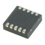
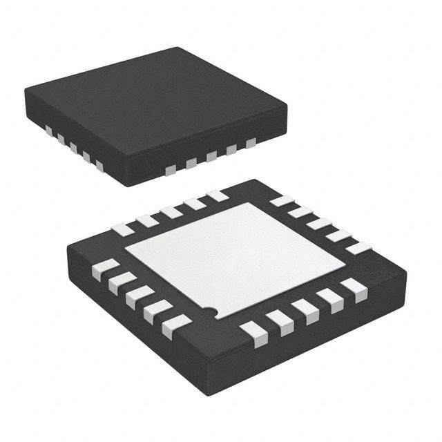
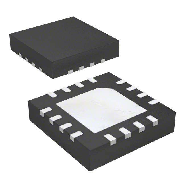
TC1303A/TC1303B/TC1303C/TC1304 Package Types TC1303A,B,C 10-Lead DFN 10-Lead MSOP SHDN2 1 10PGND SHDN2 1 10 PGND VIN2 2 9 LX VIN2 2 9 LX EP V 3 8 V V 3 8 VIN1 OUT2 11 IN1 OUT2 PG 4 7 SHDN1 PG 4 7 SHDN1 AGND 5 6 VFB1/VOUT1 AGND 5 6 VFB1/VOUT1 TC1304 10-Lead DFN 10-Lead MSOP SHDN 1 10PGND SHDN 1 10 PGND VIN2 2 9 LX VIN2 2 9 LX EP VOUT2 3 11 8 VIN1 VOUT2 3 8 VIN1 PG 4 7 AGND PG 4 7 AGND AGND 5 6 VFB1/VOUT1 AGND 5 6 VFB1/VOUT1 DS21949C-page 2 © 2008 Microchip Technology Inc.
TC1303A/TC1303B/TC1303C/TC1304 Functional Block Diagram – TC1303 Undervoltage Lockout UVLO V REF (UVLO) Synchronous Buck Regulator V IN1 PDRV V IN2 L X Control Driver SHDN1 NDRV P GND P P GND GND AGND VOUT1/VFB1 Sense Switcher for A,C PG TC1303A(1),B(2),C(1) options PG Generator with Delay V REF Sense LDO for B,C UVLO V OUT2 LDO SHDN2 A GND Note1: PG open-drain for A,C options 2: PG push-pull output for B option © 2008 Microchip Technology Inc. DS21949C-page 3
TC1303A/TC1303B/TC1303C/TC1304 Functional Block Diagram – TC1304 Undervoltage Lockout UVLO V REF (UVLO) Synchronous Buck Regulator V IN1 PDRV V IN2 L X Control Driver SHDN NDRV P GND P P GND GND AGND VOUT1/VFB1 PG TC1304(Note) Output Voltage PG Generator with Delay A Sequencer ckt. GND V REF UVLO V OUT2 LDO A GND Note: PG open-drain for TC1304 DS21949C-page 4 © 2008 Microchip Technology Inc.
TC1303A/TC1303B/TC1303C/TC1304 Typical Application Circuits TC1303A Fixed-Output Application 10-Lead MSOP 4.7μH V IN 2.7V to 4.2V 8 VIN1 LX 9 VOUT1 4.7μF 2 VIN2 PGND 10 4.7μF 1.5V @ 500mA 7 SHDN1 VOUT1 6 1 SHDN2 VOUT2 3 VOUT2 RPULLUP 4 PG AGND 5 1μF 2.5V @ 300mA Processor RESET TC1303B Adjustable-Output Application 10-Lead DFN 4.7μH Input VIN1 LX VOUT1 4.5VV otolta 5g.e5V 4.7μF VIN2 28 190PGND 4.7ΜF 200kΩ 4.99kΩ 25.010Vm @A SHDN1 V EP OUT1 *COapptiaocniatolr 1.0μF SHDN2 17 11 63 VOUT2 VOUT2 33pF VIN2 PG 4 5 AGND 1ΜF 33.030Vm @A 121kΩ (Note) Processor RESET Note: Connect DFN package exposed pad to A . GND TC1304 Fixed-Output Application 10-Lead MSOP 4.7μH V IN 2.7V to 4.2V 8 VIN1 LX 9 VOUT1 4.7μF 2 VIN2 PGND 10 4.7ΜF 1.2V @ 500mA 7 AGND VOUT1 6 1 SHDN VOUT2 3 VOUT2 RPULLUP 4 PG AGND 5 1μF 2.5V @ 300mA Processor RESET © 2008 Microchip Technology Inc. DS21949C-page 5
TC1303A/TC1303B/TC1303C/TC1304 NOTES: DS21949C-page 6 © 2008 Microchip Technology Inc.
TC1303A/TC1303B/TC1303C/TC1304 1.0 ELECTRICAL † Notice: Stresses above those listed under “Maximum Ratings” may cause permanent damage to the device. This is CHARACTERISTICS a stress rating only and functional operation of the device at those or any other conditions above those indicated in the Absolute Maximum Ratings † operational listings of this specification is not implied. Exposure to maximum rating conditions for extended periods VIN - AGND.......................................................................6.0V may affect device reliability. All Other I/O...............................(A - 0.3V) to (V + 0.3V) GND IN L to P ...............................................-0.3V to (V + 0.3V) X GND IN P to A ..................................................-0.3V to +0.3V GND GND Output Short Circuit Current ................................Continuous Power Dissipation (Note7)..........................Internally Limited Storage temperature.....................................-65°C to +150°C Ambient Temp. with Power Applied................-40°C to +85°C Operating Junction Temperature...................-40°C to +125°C ESD protection on all pins (HBM)....................................... 3kV DC CHARACTERISTICS Electrical Characteristics: V =V =SHDN1,2=3.6V, C =C =4.7µF, C =1µF, L=4.7µH, V (ADJ)=1.8V, IN1 IN2 OUT1 IN OUT2 OUT1 I =100mA, I =0.1mA T =+25°C. Boldface specifications apply over the T range of -40°C to +85°C. OUT1 OUT2 A A Parameters Sym Min Typ Max Units Conditions Input/Output Characteristics Input Voltage V 2.7 — 5.5 V Note1, Note2, Note8 IN Maximum Output Current I 500 — — mA Note1 OUT1_MAX Maximum Output Current I 300 — — mA Note1 OUT2_MAX Shutdown Current I — 0.05 1 µA SHDN1=SHDN2=GND IN_SHDN Combined V and V Current IN1 IN2 TC1303A,B Operating I I — 65.0 110 µA SHDN1=SHDN2=V Q Q IN2 TC1303C, TC1304 Operating I I 70.1 110 I =0mA, I =0mA Q Q OUT1 OUT2 Synchronous Buck I — 38 — µA SHDN1 = V , SHDN2 = GND Q IN LDO I — 46 — µA SHDN1 = GND, SHDN2 = V Q IN2 Shutdown/UVLO/Thermal Shutdown Characteristics SHDN1,SHDN2, SHDN (TC1304) V — — 15 %V V =V =2.7V to 5.5V IL IN IN1 IN2 Logic Input Voltage Low SHDN1,SHDN2, SHDN (TC1304) V 45 — — %V V =V =2.7V to 5.5V IH IN IN1 IN2 Logic Input Voltage High SHDN1,SHDN2, SHDN (TC1304) I -1.0 ±0.01 1.0 µA V =V =2.7V to 5.5V IN IN1 IN2 Input Leakage Current SHDNX=GND SHDNY=V IN Thermal Shutdown T — 165 — °C Note6, Note7 SHD Thermal Shutdown Hysteresis T — 10 — °C SHD-HYS Undervoltage Lockout UVLO 2.4 2.55 2.7 V V Falling IN1 (V and V ) OUT1 OUT2 Undervoltage Lockout Hysteresis UVLO- — 200 — mV HYS Note 1: The Minimum V has to meet two conditions: V ≥ 2.7V and V ≥ V + V V = V or V . IN IN IN RX DROPOUT, RX R1 R2 2: V is the regulator output voltage setting. RX 3: TCV = ((V – V ) * 106)/(V * D ). OUT2 OUT2max OUT2min OUT2 T 4: Regulation is measured at a constant junction temperature using low duty-cycle pulse testing. Load regulation is tested over a load range from 0.1mA to the maximum specified output current. 5: Dropout voltage is defined as the input-to-output voltage differential at which the output voltage drops 2% below its nominal value measured at a 1V differential. 6: The maximum allowable power dissipation is a function of ambient temperature, the maximum allowable junction temperature and the thermal resistance from junction to air. (i.e. T , T , θ ). Exceeding the maximum allowable power A J JA dissipation causes the device to initiate thermal shutdown. 7: The integrated MOSFET switches have an integral diode from the L pin to V , and from L to P . In cases where X IN X GND these diodes are forward-biased, the package power dissipation limits must be adhered to. Thermal protection is not able to limit the junction temperature for these cases. 8: V and V are supplied by the same input source. IN1 IN2 © 2008 Microchip Technology Inc. DS21949C-page 7
TC1303A/TC1303B/TC1303C/TC1304 DC CHARACTERISTICS (CONTINUED) Electrical Characteristics: V =V =SHDN1,2=3.6V, C =C =4.7µF, C =1µF, L=4.7µH, V (ADJ)=1.8V, IN1 IN2 OUT1 IN OUT2 OUT1 I =100mA, I =0.1mA T =+25°C. Boldface specifications apply over the T range of -40°C to +85°C. OUT1 OUT2 A A Parameters Sym Min Typ Max Units Conditions Synchronous Buck Regulator (V ) OUT1 Adjustable Output Voltage Range V 0.8 — 4.5 V OUT1 Adjustable Reference Feedback V 0.78 0.8 0.82 V FB1 Voltage (V ) FB1 Feedback Input Bias Current I — -1.5 — nA VFB1 ( ) IFB1 Output Voltage Tolerance Fixed V -2.5 ±0.3 +2.5 % Note2 OUT1 (V ) OUT1 Line Regulation (V ) V — 0.2 — %/V V =V +1V to 5.5V, OUT1 LINE-REG IN R I = 100mA LOAD Load Regulation (V ) V — 0.2 — % V =V +1.5V, I =100mA to OUT1 LOAD-REG IN R LOAD 500mA (Note1) Dropout Voltage V V – V — 280 — mV I = 500mA, V =3.3V OUT1 IN OUT1 OUT1 OUT1 (Note5) Internal Oscillator Frequency F 1.6 2.0 2.4 MHz OSC Start Up Time T — 0.5 — ms T = 10% to 90% SS R R P-Channel R — 450 — mΩ I =100mA DSon DSon-P P R N-Channel R — 450 — mΩ I =100mA DSon DSon-N N L Pin Leakage Current I -1.0 ±0.01 1.0 μA SHDN = 0V, V = 5.5V, L = 0V, X LX IN X L = 5.5V X Positive Current Limit Threshold +I — 700 — mA LX(MAX) LDO Output (V ) OUT2 Output Voltage Tolerance (V ) V -2.5 ±0.3 +2.5 % Note2 OUT2 OUT2 Temperature Coefficient TCV — 25 — ppm/°C Note3 OUT Line Regulation ∆V / -0.2 ±0.02 +0.2 %/V (V +1V) ≤ V ≤ 5.5V OUT2 R IN ∆V IN Load Regulation, V ≥ 2.5V ∆V / -0.75 -0.08 +0.75 % I = 0.1mA to 300mA(Note4) OUT2 OUT2 OUT2 I OUT2 Load Regulation, V < 2.5V ∆V / -0.9 -0.18 +0.9 % I = 0.1mA to 300mA(Note4) OUT2 OUT2 OUT2 I OUT2 Dropout Voltage V > 2.5V V – V — 137 300 mV I = 200mA (Note5) OUT2 IN OUT2 OUT2 205 500 I =300mA OUT2 Power Supply Rejection Ratio PSRR — 62 — dB f ≤ 100Hz, I = I = 50mA, OUT1 OUT2 C = 0µF IN Output Noise eN — 1.8 — µV/(Hz)½ f ≤ 1kHz, I =50mA, OUT2 SHDN1=GND Note 1: The Minimum V has to meet two conditions: V ≥ 2.7V and V ≥ V + V V = V or V . IN IN IN RX DROPOUT, RX R1 R2 2: V is the regulator output voltage setting. RX 3: TCV = ((V – V ) * 106)/(V * D ). OUT2 OUT2max OUT2min OUT2 T 4: Regulation is measured at a constant junction temperature using low duty-cycle pulse testing. Load regulation is tested over a load range from 0.1mA to the maximum specified output current. 5: Dropout voltage is defined as the input-to-output voltage differential at which the output voltage drops 2% below its nominal value measured at a 1V differential. 6: The maximum allowable power dissipation is a function of ambient temperature, the maximum allowable junction temperature and the thermal resistance from junction to air. (i.e. T , T , θ ). Exceeding the maximum allowable power A J JA dissipation causes the device to initiate thermal shutdown. 7: The integrated MOSFET switches have an integral diode from the L pin to V , and from L to P . In cases where X IN X GND these diodes are forward-biased, the package power dissipation limits must be adhered to. Thermal protection is not able to limit the junction temperature for these cases. 8: V and V are supplied by the same input source. IN1 IN2 DS21949C-page 8 © 2008 Microchip Technology Inc.
TC1303A/TC1303B/TC1303C/TC1304 DC CHARACTERISTICS (CONTINUED) Electrical Characteristics: V =V =SHDN1,2=3.6V, C =C =4.7µF, C =1µF, L=4.7µH, V (ADJ)=1.8V, IN1 IN2 OUT1 IN OUT2 OUT1 I =100mA, I =0.1mA T =+25°C. Boldface specifications apply over the T range of -40°C to +85°C. OUT1 OUT2 A A Parameters Sym Min Typ Max Units Conditions Output Short Circuit Current I — 240 — mA R ≤ 1Ω OUTsc2 LOAD2 (Average) Wake-Up Time (From SHDN2 t — 31 100 µs I = I = 50mA WK OUT1 OUT2 mode), (V ) OUT2 Settling Time (From SHDN2 t — 100 — µs I = I = 50mA S OUT1 OUT2 mode), (V ) OUT2 Power-Good (PG) Voltage Range PG V 1.0 — 5.5 V T = 0°C to +70°C PG A 1.2 5.5 T = -40°C to +85°C A V ≤ 2.7 I = 100µA IN SINK PG Threshold High V — 94 96 % of On Rising V or V TH_H OUT1 OUT2 (V or V ) V V =V or V OUT1 OUT2 OUTX OUTX OUT1 OUT2 PG Threshold Low V 89 92 — % of On Falling V or V TH_L OUT1 OUT2 (V or V ) V V =V or V OUT1 OUT2 OUTX OUTX OUT1 OUT2 PG Threshold Hysteresis V — 2 — % of V =V or V TH_HYS OUTX OUT1 OUT2 (V and V ) V OUT1 OUT2 OUTX PG Threshold Tempco ΔV /ΔT — 30 — ppm/°C TH PG Delay t — 165 — µs V or V =(V + 100mV) RPD OUT1 OUT2 TH to (V - 100mV) TH PG Active Time-out Period t 140 262 560 ms V orV =V -100mV RPU OUT1 OUT2 TH toV 100mV, TH+ I = 1.2mA SINK PG Output Voltage Low PG_V — — 0.2 V V or V =V -100mV OL OUT1 OUT2 TH , I = 1.2mA V >2.7V PG IN2 I = 100µA, 1.0V<V < 2.7V PG IN2 PG Output Voltage High PG_V 0.9*V — — V V or V =V + 100mV OH OUT2 OUT1 OUT2 TH (TC1303B only) V ≥ 1.8V, I =-500µA OUT2 PG V < 1.8V,I =-300µA OUT2 PG Note 1: The Minimum V has to meet two conditions: V ≥ 2.7V and V ≥ V + V V = V or V . IN IN IN RX DROPOUT, RX R1 R2 2: V is the regulator output voltage setting. RX 3: TCV = ((V – V ) * 106)/(V * D ). OUT2 OUT2max OUT2min OUT2 T 4: Regulation is measured at a constant junction temperature using low duty-cycle pulse testing. Load regulation is tested over a load range from 0.1mA to the maximum specified output current. 5: Dropout voltage is defined as the input-to-output voltage differential at which the output voltage drops 2% below its nominal value measured at a 1V differential. 6: The maximum allowable power dissipation is a function of ambient temperature, the maximum allowable junction temperature and the thermal resistance from junction to air. (i.e. T , T , θ ). Exceeding the maximum allowable power A J JA dissipation causes the device to initiate thermal shutdown. 7: The integrated MOSFET switches have an integral diode from the L pin to V , and from L to P . In cases where X IN X GND these diodes are forward-biased, the package power dissipation limits must be adhered to. Thermal protection is not able to limit the junction temperature for these cases. 8: V and V are supplied by the same input source. IN1 IN2 © 2008 Microchip Technology Inc. DS21949C-page 9
TC1303A/TC1303B/TC1303C/TC1304 TEMPERATURE SPECIFICATIONS Electrical Specifications: Unless otherwise indicated, all limits are specified for: V = +2.7V to +5.5V IN Parameters Sym Min Typ Max Units Conditions Temperature Ranges Operating Junction Temperature T -40 — +125 °C Steady state J Range Storage Temperature Range T -65 — +150 °C A Maximum Junction Temperature T — — +150 °C Transient J Thermal Package Resistances Thermal Resistance, 10L-DFN θ — 41 — °C/W Typical 4-layer Board with JA Internal Ground Plane and 2 Vias in Thermal Pad Thermal Resistance, 10L-MSOP θ — 113 — °C/W Typical 4-layer Board with JA Internal Ground Plane DS21949C-page 10 © 2008 Microchip Technology Inc.
TC1303A/TC1303B/TC1303C/TC1304 2.0 TYPICAL PERFORMANCE CURVES Note: The graphs and tables provided following this note are a statistical summary based on a limited number of samples and are provided for informational purposes only. The performance characteristics listed herein are not tested or guaranteed. In some graphs or tables, the data presented may be outside the specified operating range (e.g., outside specified power supply range) and therefore outside the warranted range. Note: Unless otherwise indicated, V = V =SHDN1,2 =3.6V, C =C =4.7µF, C =1µF, L=4.7µH, IN1 IN2 OUT1 IN OUT2 V (ADJ)=1.8V, T =+25°C. Boldface specifications apply over the T range of -40°C to +85°C. T =+25°C. Adjustable- or fixed- OUT1 A A A output voltage options can be used to generate the Typical Performance Characteristics. 80 55 O (µA) 76 IOUT1 = IOUT2 = 0 mA SSHHDDNN12 == VVIINN22 50 IOUT2 = 0 mA VIN = 5.5V LD VIN = 5.5V A) er and 6782 VIN = 4.2V LDO (µ 4405 VIN = 3.6V VIN = 4.2V I SwitchQ 64 VIN = 3.6V I Q 35 SSHHDDNN12 == AVIGNN2D 60 30 -40 -25 -10 5 20 35 50 65 80 95 110125 -40 -25 -10 5 20 35 50 65 80 95 110125 Ambient Temperature (°C) Ambient Temperature (°C) FIGURE 2-1: I Switcher and LDO FIGURE 2-4: I LDO Current vs. Ambient Q Q Current vs. Ambient Temperature (TC1303A,B). Temperature. DO (µA) 777468 SSHHDDNN12 == VVIINN22 VIN = 5.5V y (%) 108990505 IOUT1 = 100 mA SSHHDDNN12 == VAIGNN2D Switcher and L 677802 VIN = 4V.2INV = 3.6V V EfficiencOUT1 6677805050 IIOOUUTT11 == 255000 mmAA Q 55 I 66 50 -40 -25 -10 5 20 35 50 65 80 95 110125 2.7 3.05 3.4 3.75 4.1 4.45 4.8 5.15 5.5 Ambient Temperature (°C) Input Voltage (V) FIGURE 2-2: I Switcher and LDO FIGURE 2-5: V Output Efficiency vs. Q OUT1 Current vs. Ambient Temperature Input Voltage (V = 1.2V). OUT1 (TC1303C, TC1304). 55 SHDN1 = VIN2 100 50 IOUT1 = 0 mA VIN = 5.5V SHDN2 = AGND %) 95 SSHHDDNN12 == VAIGNN2D µA) cy( 90 her ( 45 cien 85 I SwitcQ 3450 VIN = 4.2V VIN = 3.6V V EffiOUT1 7850 VIN1 = 4.2V VIN1 = 3.0VVIN1 = 3.6V 30 70 -40 -25 -10 5 20 35 50 65 80 95 110125 0.005 0.104 0.203 0.302 0.401 0.5 Ambient Temperature (°C) IOUT1 (A) FIGURE 2-3: I Switcher Current vs. FIGURE 2-6: V Output Efficiency vs. Q OUT1 Ambient Temperature. I (V = 1.2V). OUT1 OUT1 © 2008 Microchip Technology Inc. DS21949C-page 11
TC1303A/TC1303B/TC1303C/TC1304 Note: Unless otherwise indicated, V = V =SHDN1,2 =3.6V, C =C =4.7µF, C =1µF, L=4.7µH, IN1 IN2 OUT1 IN OUT2 V (ADJ)=1.8V, T =+25°C. Boldface specifications apply over the T range of -40°C to +85°C. T =+25°C. Adjustable- or fixed- OUT1 A A A output voltage options can be used to generate the Typical Performance Characteristics. 100 SHDN1 = VIN2 100 VIN1 = 3.6V y(%) 9905 IOUT1 = 100 mA SHDN2 = AGND y (%) 9905 EfficiencOUT1 77880505 IOUT1 = 250 mA IOUT1 = 500 mA EfficiencOUT1 77880505 VINV1 I=N1 5 =.5 4V.2V SSHHDDNN12 == VAIGNN2D V V 65 65 60 60 2.7 3.05 3.4 3.75 4.1 4.45 4.8 5.15 5.5 0.005 0.104 0.203 0.302 0.401 0.5 Input Voltage (V) IOUT1 (A) FIGURE 2-7: V Output Efficiency vs. FIGURE 2-10: V Output Efficiency vs. OUT1 OUT1 Input Voltage (V = 1.8V). I (V = 3.3V). OUT1 OUT1 OUT1 100 1.21 SHDN1 = VIN2 SHDN1 = VIN2 y(%) 95 VIN = 3.0V SHDN2 = AGND 1.206 VIN1 = 3.6V SHDN2 = AGND nc 90 V) 1.202 Efficie 85 VIN = 4.2V V (OUT1 1.198 UT1 VO 80 VIN = 3.6V 1.194 75 1.19 0.005 0.104 0.203 0.302 0.401 0.5 0.005 0.104 0.203 0.302 0.401 0.5 I (A) I (A) OUT1 OUT1 FIGURE 2-8: V Output Efficiency vs. FIGURE 2-11: V vs. I OUT1 OUT1 OUT1 I (V = 1.8V). (V = 1.2V). OUT1 OUT1 OUT1 100 1.82 SHDN1 = VIN2 SHDN1 = VIN2 %) 96 IOUT1 = 100 mA SHDN2 = AGND 1.815 VIN1 = 3.6V SHDN2 = AGND y ( 1.81 nc 92 V) Efficie 88 IOUT1 = 250 mA V (OUT1 1.805 UT1 IOUT1 = 500 mA 1.8 VO 84 1.795 80 1.79 3.60 3.92 4.23 4.55 4.87 5.18 5.50 0.005 0.104 0.203 0.302 0.401 0.5 Input Voltage (V) IOUT1 (A) FIGURE 2-9: V Output Efficiency vs. FIGURE 2-12: V vs. I OUT1 OUT1 OUT1 Input Voltage (V = 3.3V). (V = 1.8V). OUT1 OUT1 DS21949C-page 12 © 2008 Microchip Technology Inc.
TC1303A/TC1303B/TC1303C/TC1304 Note: Unless otherwise indicated, V = V =SHDN1,2 =3.6V, C =C =4.7µF, C =1µF, L=4.7µH, IN1 IN2 OUT1 IN OUT2 V (ADJ)=1.8V, T =+25°C. Boldface specifications apply over the T range of -40°C to +85°C. T =+25°C. Adjustable- or fixed- OUT1 A A A output voltage options can be used to generate the Typical Performance Characteristics. 3.4 0.820 SHDN1 = VIN2 SHDN1 = VIN2 3.36 SHDN2 = AGND V) 0.815 SHDN2 = AGND VIN1 = 4.2V e ( VIN1 = 3.6V g 0.810 V (V)OUT1 33..2382 FB VoltaUT1 00..880005 3.24 VO 0.795 3.2 0.790 0.005 0.104 0.203 0.302 0.401 0.5 40 25 10 5 20 35 50 65 80 95 10 25 - - - 1 1 IOUT1 (A) Ambient Temperature (°C) FIGURE 2-13: V vs. I FIGURE 2-16: V Adjustable Feedback OUT1 OUT1 OUT1 (V = 3.3V). Voltage vs. Ambient Temperature. OUT1 2.20 0.6 SHDN1 = VIN2 (cid:2)) SHDN1 = VIN2 MHz) 2.15 SHDN2 = AGND nce ( 0.55 TA = 25 °C SHDN2 = AGND uency ( 22..0150 Resista 00.4.55 V FreqOUT1 12..9050 Switch UT1 00.3.45 N-CPh-Cahnannenlel O V 1.90 0.3 2.7 3.1 3.5 3.9 4.3 4.7 5.1 5.5 3.3 3.5 3.7 3.9 4.1 4.3 4.5 4.7 4.9 5.1 5.3 5.5 Input Voltage (V) Input Voltage (V) FIGURE 2-14: V Switching Frequency FIGURE 2-17: V Switch Resistance OUT1 OUT1 vs. Input Voltage. vs. Input Voltage. MHz) 12..9080 SSHHDDNN12 == VAIGNN2D nce ((cid:2)) 0.06.56 VIN1 = 3.6V SSHHDDNN12 == VAIGNN2D ncy ( 1.96 sista 0.05.55 P-Channel ue Re N-Channel V FreqOUT1 11..9924 Switch UT100..034.554 O 1.90 V 0.3 0 5 0 5 0 5 0 5 0 5 0 5 4 2 1 2 3 5 6 8 9 1 2 -40 -25 -10 5 20 35 50 65 80 95 110125 - - - 1 1 Ambient Temperature (°C) Ambient Temperature (°C) FIGURE 2-15: V Switching Frequency FIGURE 2-18: V Switch Resistance OUT1 OUT1 vs. Ambient Temperature. vs. Ambient Temperature. © 2008 Microchip Technology Inc. DS21949C-page 13
TC1303A/TC1303B/TC1303C/TC1304 Note: Unless otherwise indicated, V = V =SHDN1,2 =3.6V, C =C =4.7µF, C =1µF, L=4.7µH, IN1 IN2 OUT1 IN OUT2 V (ADJ)=1.8V, T =+25°C. Boldface specifications apply over the T range of -40°C to +85°C. T =+25°C. Adjustable- or fixed- OUT1 A A A output voltage options can be used to generate the Typical Performance Characteristics. 0.4 1.492 IOUT2 = 150 mA V Dropout Voltage (V)OUT1 000...00123..55523 SSHHDDNN12 == VAIGNN2D IOUVT1O U=T 15 0=0 3 m.3AV V Output Voltage(V)OUT2 111...1444.88844689 TTTAAA=== + -+ 42 8055°°CC°C SSHHDDNN12 == AVIGNN2D 0.1 1.482 0 5 0 5 0 5 0 5 0 5 0 5 4 2 1 2 3 5 6 8 9 1 2 2.7 3.05 3.4 3.75 4.1 4.45 4.8 5.15 5.5 - - - 1 1 Ambient Temperature (°C) Input Voltage (V) FIGURE 2-19: V Dropout Voltage vs. FIGURE 2-22: V Output Voltage vs. OUT1 OUT2 Ambient Temperature. Input Voltage (V = 1.5V). OUT2 1.802 ge (V) 1.800 IOUT2 = 150 mA TA= + 85°C SSHHDDNN12 == AVIGNN2D a olt 1.798 ut V TA= + 25°C utp 1.796 O UT2 1.794 TA= - 40°C O V 1.792 2.7 3.05 3.4 3.75 4.1 4.45 4.8 5.15 5.5 Input Voltage (V) FIGURE 2-20: V and V Heavy FIGURE 2-23: V Output Voltage vs. OUT1 OUT2 OUT2 Load Switching Waveforms vs. Time. Input Voltage (V = 1.8V). OUT2 2.508 e (V) 2.506 IOUT2 = 150 mA SSHHDDNN12 == AVIGNN2D oltag 2.504 TA= + 85°C V ut 2.502 TA= + 25°C p Out 2.500 V OUT2 2.498 TA= - 40°C 2.496 3.3 3.5 3.7 3.9 4.1 4.3 4.5 4.7 4.9 5.1 5.3 5.5 Input Voltage (V) FIGURE 2-21: V and V Light FIGURE 2-24: V Output Voltage vs. OUT1 OUT2 OUT2 Load Switching Waveforms vs. Time. Input Voltage (V = 2.5V). OUT2 DS21949C-page 14 © 2008 Microchip Technology Inc.
TC1303A/TC1303B/TC1303C/TC1304 Note: Unless otherwise indicated, V = V =SHDN1,2 =3.6V, C =C =4.7µF, C =1µF, L=4.7µH, IN1 IN2 OUT1 IN OUT2 V (ADJ)=1.8V, T =+25°C. Boldface specifications apply over the T range of -40°C to +85°C. T =+25°C. Adjustable- or fixed- OUT1 A A A output voltage options can be used to generate the Typical Performance Characteristics. 3.298 0.005 SHDN1 = AGND oltage (V) 33..229967 IOUT2 = 150 mA TA = + 85°C SSHHDDNN12 == AVIGNN2D ation (%/V) --000...000010005 VOUT2= 3.3V SHDN2 = VIN2 IOUT2 = 100 µA put V 3.295 TA = + 25°C Regul -0.015 VOUT2 = 2.5V Out 3.294 ne -0.020 V OUT2 3.293 TA = - 40°C LiOUT2 --00..003205 VOUT2 = 1.5V V 3.292 -0.035 3.60 3.92 4.23 4.55 4.87 5.18 5.50 -40 -25 -10 5 20 35 50 65 80 95 110125 Input Voltage (V) Ambient Temperature (°C) FIGURE 2-25: V Output Voltage vs. FIGURE 2-28: V Line Regulation vs. OUT2 OUT2 Input Voltage (V = 3.3V). Ambient Temperature. OUT2 0.30 0.1 V) SHDN1 = AGND %) VIN2 = 3.6V SHDN1 = AGND e ( 0.25 SHDN2 = VIN2 n ( 0.0 VOUT2 = 3.3V SHDN2 = VIN2 pout Voltag 00..1250 IOIOUUTT22 = = 3 20000 m mAA d Regulatio --00..21 Dro Loa VOUT2= 2.6V V OUT2 0.10 V OUT2 -0.3 VOUT2 = 1.5V 0.05 -0.4 0 5 0 5 0 5 0 5 0 5 0 5 0 5 0 5 0 5 0 5 0 5 0 5 4 2 1 2 3 5 6 8 9 1 2 4 2 1 2 3 5 6 8 9 1 2 - - - 1 1 - - - 1 1 Ambient Temperature (°C) Ambient Temperature (°C) FIGURE 2-26: V Dropout Voltage vs. FIGURE 2-29: V Load Regulation vs. OUT2 OUT2 Ambient Temperature (V = 2.5V). Ambient Temperature. OUT2 0.3 350 age (V) SSHHDDNN12 == AVIGNN2D me (ms) 325 VIN = 3.6V SSHHDDNN12 == VVIINN22 Volt 0.2 IOUT2 = 300 mA y Ti 300 out Dela 275 DropOUT2 0.1 IOUT2 = 200 mA G Active 222550 V P 0.0 200 -40 -25 -10 5 20 35 50 65 80 95 110125 -40 -25 -10 5 20 35 50 65 80 95 110125 Ambient Temperature (°C) Ambient temperature (°C) FIGURE 2-27: V Dropout Voltage vs. FIGURE 2-30: PG Active Delay Time-out OUT2 Ambient Temperature (V = 3.3V). vs. Ambient Temperature. OUT2 © 2008 Microchip Technology Inc. DS21949C-page 15
TC1303A/TC1303B/TC1303C/TC1304 Note: Unless otherwise indicated, V = V =SHDN1,2 =3.6V, C =C =4.7µF, C =1µF, L=4.7µH, IN1 IN2 OUT1 IN OUT2 V (ADJ)=1.8V, T =+25°C. Boldface specifications apply over the T range of -40°C to +85°C. T =+25°C. Adjustable- or fixed- OUT1 A A A output voltage options can be used to generate the Typical Performance Characteristics. 96 0 )OUT2 95 VIN = 3.6V SSHHDDNN12 == VVIINN22 -10 SVOHUDT2N =1 1=. 5GVND COUT2 = 1.0 µF % of V 94 PG Threshold Hi R (dB) --3200 ICOIUNT =2 =0 3µ0F mA d ( 93 SR -40 ol P hresh 92 PG Threshold Low V OUT2 --6500 COUT2 = 4.7 µF T 91 G -70 P 90 -80 -40 -25 -10 5 20 35 50 65 80 95 110125 0.01 0.1 1 10 100 1000 Ambient Temperature (°C) Frequency (kHz) FIGURE 2-31: PG Threshold Voltage vs. FIGURE 2-34: V Power Supply Ripple OUT2 Ambient Temperature. Rejection vs. Frequency. 0.02 10 VIN = 3.6V SHDN1 = VIN2 SHDN1 = AGND 0.018 SHDN2 = VIN2 z) SHDN2 = VIN2 H (cid:2) V (V)OL 0.016 IOL = 1.2 mA se (μV/ 1 G 0.014 oi P 0.012 NOUT2 0.1 VIN = 3.6V V VOUT2 = 2.5V 0.01 IOUT2 = 50 mA 0.01 0 5 0 5 0 5 0 5 0 5 0 5 -4 -2 -1 2 3 5 6 8 9 11 12 0.01 0.1 1 10 100 1000 10000 Ambient Temperature (°C) Frequency (kHz) FIGURE 2-32: PG Output Voltage Level FIGURE 2-35: V Noise vs. Frequency. OUT2 Low vs. Ambient Temperature. 3.0 VOUT2 = 2.8V 2.5 VOUT2 = 2.5V V) 2.0 (H O 1.5 V G VOUT2 = 1.5V P 1.0 0.5 VIN = 3.6V SHDN1 = VIN2 IOH = 500 µA SHDN2 = VIN2 0.0 -40 -25 -10 5 20 35 50 65 80 95 110125 Ambient Temperature (°C) FIGURE 2-33: PG Output Voltage Level FIGURE 2-36: V Load Step Response OUT1 High vs. Ambient Temperature. vs. Time. DS21949C-page 16 © 2008 Microchip Technology Inc.
TC1303A/TC1303B/TC1303C/TC1304 Note: Unless otherwise indicated, V = V =SHDN1,2 =3.6V, C =C =4.7µF, C =1µF, L=4.7µH, IN1 IN2 OUT1 IN OUT2 V (ADJ)=1.8V, T =+25°C. Boldface specifications apply over the T range of -40°C to +85°C. T =+25°C. Adjustable- or fixed- OUT1 A A A output voltage options can be used to generate the Typical Performance Characteristics. FIGURE 2-37: V Load Step Response FIGURE 2-40: V and V Shutdown OUT2 OUT1 OUT2 vs. Time. Waveforms. FIGURE 2-38: V and V Line Step FIGURE 2-41: Power-Good Output Timing. OUT1 OUT2 Response vs. Time. FIGURE 2-39: V and V Start-up FIGURE 2-42: Start-up Waveforms OUT1 OUT2 Waveforms. (TC1304). © 2008 Microchip Technology Inc. DS21949C-page 17
TC1303A/TC1303B/TC1303C/TC1304 Note: Unless otherwise indicated, V = V =SHDN1,2 =3.6V, C =C =4.7µF, C =1µF, L=4.7µH, IN1 IN2 OUT1 IN OUT2 V (ADJ)=1.8V, T =+25°C. Boldface specifications apply over the T range of -40°C to +85°C. T =+25°C. Adjustable- or fixed- OUT1 A A A output voltage options can be used to generate the Typical Performance Characteristics. FIGURE 2-43: Shutdown Waveforms (TC1304). DS21949C-page 18 © 2008 Microchip Technology Inc.
TC1303A/TC1303B/TC1303C/TC1304 3.0 PIN DESCRIPTIONS The descriptions of the pins are listed in Table3-1. TABLE 3-1: PIN FUNCTION TABLE Symbol Pin No. TC1303 TC1304 Description MSOP, DFN MSOP, DFN 1 SHDN2 — Active Low Shutdown Input for LDO Output Pin 1 — SHDN Active Low Shutdown Input both Buck Regulator Output and LDO Output. Initiates sequencing up and down 2 V V Analog Input Supply Voltage Pin IN2 IN2 3 V V LDO Output Voltage Pin OUT2 OUT2 4 PG PG Power-Good Output Pin 5 A A Analog Ground Pin GND GND 6 V /V V /V Buck Feedback Voltage (Adjustable Version) / Buck Output Voltage FB OUT1 FB OUT1 (Fixed Version) Pin 7 SHDN1 — Active Low Shutdown Input for Buck Regulator Output Pin 7 — A Analog Ground Pin GND 8 V V Buck Regulator Input Voltage Pin IN1 IN1 9 L L Buck Inductor Output Pin X X 10 P P Power Ground Pin GND GND 11 EP EP Exposed Pad - For the DFN package, the center exposed pad is a thermal path to remove heat from the device. Electrically this pad is at ground potential and should be connected to A . GND 3.1 TC1303 LDO Shutdown Input Pin 3.4 LDO Output Voltage Pin (V ) OUT2 (SHDN2) V is a regulated LDO output voltage pin. Connect OUT2 SHDN2 is a logic-level input used to turn the LDO a 1µF or larger capacitor to VOUT2 and AGND for proper Regulator on and off. A logic-high (> 45% of V ), will operation. IN enable the regulator output. A logic-low (< 15% of V ) IN 3.5 Power-Good Output Pin (PG) will ensure that the output is turned off. PG is an output level indicating that V (LDO) is OUT2 3.2 TC1304 Shutdown Input Pin within 94% of regulation. The PG output is configured (SHDN) as a push-pull for the TC1303B and open-drain output for the TC1303A, TC1303C and TC1304. SHDN is a logic-level input used to initiate the sequencing of the LDO output, then the buck regulator 3.6 Analog Ground Pin (A ) output. A logic-high (> 45% of V ), will enable the GND IN regulator outputs. A logic-low (< 15% of VIN) will ensure AGND is the analog ground connection. Tie AGND to the that the outputs are turned off. analog portion of the ground plane (A ). See the GND physical layout information in Section5.0 “Application 3.3 LDO Input Voltage Pin (V ) Circuits/Issues” for grounding recommendations. IN2 V is a LDO power input supply pin. Connect variable 3.7 Buck Regulator Output Sense Pin IN2 input voltage source to VIN2. Connect VIN1 and VIN2 (VFB/VOUT1) together with board traces as short as possible. V IN2 provides the input voltage for the LDO. An additional For VOUT1 adjustable-output voltage options, connect capacitor can be added to lower the LDO regulator the center of the output voltage divider to the VFB pin. input ripple voltage. For fixed-output voltage options, connect the output of the buck regulator to this pin (V ). OUT1 © 2008 Microchip Technology Inc. DS21949C-page 19
TC1303A/TC1303B/TC1303C/TC1304 3.8 Buck Regulator Shutdown Input 3.11 Power Ground Pin (P ) GND Pin (SHDN1) Connect all large-signal level ground returns to P . GND SHDN1 is a logic-level input used to turn the buck These large-signal, level ground traces should have a regulator on and off. A logic-high (> 45% of V ), will small loop area and length to prevent coupling of IN enable the regulator output. A logic-low (< 15% of V ) switching noise to sensitive traces. Please see the IN will ensure that the output is turned off. physical layout information supplied in Section5.0 “Application Circuits/Issues” for grounding 3.9 Buck Regulator Input Voltage Pin recommendations. (V ) IN1 3.12 Exposed Pad (EP) V is the buck regulator power input supply pin. IN1 For the DFN package, connect the EP to A , with Connect a variable input voltage source to VIN1. GND vias into the A plane. Connect V and V together with board traces as GND IN1 IN2 short as possible. 3.10 Buck Inductor Output Pin (L ) X Connect L directly to the buck inductor. This pin X carries large signal-level current; all connections should be made as short as possible. DS21949C-page 20 © 2008 Microchip Technology Inc.
TC1303A/TC1303B/TC1303C/TC1304 4.0 DETAILED DESCRIPTION 4.2.1 FIXED-FREQUENCY PWM MODE While operating in Pulse Width Modulation (PWM) 4.1 Device Overview mode, the TC1303/TC1304 buck regulator switches at a fixed, 2.0MHz frequency. The PWM mode is suited The TC1303/TC1304 combines a 500mA for higher load current operation, maintaining low synchronous buck regulator with a 300mA LDO and a output noise and high conversion efficiency. PFM-to- power-good output. This unique combination provides PWM mode transition is initiated for any of the following a small, low-cost solution for applications that require conditions: two or more voltage rails. The buck regulator can deliver high-output current over a wide range of input- • Continuous inductor current is sensed to-output voltage ratios while maintaining high • Inductor peak current exceeds 100mA efficiency. This is typically used for the lower-voltage, • The buck regulator output voltage has dropped high-current processor core. The LDO is a minimal out of regulation (step load has occurred) parts-count solution (single-output capacitor), providing The typical PFM-to-PWM threshold is 80mA. a regulated voltage for an auxiliary rail. The typical LDO dropout voltage (137mV @ 200mA) allows the use of 4.2.2 PFM MODE very low input-to-output LDO differential voltages, PFM mode is entered when the output load on the buck minimizing the power loss internal to the LDO pass regulator is very light. Once detected, the converter transistor. A power-good output is provided, indicating enters the PFM mode automatically and begins to skip that the buck regulator output, the LDO output or both pulses to minimize unnecessary quiescent current outputs are in regulation. Additional features include draw by reducing the number of switching cycles per independent shutdown inputs (TC1303), UVLO, output second. The typical quiescent current for the switching voltage sequencing (TC1304), overcurrent and regulator is less than 35µA. The transition from PWM overtemperature shutdown. to PFM mode occurs when discontinuous inductor current is sensed or the peak inductor current is less 4.2 Synchronous Buck Regulator than 60mA (typical). The typical PWM to PFM mode The synchronous buck regulator is capable of threshold is 30mA. For low input-to-output differential supplying a 500mA continuous output current over a voltages, the PWM-to-PFM mode threshold can be low wide range of input and output voltages. The output due to the lack of ripple current. It is recommended that voltage range is from 0.8V (minimum) to 4.5V VIN1 be one volt greater than VOUT1 for PWM-to-PFM (maximum). The regulator operates in three different transitions. modes, automatically selecting the most efficient mode 4.3 Low Drop Out Regulator (LDO) of operation. During heavy load conditions, the TC1303/TC1304 buck converter operates at a high, The LDO output is a 300mA low-dropout linear fixed frequency (2.0MHz) using current mode control. regulator that provides a regulated output voltage with This minimizes output ripple and noise (less than 8mV a single 1µF external capacitor. The output voltage is peak-to-peak ripple) while maintaining high efficiency available in fixed options only, ranging from 1.5V to (typically > 90%). For standby or light load applications, 3.3V. The LDO is stable using ceramic output the buck regulator will automatically switch to a power- capacitors that inherently provide lower output noise saving Pulse Frequency Modulation (PFM) mode. This and reduce the size and cost of the regulator solution. minimizes the quiescent current draw on the battery, The quiescent current consumed by the LDO output is while keeping the buck output voltage in regulation. typically less than 40µA, with a typical dropout voltage The typical buck PFM mode current is 38µA. The buck of 137mV at 200mA. While operating in Dropout regulator is capable of operating at 100% duty cycle, mode, the LDO quiescent current will increase, minimizing the voltage drop from input-to-output for minimizing the necessary voltage differential needed wide input, battery-powered applications. For fixed- for the LDO output to maintain regulation. The LDO output voltage applications, the feedback divider and output is protected against overcurrent and control loop compensation components are integrated, overtemperature conditions. eliminating the need for external components. The buck regulator output is protected against overcurrent, short circuit and overtemperature. While shut down, the synchronous buck N-channel and P-channel switches are off, so the L pin is in a high-impedance state (this X allows for connecting a source on the output of the buck regulator as long as its voltage does not exceed the input voltage). © 2008 Microchip Technology Inc. DS21949C-page 21
TC1303A/TC1303B/TC1303C/TC1304 4.4 Power-Good 4.5 Power Good Output Options A Power-Good (PG) output signal is generated based There are three monitoring options for the TC1303 off of the buck regulator output voltage (V ), the family. OUT1 LDO output voltage (V ) or the combination of both OUT2 For the TC1303A, only the buck regulator output outputs. A fixed delay time of approximately 262ms is voltage (V ) is monitored. The PG output signal OUT1 generated once the monitored output voltage is above depends only on V . OUT1 the power-good threshold (typically 94% of V ). As OUTX the monitored output voltage falls out of regulation, the For the TC1303B, only the LDO output voltage (VOUT2) falling PG threshold is typically 92% of the output is monitored. The PG output signal depends only on voltage. The PG output signal is pulled up to the output VOUT2. voltage, indicating that power is good and pulled low, For the TC1303C and TC1304, both the buck regulator indicating that the output is out of regulation. The output voltage and LDO output voltage are monitored. typical quiescent current draw for power-good circuitry If either one of the outputs fall out of regulation, the PG is less than 10µA. will be low. Only if both V and V are within the OUT1 OUT2 PG voltage threshold limits will the PG output be high. If the monitored output voltage falls below the power- good threshold, the power-good output will transition to For the TC1303A,C and TC1304, the PG output pin is the Low state. The power-good circuitry has a 165µs open drain and can be pulled up to any level within the delay when detecting a falling output voltage. This given absolute maximum ratings (A - 0.3V) to (V GND IN helps to increase the noise immunity of the power-good + 0.3V). output, avoiding false triggering of the PG signal during line and load transients. TABLE 4-1: PG AVAILABLE OPTIONS PG PG Output Part Output PG Output VTH_H Buck Number LDO Type (V ) V OUT1 (V ) OUT1 OUT2 or V OUT2 TC1303A Yes No Open-Drain t RPU TC1303B No Yes Push-Pull (V ) V OUT2 OH t TC1303C Yes Yes Open-Drain RPD TC1304 Yes Yes Open-Drain PG V OL FIGURE 4-1: Power-Good Timing. DS21949C-page 22 © 2008 Microchip Technology Inc.
TC1303A/TC1303B/TC1303C/TC1304 4.6 TC1304 Sequencing the turn on of the Buck Regulator output (V ) until OUT1 the LDO output is in regulation. During power-down, The TC1304 device features an integrated sequencing the sequencing circuit will turn off the Buck Regulator option. A sequencing circuit using only the SHDN input, output prior to turning off LDO output. (Pin1), will turn on the LDO output (V ) and delay OUT2 SHDN VOUT2 + 160µs Delay* Enable – To PG Delay CKT. 92% of V OUT2 + 160µs Delay* V OUT1 Enable – 92% of V OUT1 * 160µs delay on trailing edge FIGURE 4-2: TC1304 Sequencing Circuit. 4.7 Soft Start TC1304 Both outputs of the TC1303/TC1304 are controlled Power Up Timing From SHDN during start-up. Less than 1% of V or V OUT1 OUT2 overshoot is observed during start-up from V rising V /V IN IN1 IN2 above the UVLO voltage or either SHDN1 or SHDN2 being enabled. SHDN 4.8 Overtemperature Protection 500µs The TC1303/TC1304 has an integrated overtempera- ture protection circuit that monitors the device junction V OUT1 temperature and shuts the device off if the junction tWK + tS temperature exceeds the typical 165°C threshold. If the overtemperature threshold is reached, the soft start is V reset so that, once the junction temperature cools to OUT2 approximately 155°C, the device will automatically 300ms restart. Power Good FIGURE 4-3: TC1304 Power-up Timing from SHDN. © 2008 Microchip Technology Inc. DS21949C-page 23
TC1303A/TC1303B/TC1303C/TC1304 NOTES: DS21949C-page 24 © 2008 Microchip Technology Inc.
TC1303A/TC1303B/TC1303C/TC1304 5.0 APPLICATION CIRCUITS/ An additional V capacitor can be added to reduce IN2 ISSUES high-frequency noise on the LDO input voltage pin (V ). This additional capacitor (1µF on page 5) is not IN2 necessary for typical applications. 5.1 Typical Applications 5.4 Input and Output Capacitor The TC1303/TC1304 500mA buck regulator + 300mA LDO with power-good operates over a wide input volt- Selection age range (2.7V to 5.5V) and is ideal for single-cell Li- As with all buck-derived dc-dc switching regulators, the Ion battery-powered applications, USB-powered input current is pulled from the source in pulses. This applications, three-cell NiMH or NiCd applications and places a burden on the TC1303/TC1304 input filter 3V to 5V regulated input applications. The 10-pin capacitor. In most applications, a minimum of 4.7µF is MSOP and 3x3 DFN packages provide a small footprint recommended on V (buck regulator input voltage with minimal external components. IN1 pin). In applications that have high source impedance, or have long leads, (10 inches) connecting to the input 5.2 Fixed Output Application source, additional capacitance should be used. The A typical V fixed-output voltage application is capacitor type can be electrolytic (aluminum, tantalum, OUT1 shown in “Typical Application Circuits”. A 4.7µF POSCAP, OSCON) or ceramic. For most portable V ceramic input capacitor, 4.7µF V ceramic electronic applications, ceramic capacitors are IN1 OUT1 capacitor, 1.0µF ceramic V capacitor and 4.7µH preferred due to their small size and low cost. OUT2 inductor make up the entire external component For applications that require very low noise on the LDO solution for this dual-output application. No external output, an additional capacitor (typically 1µF) can be dividers or compensation components are necessary. added to the V pin (LDO input voltage pin). IN2 For this application, the input voltage range is 2.7V to Low ESR electrolytic or ceramic can be used for the 4.2V, V =1.5V at 500mA, while V =2.5V at OUT1 OUT2 buck regulator output capacitor. Again, ceramic is 300mA. recommended because of its physical attributes and cost. For most applications, a 4.7µF is recommended. 5.3 Adjustable Output Application Refer to Table5-1 for recommended values. Larger A typical V adjustable output application is also capacitors (up to 22µF) can be used. There are some OUT1 shown in “Typical Application Circuits”. For this advantages in load step performance when using application, the buck regulator output voltage is larger value capacitors. Ceramic materials X7R and adjustable by using two external resistors as a voltage X5R have low temperature coefficients and are well divider. For adjustable-output voltages, it is within the acceptable ESR range required. recommended that the top resistor divider value be 200kΩ. The bottom resistor divider can be calculated TABLE 5-1: TC1303A, TC1303B, TC1303C, using the following formula: TC1304 RECOMMENDED CAPACITOR VALUES EQUATION 5-1: C(V ) C(V ) C C IN1 IN2 OUT1 OUT2 V R = R ×⎛----------------F---B-------------⎞ min 4.7µF none 4.7µF 1µF BOT TOP ⎝V –V ⎠ OUT1 FB max none none 22µF 10µF Example: R = 200kΩ TOP V = 2.1V OUT1 V = 0.8V FB R = 200kΩ x (0.8V/(2.1V – 0.8V)) BOT R = 123kΩ (Standard Value=121kΩ) BOT For adjustable-output applications, an additional R-C compensation is necessary for the buck regulator control loop stability. Recommended values are: R = 4.99kΩ COMP C = 33pF COMP © 2008 Microchip Technology Inc. DS21949C-page 25
TC1303A/TC1303B/TC1303C/TC1304 5.5 Inductor Selection TABLE 5-2: TC1303A, TC1303B, TC1303C, TC1304 RECOMMENDED For most applications, a 4.7µH inductor is recom- INDUCTOR VALUES mended to minimize noise. There are many different magnetic core materials and package options to select DCR Part Value MAX Size from. That decision is based on size, cost and accept- Ω Number (µH) I (A) WxLxH (mm) able radiated energy levels. Toroid and shielded ferrite (MAX) DC pot cores will have low radiated energy, but tend to be Coiltronics® larger and higher is cost. With a typical 2.0MHz SD10 2.2 0.091 1.35 5.2, 5.2, 1.0 max. switching frequency, the inductor ripple current can be calculated based on the following formulas. SD10 3.3 0.108 1.24 5.2, 5.2, 1.0 max. SD10 4.7 0.154 1.04 5.2, 5.2, 1.0 max. EQUATION 5-2: Coiltronics DutyCycle = V----O----U----T- SD12 2.2 0.075 1.80 5.2, 5.2, 1.2 max. VIN SD12 3.3 0.104 1.42 5.2, 5.2, 1.2 max. SD12 4.7 0.118 1.29 5.2, 5.2, 1.2 max. Duty cycle represents the percentage of switch-on Sumida Corporation® time. CMD411 2.2 0.116 0.950 4.4, 5.8, 1.2 max. EQUATION 5-3: CMD411 3.3 0.174 0.770 4.4, 5.8, 1.2 max. CMD411 4.7 0.216 0.750 4.4, 5.8, 1.2 max. 1 T = DutyCycle×---------- ON F Coilcraft® SW Where: 1008PS 4.7 0.35 1.0 3.8, 3.8, 2.74 max. F = Switching Frequency. 1812PS 4.7 0.11 1.15 5.9, 5.0, 3.81 max SW The inductor ac ripple current can be calculated using 5.6 Thermal Calculations the following relationship: 5.6.1 BUCK REGULATOR OUTPUT EQUATION 5-4: (VOUT1) ΔI The TC1303/TC1304 is available in two different 10-pin V = L×-------L- L Δt packages (MSOP and 3x3 DFN). By calculating the power dissipation and applying the package thermal Where: resistance, (θ ), the junction temperature is estimated. JA V = voltage across the inductor (V – V ) The maximum continuous junction temperature rating L IN OUT for the TC1303/TC1304 is +125°C. ∆t = on-time of P-channel MOSFET To quickly estimate the internal power dissipation for Solving for ∆I =yields: the switching buck regulator, an empirical calculation L using measured efficiency can be used. Given the EQUATION 5-5: measured efficiency (Section2.0 “Typical Perfor- mance Curves”), the internal power dissipation is V ΔI = ----L--×Δt estimated below: L L EQUATION 5-6: When considering inductor ratings, the maximum DC V ×I current rating of the inductor should be at least equal to ⎛----O----U----T---1-----------O---U----T---1-⎞ –(V ×I ) = P ⎝ Efficiency ⎠ OUT1 OUT1 Dissipation the maximum buck regulator load current (I ), plus OUT1 one half of the peak-to-peak inductor ripple current (1/ The first term is equal to the input power (definition of 2*ΔI ). The inductor DC resistance can add to the buck cLonverter I2R losses. A rating of less than 200mΩ efficiency, POUT/PIN = Efficiency). The second term is equal to the delivered power. The difference is internal is recommended. Overall efficiency will be improved by power dissipation. This is an estimate assuming that using lower DC resistance inductors. most of the power lost is internal to the TC1303B. There is some percentage of power lost in the buck inductor, with very little loss in the input and output capacitors. DS21949C-page 26 © 2008 Microchip Technology Inc.
TC1303A/TC1303B/TC1303C/TC1304 As an example, for a 3.6V input, 1.8V output with a load returns are connected closely together at the P GND of 400mA, the efficiency taken from Figure2-8 is plane. The LDO optional input capacitor (C ) and IN2 approximately 84%. The internal power dissipation is LDO output capacitor C are returned to the A OUT2 GND approximately 137mW. plane. The analog ground plane and power ground plane are connected at one point (shown near L ). All 1 5.6.2 LDO OUTPUT (VOUT2) other signals (SHDN1, SHDN2, feedback in the The internal power dissipation within the TC1303/ adjustable-output case) should be referenced to AGND TC1304 LDO is a function of input voltage, output and have the AGND plane underneath them. voltage and output current. Equation5-7 can be used to calculate the internal power dissipation for the LDO. - Via A to P GND GND EQUATION 5-7: PLDO = (VIN(MAX))–VOUT2(MIN))×IOUT2(MAX)) * CIN2 Optional +VOUT1 C Where: L1 OUT1 A GND P = LDO Pass device internal power P LDO GND dissipation C IN2 1 10 VIN(MAX) = Maximum input voltage +VIN2 2 9 CIN1 VOUT(MIN) = LDO minimum output voltage +V 3 8 +VIN1 OUT2 4 7 C The maximum power dissipation capability for a OUT2 5 TC1303B 6 package can be calculated given the junction-to- A PGND Plane GND ambient thermal resistance and the maximum ambient A Plane temperature for the application. The following equation GND can be used to determine the package’s maximum FIGURE 5-1: Component Placement, internal power dissipation. Fixed 10-Pin MSOP. 5.6.3 LDO POWER DISSIPATION There will be some difference in layout for the 10-pin EXAMPLE DFN package due to the thermal pad. A typical fixed- output DFN layout is shown below. For the DFN layout, the V to V connection is routed on the bottom of Input Voltage IN1 IN2 the board around the TC1303/TC1304 thermal pad. V = 5V±10% IN LDO Output Voltage and Current - Via VOUT = 3.3V AGND to PGND +VOUT1 IOUT = 300mA * CIN2 Optional Internal Power Dissipation P = (V – V ) x I AGND COUT1 L1 LDO(MAX) IN(MAX) OUT2(MIN) OUT2(MAX) PGND P = (5.5V – 0.975 x 3.3V) x 300mA LDO PLDO = 684.8mW CIN2 1 10 PGND +VIN2 2 9 C 5.7 PCB Layout Information IN1 +V 3 8 OUT2 +V Some basic design guidelines should be used when 4 7 IN1 C physically placing the TC1303/TC1304 on a Printed OUT2 5 6 Circuit Board (PCB). The TC1303/TC1304 has two TC1303B A GND ground pins, identified as AGND (analog ground) and PGND Plane P (power ground). By separating grounds, it is GND possible to minimize the switching frequency noise on AGND Plane the LDO output. The first priority, while placing external FIGURE 5-2: Component Placement, components on the board, is the input capacitor (C ). IN1 Fixed 10-Pin DFN. Wiring should be short and wide; the input current for the TC1303/TC1304 can be as high as 800mA. The next priority would be the buck regulator output capacitor (C ) and inductor (L ). All three of these OUT1 1 components are placed near their respective pins to minimize trace length. The C and C capacitor IN1 OUT1 © 2008 Microchip Technology Inc. DS21949C-page 27
TC1303A/TC1303B/TC1303C/TC1304 5.8 Design Example V = 2.0V @ 500mA OUT1 V = 3.3V @ 300mA OUT2 V = 5V±10% IN L = 4.7µH Calculate PWM mode inductor ripple current Nominal Duty Cycle = 2.0V/5.0V=40% P-channel Switch-on time = 0.40 x 1/(2MHz)=200ns V = (V -V )=3V L IN OUT1 ∆I = (V /L)xT =128mA L L ON Peak inductor current: I = I +1/2∆I =564mA L(PK) OUT1 L Switcher power loss: Use efficiency estimate for 1.8V from Figure2-8 Efficiency = 84%, P =190mW DISS1 Resistor Divider: R = 200kΩ TOP R = 133kΩ BOT LDO Output: P = (V – DISS2 IN(MAX) V )xI OUT2(MIN) OUT2(MAX) P = (5.5V – (0.975)x3.3V) x 300mA DISS2 P = 684.8mW DISS2 Total Dissipation = 190mW + 685mW=874mW Junction Temp Rise and Maximum Ambient Operating Temperature Calculations 10-Pin MSOP (4-Layer Board with internal Planes) Rθ = 113°C/Watt JA Junction Temp. Rise = 874mWx113°C/Watt=98.8°C Max. Ambient Temperature = 125°C-98.8°C Max. Ambient Temperature = 26.3°C 10-Pin DFN Rθ = 41°C/Watt (4-Layer Board with JA internal planes and 2 vias) Junction Temp. Rise = 874mWx41°C/Watt=35.8°C Max. Ambient Temperature = 125°C-35.8°C Max. Ambient Temperature = 89.2°C This is above the +85°C max. ambient temperature. DS21949C-page 28 © 2008 Microchip Technology Inc.
TC1303A/TC1303B/TC1303C/TC1304 6.0 PACKAGING INFORMATION 6.1 Package Marking Information 10-Lead MSOP Example: 10-Lead DFN Example: — 1 = TC1303B — 2 = TC1303A XXXX 11H0 XXXXXX 11H0E — 3 = TC1303C YYWW 0831 YWWNNN 831256 — 4 = TC1304 NNN 256 — 1 = 1.375V V OUT1 — H = 2.6V V OUT2 — 0 = Default Second letter represents V configuration: Third letter represents V configuration: OUT1 OUT2 Code V Code V Code V Code V Code V Code V OUT1 OUT1 OUT1 OUT2 OUT1 OUT2 A 3.3V J 2.4V S 1.5V A 3.3V J 2.4V S 1.5V B 3.2V K 2.3V T 1.4V B 3.2V K 2.3V T — C 3.1V L 2.2V U 1.3V C 3.1V L 2.2V U — D 3.0V M 2.1V V 1.2V D 3.0V M 2.1V V — E 2.9V N 2.0V W 1.1V E 2.9V N 2.0V W — F 2.8V O 1.9V X 1.0V F 2.8V O 1.9V X — G 2.7V P 1.8V Y 0.9V G 2.7V P 1.8V Y — H 2.6V Q 1.7V Z Adj H 2.6V Q 1.7V Z — I 2.5V R 1.6V 1 1.375V I 2.5V R 1.6V Fourth letter represents +50mV Increments: Code Code 0 Default 2 +50mV to V2 1 +50mV to V1 3 +50mV to V1 and V2 Legend: XX...X Customer-specific information Y Year code (last digit of calendar year) YY Year code (last 2 digits of calendar year) WW Week code (week of January 1 is week ‘01’) NNN Alphanumeric traceability code e3 Pb-free JEDEC designator for Matte Tin (Sn) * This package is Pb-free. The Pb-free JEDEC designator ( e 3 ) can be found on the outer packaging for this package. Note: In the event the full Microchip part number cannot be marked on one line, it will be carried over to the next line, thus limiting the number of available characters for customer-specific information. © 2008 Microchip Technology Inc. DS21949C-page 29
TC1303A/TC1303B/TC1303C/TC1304 (cid:2)(cid:3)(cid:4)(cid:5)(cid:6)(cid:7)(cid:8)(cid:9)(cid:10)(cid:11)(cid:7)(cid:12)(cid:13)(cid:14)(cid:15)(cid:9)(cid:16)(cid:17)(cid:7)(cid:11)(cid:9)(cid:18)(cid:11)(cid:7)(cid:13)(cid:19)(cid:9)(cid:20)(cid:21)(cid:9)(cid:5)(cid:6)(cid:7)(cid:8)(cid:9)(cid:10)(cid:7)(cid:15)(cid:22)(cid:7)(cid:23)(cid:6)(cid:9)(cid:24)(cid:25)(cid:18)(cid:26)(cid:9)(cid:27)(cid:9)(cid:28)(cid:29)(cid:28)(cid:29)(cid:3)(cid:30)(cid:31)(cid:9) (cid:9)!(cid:21)(cid:8)"(cid:9)#(cid:16)(cid:18)(cid:20)$ (cid:20)(cid:21)(cid:13)(cid:6)% 2(cid:10)(cid:9)(cid:2)%(cid:11)(cid:14)(cid:2)&(cid:10) %(cid:2)(cid:8)!(cid:9)(cid:9)(cid:14)(cid:15)%(cid:2)(cid:12)(cid:28)(cid:8)*(cid:28)(cid:17)(cid:14)(cid:2)"(cid:9)(cid:28))(cid:7)(cid:15)(cid:17) ’(cid:2)(cid:12)(cid:16)(cid:14)(cid:28) (cid:14)(cid:2) (cid:14)(cid:14)(cid:2)%(cid:11)(cid:14)(cid:2)(cid:6)(cid:7)(cid:8)(cid:9)(cid:10)(cid:8)(cid:11)(cid:7)(cid:12)(cid:2)(cid:30)(cid:28)(cid:8)*(cid:28)(cid:17)(cid:7)(cid:15)(cid:17)(cid:2)(cid:22)(cid:12)(cid:14)(cid:8)(cid:7)$(cid:7)(cid:8)(cid:28)%(cid:7)(cid:10)(cid:15)(cid:2)(cid:16)(cid:10)(cid:8)(cid:28)%(cid:14)"(cid:2)(cid:28)%(cid:2) (cid:11)%%(cid:12)133)))(cid:20)&(cid:7)(cid:8)(cid:9)(cid:10)(cid:8)(cid:11)(cid:7)(cid:12)(cid:20)(cid:8)(cid:10)&3(cid:12)(cid:28)(cid:8)*(cid:28)(cid:17)(cid:7)(cid:15)(cid:17) D e b N N L K E E2 EXPOSED PAD NOTE1 NOTE1 1 2 2 1 D2 TOPVIEW BOTTOMVIEW A A3 A1 NOTE2 4(cid:15)(cid:7)% (cid:6)(cid:19)55(cid:19)(cid:6),(cid:13),(cid:26)(cid:22) (cid:21)(cid:7)&(cid:14)(cid:15) (cid:7)(cid:10)(cid:15)(cid:2)5(cid:7)&(cid:7)% (cid:6)(cid:19)6 67(cid:6) (cid:6)(cid:25)8 6!&((cid:14)(cid:9)(cid:2)(cid:10)$(cid:2)(cid:30)(cid:7)(cid:15) 6 (cid:29)(cid:4) (cid:30)(cid:7)%(cid:8)(cid:11) (cid:14) (cid:4)(cid:20).(cid:4)(cid:2)/(cid:22)0 7(cid:31)(cid:14)(cid:9)(cid:28)(cid:16)(cid:16)(cid:2)9(cid:14)(cid:7)(cid:17)(cid:11)% (cid:25) (cid:4)(cid:20):(cid:4) (cid:4)(cid:20)(cid:24)(cid:4) (cid:29)(cid:20)(cid:4)(cid:4) (cid:22)%(cid:28)(cid:15)"(cid:10)$$(cid:2) (cid:25)(cid:29) (cid:4)(cid:20)(cid:4)(cid:4) (cid:4)(cid:20)(cid:4)(cid:3) (cid:4)(cid:20)(cid:4). 0(cid:10)(cid:15)%(cid:28)(cid:8)%(cid:2)(cid:13)(cid:11)(cid:7)(cid:8)*(cid:15)(cid:14) (cid:25)+ (cid:4)(cid:20)(cid:3)(cid:4)(cid:2)(cid:26),2 7(cid:31)(cid:14)(cid:9)(cid:28)(cid:16)(cid:16)(cid:2)5(cid:14)(cid:15)(cid:17)%(cid:11) (cid:21) +(cid:20)(cid:4)(cid:4)(cid:2)/(cid:22)0 ,#(cid:12)(cid:10) (cid:14)"(cid:2)(cid:30)(cid:28)"(cid:2)5(cid:14)(cid:15)(cid:17)%(cid:11) (cid:21)(cid:3) (cid:3)(cid:20)(cid:3)(cid:4) (cid:3)(cid:20)+. (cid:3)(cid:20)(cid:23): 7(cid:31)(cid:14)(cid:9)(cid:28)(cid:16)(cid:16)(cid:2);(cid:7)"%(cid:11) , +(cid:20)(cid:4)(cid:4)(cid:2)/(cid:22)0 ,#(cid:12)(cid:10) (cid:14)"(cid:2)(cid:30)(cid:28)"(cid:2);(cid:7)"%(cid:11) ,(cid:3) (cid:29)(cid:20)(cid:23)(cid:4) (cid:29)(cid:20).: (cid:29)(cid:20)(cid:5). 0(cid:10)(cid:15)%(cid:28)(cid:8)%(cid:2);(cid:7)"%(cid:11) ( (cid:4)(cid:20)(cid:29): (cid:4)(cid:20)(cid:3). (cid:4)(cid:20)+(cid:4) 0(cid:10)(cid:15)%(cid:28)(cid:8)%(cid:2)5(cid:14)(cid:15)(cid:17)%(cid:11) 5 (cid:4)(cid:20)+(cid:4) (cid:4)(cid:20)(cid:23)(cid:4) (cid:4)(cid:20).(cid:4) 0(cid:10)(cid:15)%(cid:28)(cid:8)%(cid:27)%(cid:10)(cid:27),#(cid:12)(cid:10) (cid:14)"(cid:2)(cid:30)(cid:28)" < (cid:4)(cid:20)(cid:3)(cid:4) = = (cid:20)(cid:21)(cid:13)(cid:6)(cid:12)% (cid:29)(cid:20) (cid:30)(cid:7)(cid:15)(cid:2)(cid:29)(cid:2)(cid:31)(cid:7) !(cid:28)(cid:16)(cid:2)(cid:7)(cid:15)"(cid:14)#(cid:2)$(cid:14)(cid:28)%!(cid:9)(cid:14)(cid:2)&(cid:28)(cid:18)(cid:2)(cid:31)(cid:28)(cid:9)(cid:18)’(cid:2)(!%(cid:2)&! %(cid:2)((cid:14)(cid:2)(cid:16)(cid:10)(cid:8)(cid:28)%(cid:14)"(cid:2))(cid:7)%(cid:11)(cid:7)(cid:15)(cid:2)%(cid:11)(cid:14)(cid:2)(cid:11)(cid:28)%(cid:8)(cid:11)(cid:14)"(cid:2)(cid:28)(cid:9)(cid:14)(cid:28)(cid:20) (cid:3)(cid:20) (cid:30)(cid:28)(cid:8)*(cid:28)(cid:17)(cid:14)(cid:2)&(cid:28)(cid:18)(cid:2)(cid:11)(cid:28)(cid:31)(cid:14)(cid:2)(cid:10)(cid:15)(cid:14)(cid:2)(cid:10)(cid:9)(cid:2)&(cid:10)(cid:9)(cid:14)(cid:2)(cid:14)#(cid:12)(cid:10) (cid:14)"(cid:2)%(cid:7)(cid:14)(cid:2)((cid:28)(cid:9) (cid:2)(cid:28)%(cid:2)(cid:14)(cid:15)" (cid:20) +(cid:20) (cid:30)(cid:28)(cid:8)*(cid:28)(cid:17)(cid:14)(cid:2)(cid:7) (cid:2) (cid:28))(cid:2) (cid:7)(cid:15)(cid:17)!(cid:16)(cid:28)%(cid:14)"(cid:20) (cid:23)(cid:20) (cid:21)(cid:7)&(cid:14)(cid:15) (cid:7)(cid:10)(cid:15)(cid:7)(cid:15)(cid:17)(cid:2)(cid:28)(cid:15)"(cid:2)%(cid:10)(cid:16)(cid:14)(cid:9)(cid:28)(cid:15)(cid:8)(cid:7)(cid:15)(cid:17)(cid:2)(cid:12)(cid:14)(cid:9)(cid:2)(cid:25)(cid:22)(cid:6),(cid:2)-(cid:29)(cid:23)(cid:20).(cid:6)(cid:20) /(cid:22)01 /(cid:28) (cid:7)(cid:8)(cid:2)(cid:21)(cid:7)&(cid:14)(cid:15) (cid:7)(cid:10)(cid:15)(cid:20)(cid:2)(cid:13)(cid:11)(cid:14)(cid:10)(cid:9)(cid:14)%(cid:7)(cid:8)(cid:28)(cid:16)(cid:16)(cid:18)(cid:2)(cid:14)#(cid:28)(cid:8)%(cid:2)(cid:31)(cid:28)(cid:16)!(cid:14)(cid:2) (cid:11)(cid:10))(cid:15)(cid:2))(cid:7)%(cid:11)(cid:10)!%(cid:2)%(cid:10)(cid:16)(cid:14)(cid:9)(cid:28)(cid:15)(cid:8)(cid:14) (cid:20) (cid:26),21 (cid:26)(cid:14)$(cid:14)(cid:9)(cid:14)(cid:15)(cid:8)(cid:14)(cid:2)(cid:21)(cid:7)&(cid:14)(cid:15) (cid:7)(cid:10)(cid:15)’(cid:2)! !(cid:28)(cid:16)(cid:16)(cid:18)(cid:2))(cid:7)%(cid:11)(cid:10)!%(cid:2)%(cid:10)(cid:16)(cid:14)(cid:9)(cid:28)(cid:15)(cid:8)(cid:14)’(cid:2)$(cid:10)(cid:9)(cid:2)(cid:7)(cid:15)$(cid:10)(cid:9)&(cid:28)%(cid:7)(cid:10)(cid:15)(cid:2)(cid:12)!(cid:9)(cid:12)(cid:10) (cid:14) (cid:2)(cid:10)(cid:15)(cid:16)(cid:18)(cid:20) (cid:6)(cid:7)(cid:8)(cid:9)(cid:10)(cid:8)(cid:11)(cid:7)(cid:12)(cid:13)(cid:14)(cid:8)(cid:11)(cid:15)(cid:10)(cid:16)(cid:10)(cid:17)(cid:18)(cid:21)(cid:9)(cid:28))(cid:7)(cid:15)(cid:17)0(cid:4)(cid:23)(cid:27)(cid:4)>+/ DS21949C-page 30 © 2008 Microchip Technology Inc.
TC1303A/TC1303B/TC1303C/TC1304 (cid:2)(cid:3)(cid:4)(cid:5)(cid:6)(cid:7)(cid:8)(cid:9)(cid:10)(cid:11)(cid:7)(cid:12)(cid:13)(cid:14)(cid:15)(cid:9)(cid:16)(cid:17)(cid:7)(cid:11)(cid:9)(cid:18)(cid:11)(cid:7)(cid:13)(cid:19)(cid:9)(cid:20)(cid:21)(cid:9)(cid:5)(cid:6)(cid:7)(cid:8)(cid:9)(cid:10)(cid:7)(cid:15)(cid:22)(cid:7)(cid:23)(cid:6)(cid:9)(cid:24)(cid:25)(cid:18)(cid:26)(cid:9)(cid:27)(cid:9)(cid:28)(cid:29)(cid:28)(cid:29)(cid:3)(cid:30)(cid:31)(cid:9) (cid:9)!(cid:21)(cid:8)"(cid:9)#(cid:16)(cid:18)(cid:20)$ (cid:20)(cid:21)(cid:13)(cid:6)% 2(cid:10)(cid:9)(cid:2)%(cid:11)(cid:14)(cid:2)&(cid:10) %(cid:2)(cid:8)!(cid:9)(cid:9)(cid:14)(cid:15)%(cid:2)(cid:12)(cid:28)(cid:8)*(cid:28)(cid:17)(cid:14)(cid:2)"(cid:9)(cid:28))(cid:7)(cid:15)(cid:17) ’(cid:2)(cid:12)(cid:16)(cid:14)(cid:28) (cid:14)(cid:2) (cid:14)(cid:14)(cid:2)%(cid:11)(cid:14)(cid:2)(cid:6)(cid:7)(cid:8)(cid:9)(cid:10)(cid:8)(cid:11)(cid:7)(cid:12)(cid:2)(cid:30)(cid:28)(cid:8)*(cid:28)(cid:17)(cid:7)(cid:15)(cid:17)(cid:2)(cid:22)(cid:12)(cid:14)(cid:8)(cid:7)$(cid:7)(cid:8)(cid:28)%(cid:7)(cid:10)(cid:15)(cid:2)(cid:16)(cid:10)(cid:8)(cid:28)%(cid:14)"(cid:2)(cid:28)%(cid:2) (cid:11)%%(cid:12)133)))(cid:20)&(cid:7)(cid:8)(cid:9)(cid:10)(cid:8)(cid:11)(cid:7)(cid:12)(cid:20)(cid:8)(cid:10)&3(cid:12)(cid:28)(cid:8)*(cid:28)(cid:17)(cid:7)(cid:15)(cid:17) © 2008 Microchip Technology Inc. DS21949C-page 31
TC1303A/TC1303B/TC1303C/TC1304 (cid:2)(cid:3)(cid:4)(cid:5)(cid:6)(cid:7)(cid:8)(cid:9)(cid:10)(cid:11)(cid:7)(cid:12)(cid:13)(cid:14)(cid:15)(cid:9)(cid:25)(cid:14)(cid:15)&(cid:21)(cid:9)’ (cid:7)(cid:11)(cid:11)(cid:9)((cid:17)(cid:13)(cid:11)(cid:14))(cid:6)(cid:9)(cid:10)(cid:7)(cid:15)(cid:22)(cid:7)(cid:23)(cid:6)(cid:9)(cid:24)*(cid:20)(cid:26)(cid:9)#(cid:25)’((cid:10)$ (cid:20)(cid:21)(cid:13)(cid:6)% 2(cid:10)(cid:9)(cid:2)%(cid:11)(cid:14)(cid:2)&(cid:10) %(cid:2)(cid:8)!(cid:9)(cid:9)(cid:14)(cid:15)%(cid:2)(cid:12)(cid:28)(cid:8)*(cid:28)(cid:17)(cid:14)(cid:2)"(cid:9)(cid:28))(cid:7)(cid:15)(cid:17) ’(cid:2)(cid:12)(cid:16)(cid:14)(cid:28) (cid:14)(cid:2) (cid:14)(cid:14)(cid:2)%(cid:11)(cid:14)(cid:2)(cid:6)(cid:7)(cid:8)(cid:9)(cid:10)(cid:8)(cid:11)(cid:7)(cid:12)(cid:2)(cid:30)(cid:28)(cid:8)*(cid:28)(cid:17)(cid:7)(cid:15)(cid:17)(cid:2)(cid:22)(cid:12)(cid:14)(cid:8)(cid:7)$(cid:7)(cid:8)(cid:28)%(cid:7)(cid:10)(cid:15)(cid:2)(cid:16)(cid:10)(cid:8)(cid:28)%(cid:14)"(cid:2)(cid:28)%(cid:2) (cid:11)%%(cid:12)133)))(cid:20)&(cid:7)(cid:8)(cid:9)(cid:10)(cid:8)(cid:11)(cid:7)(cid:12)(cid:20)(cid:8)(cid:10)&3(cid:12)(cid:28)(cid:8)*(cid:28)(cid:17)(cid:7)(cid:15)(cid:17) D N E E1 NOTE1 1 2 b e c A A2 φ L A1 L1 4(cid:15)(cid:7)% (cid:6)(cid:19)55(cid:19)(cid:6),(cid:13),(cid:26)(cid:22) (cid:21)(cid:7)&(cid:14)(cid:15) (cid:7)(cid:10)(cid:15)(cid:2)5(cid:7)&(cid:7)% (cid:6)(cid:19)6 67(cid:6) (cid:6)(cid:25)8 6!&((cid:14)(cid:9)(cid:2)(cid:10)$(cid:2)(cid:30)(cid:7)(cid:15) 6 (cid:29)(cid:4) (cid:30)(cid:7)%(cid:8)(cid:11) (cid:14) (cid:4)(cid:20).(cid:4)(cid:2)/(cid:22)0 7(cid:31)(cid:14)(cid:9)(cid:28)(cid:16)(cid:16)(cid:2)9(cid:14)(cid:7)(cid:17)(cid:11)% (cid:25) = = (cid:29)(cid:20)(cid:29)(cid:4) (cid:6)(cid:10)(cid:16)"(cid:14)"(cid:2)(cid:30)(cid:28)(cid:8)*(cid:28)(cid:17)(cid:14)(cid:2)(cid:13)(cid:11)(cid:7)(cid:8)*(cid:15)(cid:14) (cid:25)(cid:3) (cid:4)(cid:20)(cid:5). (cid:4)(cid:20):. (cid:4)(cid:20)(cid:24). (cid:22)%(cid:28)(cid:15)"(cid:10)$$(cid:2) (cid:25)(cid:29) (cid:4)(cid:20)(cid:4)(cid:4) = (cid:4)(cid:20)(cid:29). 7(cid:31)(cid:14)(cid:9)(cid:28)(cid:16)(cid:16)(cid:2);(cid:7)"%(cid:11) , (cid:23)(cid:20)(cid:24)(cid:4)(cid:2)/(cid:22)0 (cid:6)(cid:10)(cid:16)"(cid:14)"(cid:2)(cid:30)(cid:28)(cid:8)*(cid:28)(cid:17)(cid:14)(cid:2);(cid:7)"%(cid:11) ,(cid:29) +(cid:20)(cid:4)(cid:4)(cid:2)/(cid:22)0 7(cid:31)(cid:14)(cid:9)(cid:28)(cid:16)(cid:16)(cid:2)5(cid:14)(cid:15)(cid:17)%(cid:11) (cid:21) +(cid:20)(cid:4)(cid:4)(cid:2)/(cid:22)0 2(cid:10)(cid:10)%(cid:2)5(cid:14)(cid:15)(cid:17)%(cid:11) 5 (cid:4)(cid:20)(cid:23)(cid:4) (cid:4)(cid:20)>(cid:4) (cid:4)(cid:20):(cid:4) 2(cid:10)(cid:10)%(cid:12)(cid:9)(cid:7)(cid:15)% 5(cid:29) (cid:4)(cid:20)(cid:24).(cid:2)(cid:26),2 2(cid:10)(cid:10)%(cid:2)(cid:25)(cid:15)(cid:17)(cid:16)(cid:14) (cid:3) (cid:4)? = :? 5(cid:14)(cid:28)"(cid:2)(cid:13)(cid:11)(cid:7)(cid:8)*(cid:15)(cid:14) (cid:8) (cid:4)(cid:20)(cid:4): = (cid:4)(cid:20)(cid:3)+ 5(cid:14)(cid:28)"(cid:2);(cid:7)"%(cid:11) ( (cid:4)(cid:20)(cid:29). = (cid:4)(cid:20)++ (cid:20)(cid:21)(cid:13)(cid:6)(cid:12)% (cid:29)(cid:20) (cid:30)(cid:7)(cid:15)(cid:2)(cid:29)(cid:2)(cid:31)(cid:7) !(cid:28)(cid:16)(cid:2)(cid:7)(cid:15)"(cid:14)#(cid:2)$(cid:14)(cid:28)%!(cid:9)(cid:14)(cid:2)&(cid:28)(cid:18)(cid:2)(cid:31)(cid:28)(cid:9)(cid:18)’(cid:2)(!%(cid:2)&! %(cid:2)((cid:14)(cid:2)(cid:16)(cid:10)(cid:8)(cid:28)%(cid:14)"(cid:2))(cid:7)%(cid:11)(cid:7)(cid:15)(cid:2)%(cid:11)(cid:14)(cid:2)(cid:11)(cid:28)%(cid:8)(cid:11)(cid:14)"(cid:2)(cid:28)(cid:9)(cid:14)(cid:28)(cid:20) (cid:3)(cid:20) (cid:21)(cid:7)&(cid:14)(cid:15) (cid:7)(cid:10)(cid:15) (cid:2)(cid:21)(cid:2)(cid:28)(cid:15)"(cid:2),(cid:29)(cid:2)"(cid:10)(cid:2)(cid:15)(cid:10)%(cid:2)(cid:7)(cid:15)(cid:8)(cid:16)!"(cid:14)(cid:2)&(cid:10)(cid:16)"(cid:2)$(cid:16)(cid:28) (cid:11)(cid:2)(cid:10)(cid:9)(cid:2)(cid:12)(cid:9)(cid:10)%(cid:9)! (cid:7)(cid:10)(cid:15) (cid:20)(cid:2)(cid:6)(cid:10)(cid:16)"(cid:2)$(cid:16)(cid:28) (cid:11)(cid:2)(cid:10)(cid:9)(cid:2)(cid:12)(cid:9)(cid:10)%(cid:9)! (cid:7)(cid:10)(cid:15) (cid:2) (cid:11)(cid:28)(cid:16)(cid:16)(cid:2)(cid:15)(cid:10)%(cid:2)(cid:14)#(cid:8)(cid:14)(cid:14)"(cid:2)(cid:4)(cid:20)(cid:29).(cid:2)&&(cid:2)(cid:12)(cid:14)(cid:9)(cid:2) (cid:7)"(cid:14)(cid:20) +(cid:20) (cid:21)(cid:7)&(cid:14)(cid:15) (cid:7)(cid:10)(cid:15)(cid:7)(cid:15)(cid:17)(cid:2)(cid:28)(cid:15)"(cid:2)%(cid:10)(cid:16)(cid:14)(cid:9)(cid:28)(cid:15)(cid:8)(cid:7)(cid:15)(cid:17)(cid:2)(cid:12)(cid:14)(cid:9)(cid:2)(cid:25)(cid:22)(cid:6),(cid:2)-(cid:29)(cid:23)(cid:20).(cid:6)(cid:20) /(cid:22)01 /(cid:28) (cid:7)(cid:8)(cid:2)(cid:21)(cid:7)&(cid:14)(cid:15) (cid:7)(cid:10)(cid:15)(cid:20)(cid:2)(cid:13)(cid:11)(cid:14)(cid:10)(cid:9)(cid:14)%(cid:7)(cid:8)(cid:28)(cid:16)(cid:16)(cid:18)(cid:2)(cid:14)#(cid:28)(cid:8)%(cid:2)(cid:31)(cid:28)(cid:16)!(cid:14)(cid:2) (cid:11)(cid:10))(cid:15)(cid:2))(cid:7)%(cid:11)(cid:10)!%(cid:2)%(cid:10)(cid:16)(cid:14)(cid:9)(cid:28)(cid:15)(cid:8)(cid:14) (cid:20) (cid:26),21 (cid:26)(cid:14)$(cid:14)(cid:9)(cid:14)(cid:15)(cid:8)(cid:14)(cid:2)(cid:21)(cid:7)&(cid:14)(cid:15) (cid:7)(cid:10)(cid:15)’(cid:2)! !(cid:28)(cid:16)(cid:16)(cid:18)(cid:2))(cid:7)%(cid:11)(cid:10)!%(cid:2)%(cid:10)(cid:16)(cid:14)(cid:9)(cid:28)(cid:15)(cid:8)(cid:14)’(cid:2)$(cid:10)(cid:9)(cid:2)(cid:7)(cid:15)$(cid:10)(cid:9)&(cid:28)%(cid:7)(cid:10)(cid:15)(cid:2)(cid:12)!(cid:9)(cid:12)(cid:10) (cid:14) (cid:2)(cid:10)(cid:15)(cid:16)(cid:18)(cid:20) (cid:6)(cid:7)(cid:8)(cid:9)(cid:10)(cid:8)(cid:11)(cid:7)(cid:12)(cid:13)(cid:14)(cid:8)(cid:11)(cid:15)(cid:10)(cid:16)(cid:10)(cid:17)(cid:18)(cid:21)(cid:9)(cid:28))(cid:7)(cid:15)(cid:17)0(cid:4)(cid:23)(cid:27)(cid:4)(cid:3)(cid:29)/ DS21949C-page 32 © 2008 Microchip Technology Inc.
TC1303A/1303B/1303C/1304 APPENDIX A: REVISION HISTORY Revision C (December 2008) The following is the list of modifications: 1. Updated Package Types diagram and Section3.0 “Pin Descriptions” to show the Exposed Thermal Pad (EP) information. 2. Updated Section6.0 “Packaging Informa- tion”. Revision B (July 2005) The following is the list of modifications: 1. Added information on TC1303A, TC1303C and TC1304 throughout data sheet. Revision A (June 2005) • Original Release of this Document. © 2008 Microchip Technology Inc. DS21949C-page 33
TC1303A/1303B/1303C/1304 NOTES: DS21949C-page 34 © 2008 Microchip Technology Inc.
TC1303A/TC1303B/TC1303C/TC1304 PRODUCT IDENTIFICATION SYSTEM To order or obtain information, e.g., on pricing or delivery, refer to the factory or the listed sales office. PART NO. X- X X X X XX XX Examples: TC1303 Type V V +50mV Temp Package Tube B OUT1 OUT2IncrementsRange or a) TC1303A-SI0EMF: 1.5V, 2.5V, Default, Tape & 10LD DFN pkg. Reel b) TC1303A-ZA0EUN: Adj, 3.3V, Default, 10LD MSOP pkg. Device: TC1303A:PWM/LDO combo with Power-Good c) TC1303A-PP3EMFTR: 1.8V, 1.8V, +50mV, TC1303B:PWM/LDO combo with Power-Good 10LD DFN pkg. TC1303C:PWM/LDO combo with Power-Good Tape and Reel TC1304: PWM/LDO combo with Power-Good a) TC1303B-1H0EMF: 1.375V, 2.6V, Default, 10LD DFN pkg. Options Code VOUT1 Code VOUT2 Code +50mV b) TC1303B-AG0EUN: 130.3LVD, 2M.7SVO, PD epfkagu.lt, A 3.3V A 3.3V 0 Default c) TC1303B-AD0EMF: 3.3V, 3.0V, Default, B 3.2V B 3.2V 1 +50mV to V1 10LD DFN pkg. C 3.1V C 3.1V 2 +50mV to V2 d) TC1303B-IA0EUN: 2.5V, 3.3V, Default, D 3.0V D 3.0V 3 +50mV to V1 10LD MSOP pkg. E 2.9V E 2.9V and V2 e) TC1303B-IA0EMF: 2.5V, 3.3V, Default, F 2.8V F 2.8V 10LD DFN pkg. G 2.7V G 2.7V f) TC1303B-PF0EUN: 1.8V, 2.8V, Default, H 2.6V H 2.6V 10LD MSOP pkg. I 2.5V I 2.5V g) TC1303B-PF0EMF: 1.8V, 2.8V, Default, J 2.4V J 2.4V 10LD DFN pkg. K 2.3V K 2.3V h) TC1303B-PG0EUN: 1.8V, 2.7V, Default, L 2.2V L 2.2V 10LD MSOP pkg. M 2.1V M 2.1V i) TC1303B-DG0EMFTR: 3.0V, 2.7V, Default, N 2.0V N 2.0V 10LD DFN pkg. O 1.9V O 1.9V Tape and Reel P 1.8V P 1.8V Q 1.7V Q 1.7V a) TC1303C-VP0EMF: 1.2V, 1.8V, Default, R 1.6V R 1.6V 10LD DFN pkg. S 1.5V S 1.5V b) TC1303C-VP0EMFTR: 1.2V, 1.8V, Default, T 1.4V T 10LD DFN pkg. U 1.3V U Tape and Reel. V 1.2V V W 1.1V W a) TC1304-VI0EMF: 1.2V, 2.5V, Default, X 1.0V X 10LD DFN pkg. Y 0.9V Y b) TC1304-VP0EMF: 1.2V, 1.8V, Default, Z Adjustable Z 10LD DFN pkg. 1 1.375V 1 c) TC1304-VI0EUN: 1.2V, 2.5V, Default, * Contact Factory for Alternate Output Voltage and Reset Voltage 10LD MSOP pkg. Configurations. d) TC1304-VI0EMFTR: 1.2V, 2.5V, Default, 10LD DFN pkg. Tape and Reel. e) TC1304-VP0EMFTR: 1.2V, 1.8V, Default Temperature E = -40°C to +85°C 10LD DFN pkg. Range: Tape and Reel. f) TC1304-VI0EUNTR: 1.2V, 2.5V, Default, 10LD MSOP pkg. Package: MF = Dual Flat, No Lead (3x3 mm body), 10-lead Tape and Reel. UN = Plastic Micro Small Outline (MSOP), 10-lead Tube or Blank = Tube Tape and Reel: TR = Tape and Reel © 2008 Microchip Technology Inc. DS21949C-page 35
TC1303A/TC1303B/TC1303C/TC1304 NOTES: DS21949C-page 36 © 2008 Microchip Technology Inc.
Note the following details of the code protection feature on Microchip devices: • Microchip products meet the specification contained in their particular Microchip Data Sheet. • Microchip believes that its family of products is one of the most secure families of its kind on the market today, when used in the intended manner and under normal conditions. • There are dishonest and possibly illegal methods used to breach the code protection feature. All of these methods, to our knowledge, require using the Microchip products in a manner outside the operating specifications contained in Microchip’s Data Sheets. Most likely, the person doing so is engaged in theft of intellectual property. • Microchip is willing to work with the customer who is concerned about the integrity of their code. • Neither Microchip nor any other semiconductor manufacturer can guarantee the security of their code. Code protection does not mean that we are guaranteeing the product as “unbreakable.” Code protection is constantly evolving. We at Microchip are committed to continuously improving the code protection features of our products. Attempts to break Microchip’s code protection feature may be a violation of the Digital Millennium Copyright Act. If such acts allow unauthorized access to your software or other copyrighted work, you may have a right to sue for relief under that Act. Information contained in this publication regarding device Trademarks applications and the like is provided only for your convenience The Microchip name and logo, the Microchip logo, Accuron, and may be superseded by updates. It is your responsibility to dsPIC, KEELOQ, KEELOQ logo, MPLAB, PIC, PICmicro, ensure that your application meets with your specifications. PICSTART, rfPIC, SmartShunt and UNI/O are registered MICROCHIP MAKES NO REPRESENTATIONS OR trademarks of Microchip Technology Incorporated in the WARRANTIES OF ANY KIND WHETHER EXPRESS OR U.S.A. and other countries. IMPLIED, WRITTEN OR ORAL, STATUTORY OR OTHERWISE, RELATED TO THE INFORMATION, FilterLab, Linear Active Thermistor, MXDEV, MXLAB, INCLUDING BUT NOT LIMITED TO ITS CONDITION, SEEVAL, SmartSensor and The Embedded Control Solutions QUALITY, PERFORMANCE, MERCHANTABILITY OR Company are registered trademarks of Microchip Technology FITNESS FOR PURPOSE. Microchip disclaims all liability Incorporated in the U.S.A. arising from this information and its use. Use of Microchip Analog-for-the-Digital Age, Application Maestro, CodeGuard, devices in life support and/or safety applications is entirely at dsPICDEM, dsPICDEM.net, dsPICworks, dsSPEAK, ECAN, the buyer’s risk, and the buyer agrees to defend, indemnify and ECONOMONITOR, FanSense, In-Circuit Serial hold harmless Microchip from any and all damages, claims, Programming, ICSP, ICEPIC, Mindi, MiWi, MPASM, MPLAB suits, or expenses resulting from such use. No licenses are Certified logo, MPLIB, MPLINK, mTouch, PICkit, PICDEM, conveyed, implicitly or otherwise, under any Microchip PICDEM.net, PICtail, PIC32 logo, PowerCal, PowerInfo, intellectual property rights. PowerMate, PowerTool, REAL ICE, rfLAB, Select Mode, Total Endurance, WiperLock and ZENA are trademarks of Microchip Technology Incorporated in the U.S.A. and other countries. SQTP is a service mark of Microchip Technology Incorporated in the U.S.A. All other trademarks mentioned herein are property of their respective companies. © 2008, Microchip Technology Incorporated, Printed in the U.S.A., All Rights Reserved. Printed on recycled paper. Microchip received ISO/TS-16949:2002 certification for its worldwide headquarters, design and wafer fabrication facilities in Chandler and Tempe, Arizona; Gresham, Oregon and design centers in California and India. The Company’s quality system processes and procedures are for its PIC® MCUs and dsPIC® DSCs, KEELOQ® code hopping devices, Serial EEPROMs, microperipherals, nonvolatile memory and analog products. In addition, Microchip’s quality system for the design and manufacture of development systems is ISO 9001:2000 certified. © 2008 Microchip Technology Inc. DS21949C-page 37
WORLDWIDE SALES AND SERVICE AMERICAS ASIA/PACIFIC ASIA/PACIFIC EUROPE Corporate Office Asia Pacific Office India - Bangalore Austria - Wels 2355 West Chandler Blvd. Suites 3707-14, 37th Floor Tel: 91-80-4182-8400 Tel: 43-7242-2244-39 Chandler, AZ 85224-6199 Tower 6, The Gateway Fax: 91-80-4182-8422 Fax: 43-7242-2244-393 Tel: 480-792-7200 Harbour City, Kowloon India - New Delhi Denmark - Copenhagen Fax: 480-792-7277 Hong Kong Tel: 91-11-4160-8631 Tel: 45-4450-2828 Technical Support: Tel: 852-2401-1200 Fax: 91-11-4160-8632 Fax: 45-4485-2829 http://support.microchip.com Web Address: Fax: 852-2401-3431 India - Pune France - Paris www.microchip.com Australia - Sydney Tel: 91-20-2566-1512 Tel: 33-1-69-53-63-20 Tel: 61-2-9868-6733 Fax: 33-1-69-30-90-79 Fax: 91-20-2566-1513 Atlanta Fax: 61-2-9868-6755 Germany - Munich Duluth, GA Japan - Yokohama China - Beijing Tel: 49-89-627-144-0 Tel: 678-957-9614 Tel: 81-45-471- 6166 Tel: 86-10-8528-2100 Fax: 49-89-627-144-44 Fax: 678-957-1455 Fax: 81-45-471-6122 Fax: 86-10-8528-2104 Italy - Milan Boston Korea - Daegu Westborough, MA China - Chengdu Tel: 82-53-744-4301 Tel: 39-0331-742611 Tel: 774-760-0087 Tel: 86-28-8665-5511 Fax: 82-53-744-4302 Fax: 39-0331-466781 Fax: 774-760-0088 Fax: 86-28-8665-7889 Korea - Seoul Netherlands - Drunen Chicago China - Hong Kong SAR Tel: 82-2-554-7200 Tel: 31-416-690399 Itasca, IL Tel: 852-2401-1200 Fax: 82-2-558-5932 or Fax: 31-416-690340 Tel: 630-285-0071 Fax: 852-2401-3431 82-2-558-5934 Spain - Madrid Fax: 630-285-0075 China - Nanjing Malaysia - Kuala Lumpur Tel: 34-91-708-08-90 Dallas Tel: 86-25-8473-2460 Tel: 60-3-6201-9857 Fax: 34-91-708-08-91 Addison, TX Fax: 86-25-8473-2470 Fax: 60-3-6201-9859 UK - Wokingham Tel: 972-818-7423 China - Qingdao Malaysia - Penang Tel: 44-118-921-5869 Fax: 972-818-2924 Tel: 86-532-8502-7355 Tel: 60-4-227-8870 Fax: 44-118-921-5820 Detroit Fax: 86-532-8502-7205 Fax: 60-4-227-4068 Farmington Hills, MI China - Shanghai Philippines - Manila Tel: 248-538-2250 Tel: 86-21-5407-5533 Tel: 63-2-634-9065 Fax: 248-538-2260 Fax: 86-21-5407-5066 Fax: 63-2-634-9069 Kokomo China - Shenyang Singapore Kokomo, IN Tel: 86-24-2334-2829 Tel: 65-6334-8870 Tel: 765-864-8360 Fax: 86-24-2334-2393 Fax: 65-6334-8850 Fax: 765-864-8387 China - Shenzhen Taiwan - Hsin Chu Los Angeles Tel: 86-755-8203-2660 Tel: 886-3-572-9526 Mission Viejo, CA Fax: 86-755-8203-1760 Fax: 886-3-572-6459 Tel: 949-462-9523 Fax: 949-462-9608 China - Wuhan Taiwan - Kaohsiung Tel: 86-27-5980-5300 Tel: 886-7-536-4818 Santa Clara Fax: 86-27-5980-5118 Fax: 886-7-536-4803 Santa Clara, CA China - Xiamen Taiwan - Taipei Tel: 408-961-6444 Tel: 86-592-2388138 Tel: 886-2-2500-6610 Fax: 408-961-6445 Fax: 86-592-2388130 Fax: 886-2-2508-0102 Toronto China - Xian Thailand - Bangkok Mississauga, Ontario, Tel: 86-29-8833-7252 Tel: 66-2-694-1351 Canada Fax: 86-29-8833-7256 Fax: 66-2-694-1350 Tel: 905-673-0699 Fax: 905-673-6509 China - Zhuhai Tel: 86-756-3210040 Fax: 86-756-3210049 01/02/08 DS21949C-page 38 © 2008 Microchip Technology Inc.