ICGOO在线商城 > 集成电路(IC) > PMIC - 稳压器 - 线性 > TC1185-1.8VCT713
 Datasheet下载
- 型号: TC1185-1.8VCT713
- 制造商: Microchip
- 库位|库存: xxxx|xxxx
- 要求:
| 数量阶梯 | 香港交货 | 国内含税 |
| +xxxx | $xxxx | ¥xxxx |
查看当月历史价格
查看今年历史价格
TC1185-1.8VCT713产品简介:
ICGOO电子元器件商城为您提供TC1185-1.8VCT713由Microchip设计生产,在icgoo商城现货销售,并且可以通过原厂、代理商等渠道进行代购。 TC1185-1.8VCT713价格参考。MicrochipTC1185-1.8VCT713封装/规格:PMIC - 稳压器 - 线性, Linear Voltage Regulator IC Positive Fixed 1 Output 150mA SOT-23-5。您可以下载TC1185-1.8VCT713参考资料、Datasheet数据手册功能说明书,资料中有TC1185-1.8VCT713 详细功能的应用电路图电压和使用方法及教程。
Microchip Technology 的 TC1185-1.8VCT713 是一款低压差线性稳压器(LDO),输出电压固定为1.8V,采用SOT-23-5小型封装,具有低静态电流、高电源抑制比(PSRR)和良好的负载/线路调整率。该器件适用于对空间、功耗和电源稳定性要求较高的便携式电子设备。

典型应用场景包括:
1. 便携式设备:如智能手机、平板电脑、可穿戴设备等,用于为微处理器、传感器或低功耗逻辑电路提供稳定1.8V电源,其低静态电流有助于延长电池续航。
2. 物联网终端:在无线传感器节点、智能家居模块中,为MCU、RF收发器(如Wi-Fi、蓝牙模块)供电,确保射频信号不受电源噪声干扰。
3. 消费类电子产品:应用于数码相机、音频播放器等设备中的模拟或数字信号处理单元,提供低噪声电源。
4. 工业与医疗设备:用于精密传感器接口、便携式医疗监测设备中,满足对电源稳定性和可靠性的严苛要求。

TC1185-1.8VCT713具备过温保护和短路保护功能,增强了系统安全性;其快速响应特性可适应动态负载变化,适合噪声敏感环境。由于采用小型化封装,特别适用于高密度PCB设计,节省布板空间。总体而言,该LDO广泛服务于需要高效、稳定、低噪声直流电源的中低功率应用场景。
| 参数 | 数值 |
| 产品目录 | 集成电路 (IC)半导体 |
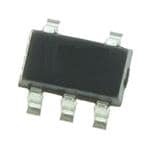
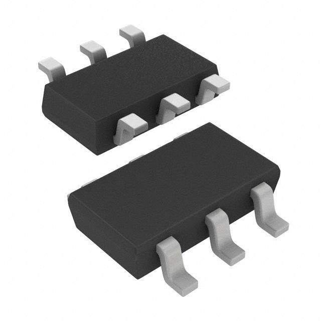
| 描述 | IC REG LDO 1.8V 0.15A SOT23-5低压差稳压器 150mA LDO w/Shtdn |
| 产品分类 | |
| 品牌 | Microchip Technology |
| 产品手册 | |
| 产品图片 |
|
| rohs | 符合RoHS无铅 / 符合限制有害物质指令(RoHS)规范要求 |
| 产品系列 | 电源管理 IC,低压差稳压器,Microchip Technology TC1185-1.8VCT713- |
| 数据手册 | http://www.microchip.com/mymicrochip/filehandler.aspx?ddocname=en026002http://www.microchip.com/mymicrochip/filehandler.aspx?ddocname=en011417http://www.microchip.com/mymicrochip/filehandler.aspx?ddocname=en023833 |
| 产品型号 | TC1185-1.8VCT713 |
| PSRR/纹波抑制—典型值 | 64 dB |
| 产品目录页面 | |
| 产品种类 | 低压差稳压器 |
| 供应商器件封装 | SOT-23-5 |
| 其它名称 | TC11851.8VCT713CT |
| 包装 | 剪切带 (CT) |
| 商标 | Microchip Technology |
| 回动电压—最大值 | 400 mV |
| 安装类型 | 表面贴装 |
| 安装风格 | SMD/SMT |
| 封装 | Reel |
| 封装/外壳 | SC-74A,SOT-753 |
| 封装/箱体 | SOT-23A-5 |
| 工作温度 | -40°C ~ 125°C |
| 工厂包装数量 | 3000 |
| 最大工作温度 | + 125 C |
| 最大输入电压 | 6 V |
| 最小工作温度 | - 40 C |
| 最小输入电压 | 2.7 V |
| 标准包装 | 1 |
| 电压-跌落(典型值) | 0.27V @ 150mA |
| 电压-输入 | 2.7 V ~ 6 V |
| 电压-输出 | 1.8V |
| 电压调节准确度 | 2.5 % |
| 电流-输出 | 150mA |
| 电流-限制(最小值) | - |
| 稳压器拓扑 | 正,固定式 |
| 稳压器数 | 1 |
| 线路调整率 | 0.05 % |
| 负载调节 | 0.5 % |
| 输出电压 | 1.8 V |
| 输出电流 | 150 mA |
| 输出端数量 | 1 Output |
| 输出类型 | Fixed |


- 商务部:美国ITC正式对集成电路等产品启动337调查
- 曝三星4nm工艺存在良率问题 高通将骁龙8 Gen1或转产台积电
- 太阳诱电将投资9.5亿元在常州建新厂生产MLCC 预计2023年完工
- 英特尔发布欧洲新工厂建设计划 深化IDM 2.0 战略
- 台积电先进制程称霸业界 有大客户加持明年业绩稳了
- 达到5530亿美元!SIA预计今年全球半导体销售额将创下新高
- 英特尔拟将自动驾驶子公司Mobileye上市 估值或超500亿美元
- 三星加码芯片和SET,合并消费电子和移动部门,撤换高东真等 CEO
- 三星电子宣布重大人事变动 还合并消费电子和移动部门
- 海关总署:前11个月进口集成电路产品价值2.52万亿元 增长14.8%


PDF Datasheet 数据手册内容提取
TC1014/TC1015/TC1185 50mA, 100mA and 150mA CMOS LDOs with Shutdown and Reference Bypass Features Device Selection Table • ExtremelyLowSupplyCurrent(50µA,Typ.) Junction PartNumber Package (cid:127) VeryLowDropoutVoltage Temp.Range (cid:127) Choiceof50mA(TC1014),100mA(TC1015)and TC1014-xxVCT 5-PinSOT-23A -40°Cto+125°C 150mA(TC1016)Output TC1015-xxVCT 5-PinSOT-23A -40°Cto+125°C (cid:127) HighOutputVoltageAccuracy TC1185-xxVCT 5-PinSOT-23A -40°Cto+125°C (cid:127) StandardorCustomOutputVoltages (cid:127) PowerSavingShutdownMode NOTE: xx indicates output voltages. Available output (cid:127) ReferenceBypassInputforUltraLow-Noise voltages:1.8,2.5,2.6,2.7,2.8,2.85,3.0,3.3,3.6,4.0,5.0. Operation Otheroutputvoltagesareavailable.PleasecontactMicrochip (cid:127) OverCurrentandOverTemperatureProtection TechnologyInc.fordetails. (cid:127) Space-Saving5-PinSOT-23APackage Package Type (cid:127) PinCompatibleUpgradesforBipolarRegulators 5-Pin SOT-23A Applications VOUT Bypass (cid:127) BatteryOperatedSystems (cid:127) PortableComputers 5 4 (cid:127) MedicalInstruments TC1014 (cid:127) Instrumentation TC1015 (cid:127) Cellular/GSM/PHSPhones TC1185 (cid:127) LinearPost-RegulatorforSMPS • Pagers 1 2 3 VIN GND SHDN NOTE:5-PinSOT-23AisequivalenttotheEIAJ(SC-74A) 2002MicrochipTechnologyInc. DS21335B-page 1
TC1014/TC1015/TC1185 GeneralDescription TypicalApplication The TC1014/TC1015/TC1185 are high accuracy 1 5 (typically ±0.5%) CMOS upgrades for older (bipolar) VIN VIN VOUT VOUT lowdropoutregulatorssuchastheLP2980.Designed TC1014 + specificallyfor battery-operated systems, the devices’ TC1015 1µF CMOSconstructioneliminateswastedgroundcurrent, TC1185 2 significantlyextendingbatterylife.Totalsupplycurrent GND istypically50µAatfullload(20to60timeslowerthan inbipolarregulators). Thedevices’keyfeaturesincludeultralownoiseoper- 3 4 ation(plusoptionalBypassinput),fastresponsetostep SHDN Bypass changes in load, and very low dropout voltage – 470pF typically 85mV (TC1014); 180mV (TC1015); and Reference 270mV(TC1185)atfullload.Supplycurrentisreduced Bypass Cap to 0.5µA (max) and V falls to zero when the (Optional) OUT shutdown input is low. The devices incorporate both over-temperatureandover-currentprotection. Shutdown Control TheTC1014/TC1015/TC1185arestablewithanoutput (from Power Control Logic) capacitor of only 1µF and have a maximum output currentof50mA,100mAand150mA,respectively.For higher output current regulators, please see the TC1107/TC1108/TC1173(I =300mA)datasheets. OUT DS21335B-page 2 2002MicrochipTechnologyInc.
TC1014/TC1015/TC1185 1.0 ELECTRICAL Stresses above those listed under "Absolute Maximum Ratings"maycausepermanentdamagetothedevice.These CHARACTERISTICS arestressratingsonlyandfunctionaloperationofthedevice Absolute Maximum Ratings* attheseoranyotherconditionsabovethoseindicatedinthe operation sections of the specifications is not implied. InputVoltage.........................................................6.5V Exposure to Absolute Maximum Rating conditions for extendedperiodsmayaffectdevicereliability. OutputVoltage...........................(-0.3V)to(V +0.3V) IN PowerDissipation...............InternallyLimited(Note7) MaximumVoltageonAnyPin.........V +0.3Vto-0.3V IN OperatingTemperatureRange......-40°C<T <125°C J StorageTemperature.........................-65°Cto+150°C TC1014/TC1015/TC1185ELECTRICALSPECIFICATIONS ElectricalCharacteristics:V =V +1V,I =100µA,C =3.3µF,SHDN>V ,T =25°C,unlessotherwisenoted.Boldfacetype IN R L L IH A specificationsapplyforjunctiontemperaturesof-40°Cto+125°C. Symbol Parameter Min Typ Max Units Device TestConditions V InputOperatingVoltage 2.7 — 6.0 V Note1 IN I MaximumOutputCurrent 50 — — mA TC1014 OUTMAX 100 — — TC1015 150 — — TC1185 V OutputVoltage V –2.5% V ±0.5% V +2.5% V Note2 OUT R R R TCV V TemperatureCoefficient — 20 — ppm/°C Note3 OUT OUT — 40 — ∆V /∆V LineRegulation — 0.05 0.35 % (V +1V)≤ V ≤ 6V OUT IN R IN ∆V /V LoadRegulation — 0.5 2 % TC1014;TC1015 I =0.1mAtoI OUT OUT L OUTMAX — 0.5 3 TC1185 I =0.1mAtoI L OUTMAX (Note4) V -V DropoutVoltage — 2 — mV I =100µA IN OUT L — 65 — I =20mA L — 85 120 I =50mA L — 180 250 TC1015;TC1185 I =100mA L — 270 400 TC1185 I =150mA(Note5) L I SupplyCurrent(Note8) — 50 80 µA SHDN=V ,I =0 IN IH L I ShutdownSupplyCurrent — 0.05 0.5 µA SHDN=0V INSD PSRR PowerSupplyRejection — 64 — dB F ≤ 1kHz RE Ratio I OutputShortCircuitCurrent — 300 450 mA V =0V OUTSC OUT ∆V /∆P ThermalRegulation — 0.04 — V/W Notes6,7 OUT D T ThermalShutdownDie — 160 — °C SD Temperature ∆T ThermalShutdown — 10 — °C SD Hysteresis eN OutputNoise — 600 — nV/√Hz I =I ,F=10kHz L OUTMAX 470pFfromBypass toGND Note 1: TheminimumVINhastomeettwoconditions:VIN≥2.7VandVIN≥VR+VDROPOUT. 2: V istheregulatoroutputvoltagesetting.Forexample:V =1.8V,2.5V,2.6V,2.7V,2.8V,2.85V,3.0V,3.3V,3.6V,4.0V,5.0V. R R 3: TCVOUT=(VOUTMAX–VOUTMIN)x106 VOUTx∆T 4: Regulationismeasuredataconstantjunctiontemperatureusinglowdutycyclepulsetesting.Loadregulationistestedoveraloadrange from1.0mAtothemaximumspecifiedoutputcurrent.Changesinoutputvoltageduetoheatingeffectsarecoveredbythethermal regulationspecification. 5: Dropoutvoltageisdefinedastheinputtooutputdifferentialatwhichtheoutputvoltagedrops2%belowitsnominalvalueata1V differential. 6: ThermalRegulationisdefinedasthechangeinoutputvoltageatatimeTafterachangeinpowerdissipationisapplied,excludingloador lineregulationeffects.SpecificationsareforacurrentpulseequaltoILMAXatVIN=6VforT=10msec. 7: Themaximumallowablepowerdissipationisafunctionofambienttemperature,themaximumallowablejunctiontemperatureandthe thermalresistancefromjunction-to-air(i.e.,TA,TJ,θJA).Exceedingthemaximumallowablepowerdissipationcausesthedevicetoinitiate thermalshutdown.PleaseseeSection4.0ThermalConsiderationsformoredetails. 8: ApplyforJunctionTemperaturesof-40°Cto+85°C. 2002MicrochipTechnologyInc. DS21335B-page 3
TC1014/TC1015/TC1185 TC1014/TC1015/TC1185ELECTRICALSPECIFICATIONS (CONTINUED) ElectricalCharacteristics:V =V +1V,I =100µA,C =3.3µF,SHDN>V ,T =25°C,unlessotherwisenoted.Boldfacetype IN R L L IH A specificationsapplyforjunctiontemperaturesof-40°Cto+125°C. Symbol Parameter Min Typ Max Units TestConditions SHDNInput V SHDNInputHighThreshold 45 — — %V V =2.5Vto6.5V IH IN IN V SHDNInputLowThreshold — — 15 %V V =2.5Vto6.5V IL IN IN Note 1: TheminimumVINhastomeettwoconditions:VIN≥2.7VandVIN≥VR+VDROPOUT. 2: V istheregulatoroutputvoltagesetting.Forexample:V =1.8V,2.5V,2.6V,2.7V,2.8V,2.85V,3.0V,3.3V,3.6V,4.0V,5.0V. R R 3: TCV =(V –V )x106 OUT OUTMAX OUTMIN VOUTx∆T 4: Regulationismeasuredataconstantjunctiontemperatureusinglowdutycyclepulsetesting.Loadregulationistestedoveraloadrange from1.0mAtothemaximumspecifiedoutputcurrent.Changesinoutputvoltageduetoheatingeffectsarecoveredbythethermal regulationspecification. 5: Dropoutvoltageisdefinedastheinputtooutputdifferentialatwhichtheoutputvoltagedrops2%belowitsnominalvalueata1V differential. 6: ThermalRegulationisdefinedasthechangeinoutputvoltageatatimeTafterachangeinpowerdissipationisapplied,excludingloador lineregulationeffects.SpecificationsareforacurrentpulseequaltoILMAXatVIN=6VforT=10msec. 7: Themaximumallowablepowerdissipationisafunctionofambienttemperature,themaximumallowablejunctiontemperatureandthe thermalresistancefromjunction-to-air(i.e.,TA,TJ,θJA).Exceedingthemaximumallowablepowerdissipationcausesthedevicetoinitiate thermalshutdown.PleaseseeSection4.0ThermalConsiderationsformoredetails. 8: ApplyforJunctionTemperaturesof-40°Cto+85°C. DS21335B-page 4 2002MicrochipTechnologyInc.
TC1014/TC1015/TC1185 2.0 PIN DESCRIPTIONS ThedescriptionsofthepinsarelistedinTable2-1. TABLE2-1: PINFUNCTIONTABLE PinNo. Symbol Description (5-PinSOT-23A) 1 V Unregulatedsupplyinput. IN 2 GND Groundterminal. 3 SHDN Shutdowncontrolinput.Theregulatorisfullyenabledwhena logichighisappliedtothisinput. Theregulatorentersshutdownwhenalogiclowisappliedtothisinput.Duringshutdown, outputvoltagefallstozero,ERRORisopencircuitedandsupplycurrentisreducedto0.5µA (max). 4 Bypass Referencebypassinput.Connectinga470pFtothisinputfurtherreducesoutputnoise. 5 V Regulatedvoltageoutput. OUT 2002MicrochipTechnologyInc. DS21335B-page 5
TC1014/TC1015/TC1185 3.0 DETAILED DESCRIPTION 3.1 Bypass Input The TC1014/TC1015/TC1185 are precision fixed A470pFcapacitorconnectedfromtheBypassinputto output voltage regulators. (If an adjustable version is ground reduces noise present on the internal desired,pleaseseetheTC1070/TC1071/TC1187data reference, which in turn significantly reduces output sheet.)Unlikebipolarregulators,theTC1014/TC1015/ noise.Ifoutputnoiseisnotaconcern,thisinputmaybe TC1185 supply current does not increase with load left unconnected. Larger capacitor values may be current. In addition, V remains stable and within used,butresultsinalongertimeperiodtoratedoutput OUT regulation over the entire 0mA to I operating voltagewhenpowerisinitiallyapplied. OUTMAX loadcurrentranges(animportantconsiderationinRTC 3.2 Output Capacitor andCMOSRAMbatteryback-upapplications). Figure3-1 shows a typical application circuit. The A1µF(min)capacitorfromV togroundisrequired. OUT regulator is enabled any time the shutdown input The output capacitor should have an effective series (SHDN) is at or above VIH, and shutdown (disabled) resistancegreaterthan0.1Ω andlessthan5Ω.A1µF when SHDN is at or below VIL. SHDN may be capacitorshouldbeconnectedfromVINtoGNDifthere controlled by a CMOS logic gate, or I/O port of a is more than 10 inches of wire between the regulator microcontroller. If the SHDN input is not required, it andtheACfiltercapacitor,orifabatteryisusedasthe shouldbeconnecteddirectlytotheinputsupply.While power source. Aluminum electrolytic or tantalum in shutdown, supply current decreases to 0.05µA capacitor types can be used. (Since many aluminum (typical),VOUTfallstozerovolts. electrolytic capacitors freeze at approximately -30°C, solid tantalums are recommended for applications FIGURE3-1: TYPICALAPPLICATION operatingbelow-25°C.) Whenoperatingfromsources CIRCUIT other than batteries, supply-noise rejection and transientresponsecanbeimprovedby increasingthe valueoftheinputandoutputcapacitorsandemploying + VIN VOUT VOUT passivefilteringtechniques. 1µF TC1014 + + 1µF TC1015 TC1185 Battery GND SHDN Bypass 470pF Reference Bypass Cap (Optional) Shutdown Control (to CMOS Logic or Tie to VIN if unused) DS21335B-page 6 2002MicrochipTechnologyInc.
TC1014/TC1015/TC1185 4.0 THERMAL CONSIDERATIONS Equation4-1canbeusedinconjunctionwithEquation 4-2 to ensure regulator thermal operation is within 4.1 ThermalShutdown limits.Forexample: Given: Integrated thermal protection circuitry shuts the regulator off when die temperature exceeds 160°C. VINMAX =3.0V+10% The regulator remains off until the die temperature V =2.7V–2.5% OUTMIN dropstoapproximately150°C. I =40mA LOADMAX 4.2 PowerDissipation TJMAX =125°C T =55°C The amount of power the regulator dissipates is AMAX Find: 1.Actualpowerdissipation primarily a function of input and output voltage, and 2.Maximumallowabledissipation output current. The following equation is used to calculateworstcaseactualpowerdissipation: Actualpowerdissipation: P ≈(V –V )I EQUATION4-1: D INMAX OUTMIN LOADMAX =[(3.0x1.1)–(2.7x.975)]40x10–3 P ≈(V –V )I D INMAX OUTMIN LOADMAX =26.7mW Where: Maximumallowablepowerdissipation: P =Worstcaseactualpowerdissipation D P =(T –T ) V =MaximumvoltageonV DMAX JMAX AMAX INMAX IN θ V =Minimumregulatoroutputvoltage JA OUTMIN I =Maximumoutput(load)current =(125–55) LOADMAX 220 The maximum allowable power dissipation (Equation =318mW 4-2)isafunctionofthemaximumambienttemperature Inthisexample,theTC1014dissipatesamaximumof (T ), the maximum allowable die temperature AMAX 26.7mW; below the allowable limit of 318mW. In a (T )andthe thermal resistancefromjunction-to-air JMAX similarmanner,Equation4-1andEquation4-2canbe (θ ). The 5-Pin SOT-23A package has a θ of JA JA used to calculate maximum current and/or input approximately220°C/Watt. voltagelimits. EQUATION4-2: 4.3 Layout Considerations PDMAX=(TJMAX–TAMAX) Theprimarypathofheatconductionoutofthepackage θ JA is via the package leads. Therefore, layouts having a Wherealltermsarepreviouslydefined. groundplane,widetracesatthepads,andwidepower supply bus lines combine to lower θ and therefore JA increase the maximum allowable power dissipation limit. 2002MicrochipTechnologyInc. DS21335B-page 7
TC1014/TC1015/TC1185 5.0 TYPICAL CHARACTERISTICS (UnlessOtherwiseSpecified,AllPartsAreMeasuredAtTemperature=25°C) Note: Thegraphsandtablesprovidedfollowingthisnoteareastatisticalsummarybasedonalimitednumberof samplesandareprovidedforinformationalpurposesonly.Theperformancecharacteristicslistedhereinare nottestedorguaranteed.Insomegraphsortables,thedatapresentedmaybeoutsidethespecified operatingrange(e.g.,outsidespecifiedpowersupplyrange)andthereforeoutsidethewarrantedrange. Dropout Voltage vs. Temperature Dropout Voltage vs. Temperature 0.020 0.100 0.018 VOUT = 3.3V 0.090 VOUT = 3.3V GE (V) 00..001146 ILOAD = 10mA GE (V) 00..007800 ILOAD = 50mA A A DROPOUT VOLT 0000000.......000000000000110246802 CCIONU =T 1=µ 1FµF DROPOUT VOLT 000000......000000123456000000 CCIONU =T 1=µ 1FµF -40 -20 0 20 50 70 125 0.000 TEMPERATURE (°C) -40 -20 0 20 50 70 125 TEMPERATURE (°C) Dropout Voltage vs. Temperature Dropout Voltage vs. Temperature 0.200 0.300 OPOUT VOLTAGE (V)0000000.......001111168024680000000 IVLOOUATD == 31.030VmA OPOUT VOLTAGE (V) 0000....112205050000 VILOOUATD == 31.530VmA DR000...000024000 CCIONU =T 1=µ 1FµF DR 00..000500 CCIONU =T 1=µ 1FµF -40 -20 0 20 50 70 125 -40 -20 0 20 50 70 125 T E MPERA T U R E (°C) TEMPERATURE (°C) Ground Current vs. VIN Ground Current vs. VIN 90 90 80 V OUT = 3.3V 80 VOUT = 3.3V ILOAD = 10mA ILOAD = 100mA µA) 70 A) 70 RENT ( 5600 µENT ( 5600 CUR 40 URR 40 GND 123000 CCIONU =T 1=µ 1FµF GND C 123000 CIN = 1µF 0 COUT = 1µF 00 00..55 1111..55 22 22..55 33 33..55 44 44..55 55 55..55 66 66..55 77 77..55 0 V I N ( V) 0 0.5 11 11..55 22 22..55 33 33..55 44 44..55 55 55..55 66 66..55 77 77..55 VIN (V) DS21335B-page 8 2002MicrochipTechnologyInc.
TC1014/TC1015/TC1185 5.0 TYPICAL CHARACTERISTICS (CONTINUED) (UnlessOtherwiseSpecified,AllPartsAreMeasuredAtTemperature=25°C) Ground Current vs. VIN VOUT vs. VIN 80 3.5 VOUT = 3.3V VOUT = 3.3V 70 ILOAD = 150mA 3 ILOAD = 0 A) 60 2.5 µ NT ( 50 V) 2 RE 40 ( T CUR 30 VOU1.5 D N 1 G 20 10 CCIONU =T 1=µ 1FµF 0.5 CCIONU =T 1=µ 1FµF 0 0 0 0.5 1 11..55 22 22..55 33 33..55 44 44..55 55 55..55 66 66..55 77 77..55 00 00..55 11 11.5.5 22 22..55 33 33..55 44 44..55 55 5 5..55 66 66..55 77 VIN (V) VIN (V) VOUT vs. VIN Output Voltage vs. Temperature 3.5 3.320 3.0 IVILLOOOUAATDD === 311.00300VmmAA 3.315 VILOOUATD == 31.03mVA 2.5 3.310 3.305 V) 2.0 ( UT (V)T3.300 VO1.5 OU3.295 V 1.0 3.290 00..05 CCIONU =T 1=µ 1FµF 33..228805 CCVIIONNU ==T 41=.µ 31FVµF 0 0.5 1 1.5 2 2.5 3 3.5 4 4.5 5 5.5 6 6.5 7 3.275 VIN (V) -40 -20 -10 0 20 40 85 125 TEMPERATURE (°C) Output Voltage vs. Temperature 3.290 VOUT = 3.3V 3.288 ILOAD = 150mA 3.286 3.284 V) (T3.282 U O V 3.280 3.278 CIN = 1µF 3.276 COUT = 1µF VIN = 4.3V 3.274 -40 -20 -10 0 20 40 85 125 TEMPERATURE (°C) 2002MicrochipTechnologyInc. DS21335B-page 9
TC1014/TC1015/TC1185 5.0 TYPICAL CHARACTERISTICS (CONTINUED) (UnlessOtherwiseSpecified,AllPartsAreMeasuredAtTemperature=25°C) Output Voltage vs. Temperature Output Voltage vs. Temperature 5.025 4.994 5.020 VILOOUATD == 51V0mA 44..999902 VILOOUATD == 51V50mA 5.015 4.988 V (V)OUT 555...000001050 V (V)OUT 444...999888246 444...999899505 CVCIIONNU ==T 61=Vµ 1FµF 444...999778680 VCCIIONNU ==T 61=Vµ 1FµF 4.974 -40 -20 -10 0 20 40 85 125 -40 -20 -10 0 20 40 85 125 TEMPERATURE (°C) TEMPERATURE (°C) Temperature vs. Quiescent Current Temperature vs. Quiescent Current 70 80 VOUT = 5V 70 VOUT = 5V A) 60 ILOAD = 10mA µA) 60 ILOAD = 150mA µT ( 50 NT ( 50 EN 40 RE 40 R R R U 30 GND CU 2300 CIN = 1µF GND C 1200 CVCIIONNU ==T 61=Vµ 1FµF 10 COUT = 1µF 0 VIN = 6V -40 -20 -10 0 20 40 85 125 0 TEMPERATURE (°C) -40 -20 -10 0 20 40 85 125 TEMPERATURE (°C) Output Noise vs. Frequency Stability Region vs. Load Current Power Supply Rejection Ratio 10.0 RCLOOUATD = =1 µ5F0Ω 1000 CtoO 1U0Tµ =F 1µF --3350 IVOINUDT C= =1 04mVA µ√NOISE (V/Hz) 1.0 CCIBNY =P 1=µ 0F ΩCESR()OUT 101001 SSttaabbllee RReeggiioonn PSRR (dB) ------445566050550 VVCCIOIONNUUA =TTC 0= == 3 11Vµ0F0mVp-p 0.1 0.1 -70 -75 0.0 0.01 -80 0.01K 0.1K 1K 10K 100K 1000K 0 10 20 30 40 50 60 70 80 90100 0.01K 0.1K 1K 10K 100K 1000K FREQUENCY (Hz) LOAD CURRENT (mA) FREQUENCY (Hz) DS21335B-page 10 2002MicrochipTechnologyInc.
TC1014/TC1015/TC1185 5.0 TYPICAL CHARACTERISTICS (CONTINUED) Measure Rise Time of 3.3V LDO With Bypass Capacitor Measure Rise Time of 3.3V LDO Without Bypass Capacitor Conditions: CIN = 1µF, COUT = 1µF, CBYP = 470pF, ILOAD = 100mA Conditions: CIN = 1µF, COUT = 1µF, CBYP = 0pF, ILOAD = 100mA VIN = 4.3V, Temp = 25°C, Rise Time = 448µS VIN = 4.3V, Temp = 25°C, Rise Time = 184µS VSHDN VSHDN VOUT VOUT Measure Fall Time of 3.3V LDO With Bypass Capacitor Measure Fall Time of 3.3V LDO Without Bypass Capacitor ConditionsV: ICNI N= =4 .13µVF, ,T CemOUpT = = 2 15µ°CF,, CFaBlYl PT i=m 4e7 0=p 1F0,0 IµLSOAD = 50mA ConditionsV: ICNI N= =4 .13µVF, ,T CemOUpT = = 2 15µ°CF,, CFaBlYl PT i=m 0ep =F ,5 I2LµOSAD = 100mA VSHDN VSHDN VOUT VOUT 2002MicrochipTechnologyInc. DS21335B-page11
TC1014/TC1015/TC1185 5.0 TYPICAL CHARACTERISTICS (CONTINUED) Measure Rise Time of 5.0V LDO With Bypass Capacitor Measure Rise Time of 5.0V LDO Without Bypass Capacitor Conditions: VCININ = = 6 1Vµ,F T, eCmOpU T= =2 51°µCF,, RCiBseY PT =im 4e7 0=p 3F9,0 IµLOSAD = 100mA ConditionsV: ICNI N= =6V 1,µ TFe, mCpO U=T 2 =5 °1Cµ,F R, iCsBe YTPim = e0 p=F 1,9 I2LOµSAD = 100mA VSHDN VSHDN VOUT VOUT Measure Fall Time of 5.0V LDO With Bypass Capacitor Measure Fall Time of 5.0V LDO Without Bypass Capacitor Conditions:V CININ = = 6 1Vµ, FT,e CmOpU T= =2 51°µCF, ,F CaBllY TPi m= e4 7=0 1p6F7, µILSOAD = 50mA Conditions:V CININ = = 6 1Vµ, FT,e CmOpU T= =2 51°µCF, ,F CaBllY TPi m= e0 p=F 8, 8ILµOSAD = 100mA VSHDN VSHDN VOUT VOUT DS21335B-page 12 2002MicrochipTechnologyInc.
TC1014/TC1015/TC1185 5.0 TYPICAL CHARACTERISTICS (CONTINUED) Load Regulation of 3.3V LDO Load Regulation of 3.3V LDO Conditions: CIN = 1µF, COUT = 2.2µF, CBYP = 470pF, Conditions: CIN = 1µF, COUT = 2.2µF, CBYP = 470pF, VIN = VOUT + 0.25V, Temp = 25°C VIN = VOUT + 0.25V, Temp = 25°C ILOAD = 50mA switched in at 10kHz, VOUT is AC coupled ILOAD = 100mA switched in at 10kHz, VOUT is AC coupled ILOAD ILOAD VOUT VOUT Load Regulation of 3.3V LDO Line Regulation of 3.3V LDO Conditions: CIN = 1µF, COUT = 2.2µF, CBYP = 470pF, Conditions: VIN = 4V, + 1V Squarewave @2.5kHz VIN = VOUT + 0.25V, Temp = 25°C ILOAD = 150mA switched in at 10kHz, VOUT is AC coupled ILOAD VIN VOUT VOUT CIN = 0µF, COUT = 1µF, CBYP = 470pF, ILOAD = 100mA, VIN & VOUT are AC coupled 2002MicrochipTechnologyInc. DS21335B-page13
TC1014/TC1015/TC1185 5.0 TYPICAL CHARACTERISTICS (CONTINUED) Line Regulation of 5.0V LDO Thermal Shutdown Response of 5.0V LDO Conditions: VIN = 6V, + 1V Squarewave @2.5kHz Conditions: VIN = 6V, CIN = 0µF, COUT = 1µF VIN VOUT VOUT CIN = 0µF, COUT = 1µF, CBYP = 470pF, ILOAD = 100mA, VIN & VOUT are AC coupled ILOAD was increased until temperature of die reached about 160°C, at which time integrated thermal protection circuitry shuts the regulator off when die temperature exceeds approximately 160°C. The regulator remains off until die temperature drops to approximately 150°C. DS21335B-page 14 2002MicrochipTechnologyInc.
TC1014/TC1015/TC1185 6.0 PACKAGING INFORMATION 6.1 Package Marking Information “1”&“2”=partnumbercode+temperaturerangeand voltage TC1014 TC1015 TC1185 (V) Code Code Code 1.8 AY BY NY 2.5 A1 B1 N1 2.6 NB BT NT 2.7 A2 B2 N2 2.8 AZ BZ NZ 2.85 A8 B8 N8 3.0 A3 B3 N3 3.3 A5 B5 N5 3.6 A9 B9 N9 4.0 A0 B0 N0 5.0 A7 B7 N7 “3”representsdatecode “4”representslotIDnumber 6.2 Taping Form Component Taping Orientation for 5-Pin SOT-23A (EIAJ SC-74A) Devices User Direction of Feed Device Marking W PIN 1 P Standard Reel Component Orientation TR Suffix Device (Mark Right Side Up) Carrier Tape, Number of Components Per Reel and Reel Size Package Carrier Width (W) Pitch (P) Part Per Full Reel Reel Size 5-Pin SOT-23A 8 mm 4 mm 3000 7 in 2002MicrochipTechnologyInc. DS21335B-page15
TC1014/TC1015/TC1185 6.3 Package Dimensions SOT-23A-5 .075 (1.90) REF. .122 (3.10) .071 (1.80) .098 (2.50) .059 (1.50) .020 (0.50) .012 (0.30) .037 (0.95) PIN 1 REF. .122 (3.10) .106 (2.70) .057 (1.45) .035 (0.90) 10° MAX. .010 (0.25) .004 (0.09) .006 (0.15) .024 (0.60) .000 (0.00) .004 (0.10) Dimensions: inches (mm) DS21335B-page 16 2002MicrochipTechnologyInc.
TC1014/TC1015/TC1185 SalesandSupport DataSheets ProductssupportedbyapreliminaryDataSheetmayhaveanerratasheetdescribingminoroperationaldifferencesandrecom- mendedworkarounds.Todetermineifanerratasheetexistsforaparticulardevice,pleasecontactoneofthefollowing: 1. YourlocalMicrochipsalesoffice 2. TheMicrochipCorporateLiteratureCenterU.S.FAX:(480)792-7277 3. TheMicrochipWorldwideSite(www.microchip.com) Pleasespecifywhichdevice,revisionofsiliconandDataSheet(includeLiterature#)youareusing. NewCustomerNotificationSystem Registeronourwebsite(www.microchip.com/cn)toreceivethemostcurrentinformationonourproducts. 2002 Microchip Technology Inc. DS21335B-page17
TC1014/TC1015/TC1185 NOTES: DS21335B-page18 2002 Microchip Technology Inc.
TC1014/TC1015/TC1185 Information contained in this publication regarding device Trademarks applicationsandthelikeisintendedthroughsuggestiononly andmaybesupersededbyupdates.Itisyourresponsibilityto The Microchip name and logo, the Microchip logo, FilterLab, ensure that your application meets with your specifications. KEELOQ, microID, MPLAB, PIC, PICmicro, PICMASTER, No representation or warranty is given and no liability is PICSTART,PROMATE, SEEVAL and TheEmbedded Control assumedbyMicrochipTechnologyIncorporatedwithrespect SolutionsCompanyareregisteredtrademarksofMicrochipTech- totheaccuracyoruseofsuchinformation,orinfringementof nologyIncorporatedintheU.S.A.andothercountries. patentsorotherintellectualpropertyrightsarisingfromsuch dsPIC,ECONOMONITOR,FanSense,FlexROM,fuzzyLAB, useorotherwise.UseofMicrochip’sproductsascriticalcom- In-Circuit Serial Programming, ICSP, ICEPIC, microPort, ponentsinlifesupportsystemsisnotauthorizedexceptwith Migratable Memory, MPASM, MPLIB, MPLINK, MPSIM, expresswritten approvalbyMicrochip.Nolicensesarecon- MXDEV,MXLAB,PICC,PICDEM,PICDEM.net,rfPIC,Select veyed,implicitlyorotherwise,underanyintellectualproperty Mode and Total Endurance are trademarks of Microchip rights. TechnologyIncorporatedintheU.S.A. SerializedQuickTurnProgramming(SQTP)isaservicemark ofMicrochipTechnologyIncorporatedintheU.S.A. All other trademarks mentioned herein are property of their respectivecompanies. © 2002, Microchip Technology Incorporated, Printed in the U.S.A.,AllRightsReserved. Printedonrecycledpaper. MicrochipreceivedQS-9000qualitysystem certificationforitsworldwideheadquarters, designandwaferfabricationfacilitiesin ChandlerandTempe,ArizonainJuly1999 andMountainView,CaliforniainMarch2002. TheCompany’squalitysystemprocessesand proceduresareQS-9000compliantforits PICmicro®8-bitMCUs,KEELOQ®codehopping devices,SerialEEPROMs,microperipherals, non-volatilememoryandanalogproducts.In addition,Microchip’squalitysystemforthe designandmanufactureofdevelopment systemsisISO9001certified. 2002MicrochipTechnologyInc. DS21335B-page19
WORLDWIDE SALES AND SERVICE AMERICAS ASIA/PACIFIC Japan CorporateOffice Australia MicrochipTechnologyJapanK.K. BenexS-16F 2355WestChandlerBlvd. MicrochipTechnologyAustraliaPtyLtd 3-18-20,Shinyokohama Chandler,AZ 85224-6199 Suite22,41RawsonStreet Kohoku-Ku,Yokohama-shi Tel: 480-792-7200 Fax: 480-792-7277 Epping2121,NSW Kanagawa,222-0033,Japan TechnicalSupport:480-792-7627 Australia Tel:81-45-471-6166 Fax:81-45-471-6122 WebAddress:http://www.microchip.com Tel:61-2-9868-6733Fax:61-2-9868-6755 Korea RockyMountain China-Beijing 2355WestChandlerBlvd. Microchip Technology Consulting (Shanghai) MicrochipTechnologyKorea 168-1,YoungboBldg.3Floor Chandler,AZ 85224-6199 Co.,Ltd.,BeijingLiaisonOffice Samsung-Dong,Kangnam-Ku Tel: 480-792-7966 Fax: 480-792-7456 Unit915 BeiHaiWanTaiBldg. Seoul,Korea135-882 Atlanta Tel:82-2-554-7200 Fax:82-2-558-5934 No.6ChaoyangmenBeidajie 500SugarMillRoad,Suite200B Beijing,100027,No.China Singapore Atlanta,GA 30350 Tel:86-10-85282100Fax:86-10-85282104 MicrochipTechnologySingaporePteLtd. Tel:770-640-0034 Fax:770-640-0307 China-Chengdu 200MiddleRoad Boston #07-02PrimeCentre Microchip Technology Consulting (Shanghai) 2LanDrive,Suite120 Singapore,188980 Co.,Ltd.,ChengduLiaisonOffice Westford,MA 01886 Tel: 65-6334-8870 Fax:65-6334-8850 Rm.2401,24thFloor, Tel:978-692-3848 Fax:978-692-3821 MingXingFinancialTower Taiwan Chicago No.88TIDUStreet MicrochipTechnologyTaiwan 333PierceRoad,Suite180 Chengdu610016,China 11F-3,No.207 Itasca,IL 60143 Tel:86-28-86766200 Fax:86-28-86766599 TungHuaNorthRoad Tel:630-285-0071Fax:630-285-0075 Taipei,105,Taiwan China-Fuzhou Dallas Tel:886-2-2717-7175 Fax:886-2-2545-0139 Microchip Technology Consulting (Shanghai) 4570WestgroveDrive,Suite160 Co.,Ltd.,FuzhouLiaisonOffice Addison,TX75001 Unit28F,WorldTradePlaza EUROPE Tel:972-818-7423 Fax:972-818-2924 No.71WusiRoad Detroit Fuzhou350001,China Denmark Tri-AtriaOfficeBuilding Tel:86-591-7503506 Fax:86-591-7503521 MicrochipTechnologyNordicApS 32255NorthwesternHighway,Suite190 China-Shanghai RegusBusinessCentre FarmingtonHills,MI 48334 Microchip Technology Consulting (Shanghai) Lautruphoj1-3 Tel:248-538-2250Fax:248-538-2260 BallerupDK-2750Denmark Co.,Ltd. Kokomo Room701,Bldg.B Tel:4544209895Fax:4544209910 2767S.AlbrightRoad FarEastInternationalPlaza France Kokomo,Indiana 46902 No.317XianXiaRoad MicrochipTechnologySARL Tel:765-864-8360Fax:765-864-8387 Shanghai,200051 Parcd’ActiviteduMoulindeMassy LosAngeles Tel:86-21-6275-5700 Fax:86-21-6275-5060 43RueduSauleTrapu 18201VonKarman,Suite1090 China-Shenzhen BatimentA-lerEtage Irvine,CA 92612 Microchip Technology Consulting (Shanghai) 91300Massy,France Tel:949-263-1888 Fax:949-263-1338 Co.,Ltd.,ShenzhenLiaisonOffice Tel:33-1-69-53-63-20 Fax:33-1-69-30-90-79 NewYork Rm.1315,13/F,ShenzhenKerryCentre, Germany 150MotorParkway,Suite202 RenminnanLu MicrochipTechnologyGmbH Hauppauge,NY 11788 Shenzhen518001,China Gustav-HeinemannRing125 Tel:631-273-5305 Fax:631-273-5335 Tel:86-755-2350361 Fax:86-755-2366086 D-81739Munich,Germany SanJose China-HongKongSAR Tel:49-89-627-1440 Fax:49-89-627-144-44 Italy MicrochipTechnologyInc. MicrochipTechnologyHongkongLtd. 2107NorthFirstStreet,Suite590 Unit901-6,Tower2,Metroplaza MicrochipTechnologySRL SanJose,CA 95131 223HingFongRoad CentroDirezionaleColleoni Tel:408-436-7950 Fax:408-436-7955 KwaiFong,N.T.,HongKong PalazzoTaurus1V.LeColleoni1 Toronto Tel:852-2401-1200 Fax:852-2401-3431 20041AgrateBrianza Milan,Italy 6285NorthamDrive,Suite108 India Tel:39-039-65791-1 Fax:39-039-6899883 Mississauga,OntarioL4V1X5,Canada MicrochipTechnologyInc. UnitedKingdom Tel:905-673-0699 Fax: 905-673-6509 IndiaLiaisonOffice DivyasreeChambers MicrochipLtd. 505EskdaleRoad 1Floor,WingA(A3/A4) WinnershTriangle No.11,O’ShaugnesseyRoad Bangalore,560025,India Wokingham Berkshire,EnglandRG415TU Tel:91-80-2290061Fax:91-80-2290062 Tel:441189215869 Fax:44-118921-5820 05/01/02 *DS21335B* DS21335B-page 20 2002MicrochipTechnologyInc.
Mouser Electronics Authorized Distributor Click to View Pricing, Inventory, Delivery & Lifecycle Information: M icrochip: TC1015-1.8VCT713 TC1014-2.8VCT713 TC1185-2.8VCT713 TC1185-2.5VCT713 TC1185-2.7VCT713 TC1185- 2.6VCT713 TC1185-3.3VCT713 TC1185-3.0VCT713 TC1185-3.6VCT713 TC1185-4.0VCT713 TC1014-1.8VCT713 TC1015-2.85VCT713 TC1185-2.85VCT713 TC1014-2.85VCT713 TC1015-2.8VCT713 TC1015-2.5VCT713 TC1015- 2.7VCT713 TC1015-2.6VCT713 TC1014-3.0VCT713 TC1014-3.3VCT713 TC1014-3.6VCT713 TC1015-3.3VCT713 TC1015-3.0VCT713 TC1015-3.6VCT713 TC1015-5.0VCT713 TC1014-5.0VCT713 TC1014-2.5VCT713 TC1014- 2.6VCT713 TC1014-4.0VCT713 TC1015-4.0VCT713 TC1185-5.0VCT713 TC1185-1.8VCT713