ICGOO在线商城 > TAS5624ADDV
 Datasheet下载
- 型号: TAS5624ADDV
- 制造商: Texas Instruments
- 库位|库存: xxxx|xxxx
- 要求:
| 数量阶梯 | 香港交货 | 国内含税 |
| +xxxx | $xxxx | ¥xxxx |
查看当月历史价格
查看今年历史价格
TAS5624ADDV产品简介:
ICGOO电子元器件商城为您提供TAS5624ADDV由Texas Instruments设计生产,在icgoo商城现货销售,并且可以通过原厂、代理商等渠道进行代购。 提供TAS5624ADDV价格参考以及Texas InstrumentsTAS5624ADDV封装/规格参数等产品信息。 你可以下载TAS5624ADDV参考资料、Datasheet数据手册功能说明书, 资料中有TAS5624ADDV详细功能的应用电路图电压和使用方法及教程。
| 参数 | 数值 |
| 产品目录 | 集成电路 (IC)半导体 |
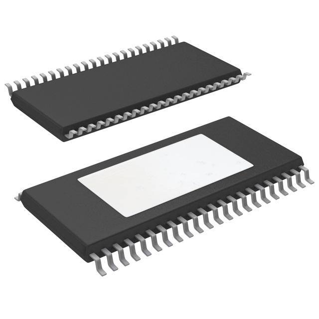
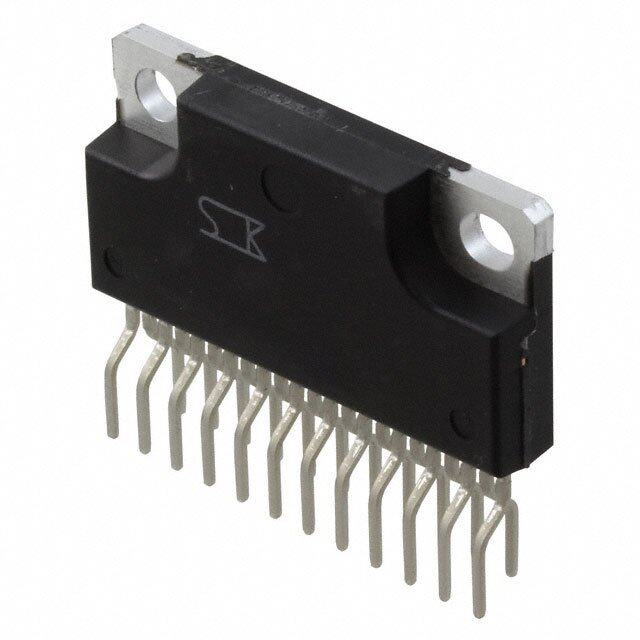
| 描述 | IC AMP AUD 150W STER D 44HTSSOP音频放大器 150W St/300W Mono HD Dig-In Pwr Stage |
| 产品分类 | |
| 品牌 | Texas Instruments |
| 产品手册 | http://www.ti.com/lit/gpn/tas5624a |
| 产品图片 |
|
| rohs | 符合RoHS无铅 / 符合限制有害物质指令(RoHS)规范要求 |
| 产品系列 | 音频 IC,音频放大器,Texas Instruments TAS5624ADDVPurePath™ HD |
| 数据手册 | |
| 产品型号 | TAS5624ADDV |
| Pd-功率耗散 | 1 W |
| THD+噪声 | 0.025 % |
| 不同负载时的最大输出功率x通道数 | 400W x 1 @ 1.5 欧姆; 200W x 2 @ 3 欧姆 |
| 产品 | Audio Amplifiers |
| 产品种类 | 音频放大器 |
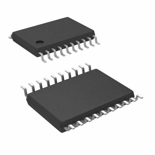
| 供应商器件封装 | 44-HTSSOP |
| 其它名称 | 296-30496-5 |
| 包装 | 管件 |
| 商标 | Texas Instruments |
| 安装类型 | 表面贴装 |
| 安装风格 | SMD/SMT |
| 封装 | Tube |
| 封装/外壳 | 44-TSSOP (0.244",6.20mm 宽)裸焊盘 |
| 封装/箱体 | HTSSOP-44 |
| 工作温度 | 0°C ~ 70°C (TA) |
| 工厂包装数量 | 35 |
| 最大功率耗散 | 1 W |
| 标准包装 | 35 |
| 特性 | 消除爆音,数字输入,短路和热保护,关机 |
| 电压-电源 | 12 V ~ 38 V |
| 电源电流 | 20 mA |
| 类 | Class-D |
| 类型 | D 类 |
| 系列 | TAS5624A |
| 输出功率 | 150 W |
| 输出类型 | 1-通道(单声道)或 2-通道(立体声) |


- 商务部:美国ITC正式对集成电路等产品启动337调查
- 曝三星4nm工艺存在良率问题 高通将骁龙8 Gen1或转产台积电
- 太阳诱电将投资9.5亿元在常州建新厂生产MLCC 预计2023年完工
- 英特尔发布欧洲新工厂建设计划 深化IDM 2.0 战略
- 台积电先进制程称霸业界 有大客户加持明年业绩稳了
- 达到5530亿美元!SIA预计今年全球半导体销售额将创下新高
- 英特尔拟将自动驾驶子公司Mobileye上市 估值或超500亿美元
- 三星加码芯片和SET,合并消费电子和移动部门,撤换高东真等 CEO
- 三星电子宣布重大人事变动 还合并消费电子和移动部门
- 海关总署:前11个月进口集成电路产品价值2.52万亿元 增长14.8%


PDF Datasheet 数据手册内容提取
Product Sample & Technical Tools & Support & Folder Buy Documents Software Community TAS5624A SLAS844A–MAY2012–REVISEDJANUARY2016 TAS5624A 150-W Stereo and 300-W Mono PurePath™ HD Digital Input Class-D Power Stage 1 Features 3 Description • PurePath™HDIntegratedFeedbackProvides: The TAS5624A device is a thermally-enhanced 1 version of the class-D power amplifier based on the – 0.025%THDat1Winto4 Ω TAS5614A using large MOSFETs for improved power – > 65-dBPSRR(NoInputSignal) efficiency and a novel gate-drive scheme for reduced – > 105-dB(A-Weighted)SNR losses in idle and at low-output signals leading to reducedheatsinksize. • PreclippingOutputforControlofaClass-GPower Supply The unique preclipping output signal can be used to control a Class-G power supply. This combined with • ReducedHeatSinkSizeDuetoUseof40-mΩ the low idle loss and high power efficiency of the OutputMOSFETWith > 90%EfficiencyatFull TAS5624A leads to industry leading levels of OutputPower efficiencyensuringasuper greensystem. • OutputPowerat10%THD+N The TAS5624A uses constant voltage gain. The – 150-Wand4-Ω BTLStereoConfiguration internally-matched gain resistors ensure a high power – 300-Wand2-Ω PBTLMonoConfiguration supply rejection ratio giving an output voltage only • OutputPowerat10%THD+N dependent on the audio input voltage and free from anypowersupplyartifacts. – 125-Wand4-Ω BTLStereoConfiguration – 250-Wand2-Ω PBTLMonoConfiguration The high integration of the TAS5624A makes the amplifier easy to use; and, using TI’s reference • Click-FreeandPop-FreeStart-Up schematics and PCB layouts leads to fast design in • ErrorReportingSelf-ProtectedDesignWithUVP, time. The TAS5624A is available in the space-saving, Overtemperature,andShort-CircuitProtection surface-mount44-pinHTSSOPpackage. • EMI-CompliantWhenUsedWithRecommended DeviceInformation(1) SystemDesign PARTNUMBER PACKAGE BODYSIZE(NOM) • 44-PinHTSSOP(DDV)PackageforReduced BoardSize TAS5624A HTSSOP(44) 14.00mm×6.10mm (1) For all available packages, see the orderable addendum at 2 Applications theendofthedatasheet. • Blu-ray™andDVDReceivers TypicalTAS5624AApplicationBlockDiagram • High-PowerSoundBars • PoweredSubwooferandActiveSpeakers • MiniComboSystems TASxxxx PurePathHDTM DigitalAudio TASTA56S305624A DIGITAL Processor AUDIO INPUT +12V 18V-36V PurePathHDTM +3.3V REG. Class G Power Supply Ref design 105VAC→240VAC 1 An IMPORTANT NOTICE at the end of this data sheet addresses availability, warranty, changes, use in safety-critical applications, intellectualpropertymattersandotherimportantdisclaimers.PRODUCTIONDATA.
TAS5624A SLAS844A–MAY2012–REVISEDJANUARY2016 www.ti.com Table of Contents 1 Features.................................................................. 1 9.2 FunctionalBlockDiagrams.....................................12 2 Applications........................................................... 1 9.3 FeatureDescription.................................................14 3 Description............................................................. 1 9.4 DeviceFunctionalModes........................................18 4 RevisionHistory..................................................... 2 10 ApplicationandImplementation........................ 19 10.1 ApplicationInformation..........................................19 5 DeviceComparisonTable..................................... 3 10.2 TypicalApplications..............................................19 6 PinConfigurationandFunctions......................... 4 11 PowerSupplyRecommendations..................... 27 7 Specifications......................................................... 6 11.1 PowerSupplies.....................................................27 7.1 AbsoluteMaximumRatings......................................6 11.2 BootStrapSupply.................................................27 7.2 ESDRatings ............................................................6 12 Layout................................................................... 28 7.3 RecommendedOperatingConditions.......................6 12.1 LayoutGuidelines.................................................28 7.4 ThermalInformation..................................................7 12.2 LayoutExample....................................................30 7.5 ElectricalCharacteristics...........................................7 13 DeviceandDocumentationSupport................. 32 7.6 ElectricalCharacteristics–AudioSpecification Stereo(BTL)..............................................................8 13.1 DeviceSupport ....................................................32 7.7 ElectricalCharacteristics–AudioSpecification4 13.2 DocumentationSupport .......................................32 Channels(SE)............................................................8 13.3 CommunityResources..........................................32 7.8 ElectricalCharacteristics–AudioSpecificationMono 13.4 Trademarks...........................................................32 (PBTL)....................................................................... 9 13.5 ElectrostaticDischargeCaution............................32 7.9 TypicalCharacteristics..............................................9 13.6 Glossary................................................................32 8 ParameterMeasurementInformation................12 14 Mechanical,Packaging,andOrderable 9 DetailedDescription............................................ 12 Information........................................................... 32 9.1 Overview.................................................................12 4 Revision History NOTE:Pagenumbersforpreviousrevisionsmaydifferfrompagenumbersinthecurrentversion. ChangesfromOriginal(May2012)toRevisionA Page • AddedESDRatingstable,FeatureDescriptionsection,DeviceFunctionalModes,ApplicationandImplementation section,PowerSupplyRecommendationssection,Layoutsection,DeviceandDocumentationSupportsection,and Mechanical,Packaging,andOrderableInformationsection. ................................................................................................ 1 2 SubmitDocumentationFeedback Copyright©2012–2016,TexasInstrumentsIncorporated ProductFolderLinks:TAS5624A
TAS5624A www.ti.com SLAS844A–MAY2012–REVISEDJANUARY2016 5 Device Comparison Table FEATURES TAS5624A TAS5612A TAS5612LA TAS5614A TAS5614LA TAS5622A MaximumPowertoSingle- 75 65 75 65 EndedLoad MaximumPowertoBridge 200 165 125 200 150 150 TiedLoad MaximumPowertoParallel 400 250 250 300 300 300 BridgeTiedLoad MinimumSupportedSingle- 2 2 2 2 EndedLoad MinimumSupportedBridge 3 3 4 3 4 3 TiedLoad MinimumSupportedParallel 1.5 2 2 2 2 2 BridgeTiedLoad Closed-LoopandOpen-Loop Closed Closed Closed Closed Closed Closed MaximumSpeakerOutputs(#) 4 2 4 2 4 2 InputType PWM PWM PWM PWM PWM PWM ControlType Hardware Hardware Hardware Hardware Hardware Hardware Copyright©2012–2016,TexasInstrumentsIncorporated SubmitDocumentationFeedback 3 ProductFolderLinks:TAS5624A
TAS5624A SLAS844A–MAY2012–REVISEDJANUARY2016 www.ti.com 6 Pin Configuration and Functions DDVPackage 44-PinHTSSOP TopView GGVVDDDD__AABB BST_A VDD BST_B OC_ADJ GND RESET GND INPUT_A OUT_A INPUT_B OUT_A C_START PVDD_AB DVDD PVDD_AB GND PVDD_AB GND OUT_B GND GND GND GND AVDD OUT_C INPUT_C PVDD_CD INPUT_D PVDD_CD FAULT PVDD_CD OTW OUT_D CLIP OUT_D M1 GND M2 GND M3 BST_C GVDD_CD BST_D PinFunctions PIN TYPE(1) DESCRIPTION(2) NAME NO. AVDD 13 P Internalvoltageregulator,analogsection BST_A 44 P Bootstrappin,A-side BST_B 43 P Bootstrappin,B-side BST_C 24 P Bootstrappin,C-side BST_D 23 P Bootstrappin,D-side C_START 7 O Start-upramp CLIP 18 O Clippingwarning;open-drain;active-low DVDD 8 P Internalvoltageregulator,digitalsection FAULT 16 O Shutdownsignal,open-drain;active-low 9,10,11,12,25, GND P Ground 26,33,34,41,42 GVDD_AB 1 P Gate-drivevoltagesupply;AB-side GVDD_CD 22 P Gate-drivevoltagesupply;CD-side INPUT_A 5 I PWMInputsignalforhalf-bridgeA INPUT_B 6 I PWMInputsignalforhalf-bridgeB INPUT_C 14 I PWMInputsignalforhalf-bridgeC INPUT_D 15 I PWMInputsignalforhalf-bridgeD M1 19 I Modeselection1(LSB) M2 20 I Modeselection2 M3 21 I Modeselection3(MSB) (1) I=Input,O=Output,andP=Power (2) Locatedonthetopsideofthedeviceforconvenientthermalcouplingtotheheatsink. 4 SubmitDocumentationFeedback Copyright©2012–2016,TexasInstrumentsIncorporated ProductFolderLinks:TAS5624A
TAS5624A www.ti.com SLAS844A–MAY2012–REVISEDJANUARY2016 PinFunctions(continued) PIN TYPE(1) DESCRIPTION(2) NAME NO. OC_ADJ 3 O Overcurrentthresholdprogrammingpin OTW 17 O Overtemperaturewarning;open-drain;active-low OUT_A 39,40 O Output,half-bridgeA OUT_B 35 O Output,half-bridgeB OUT_C 32 O Output,half-bridgeC OUT_D 27,28 O Output,half-bridgeD PowerPAD™ — P Ground,connecttogroundedheatsink PVDD_AB 36,37,38 P PVDDsupplyforhalf-bridgeAandB PVDD_CD 29,30,31 P PVDDsupplyforhalf-bridgeCandD RESET 4 I DeviceresetInput;active-low VDD 2 P Inputpowersupply ModeSelectionPins MODEPINS PWMInput(1) OUTPUTCONFIGURATION INPUTA INPUTB INPUTC INPUTD MODE M3 M2 M1 0 0 0 2N+1 2×BTL PWMa PWMb PWMc PWMd ADMode 0 0 1 1N+1(2) 2×BTL PWMa Unused PWMc Unused ADMode 0 1 0 2N+1 2×BTL PWMa PWMb PWMc PWMd BDMode 0 1 1 1N+1(2) 1×BTL+2×SE PWMa Unused PWMc PWMd ADMode 1 0 0 2N+1 1×PBTL PWMa PWMb 0 0 ADMode 1 0 0 1N+1(2) 1×PBTL PWMa Unused 0 1 ADMode 1 0 0 2N+1 1×PBTL PWMa PWMb 1 0 BDMode 1 0 1 1N+1 4×SE(3) PWMa PWMb PWMc PWMd ADMode (1) The1Nand2NnamingconventionisusedtoindicatethenumberofPWMlinestothepowerstageperchannelinaspecificmode. (2) Using1NinterfaceinBTLandPBTLmoderesultsinincreasedDCoffsetontheoutputterminals. (3) The4×SEmodecanbeusedas1×BTL+2×SEconfigurationbyfeedinga2NPWMsignaltoeitherINPUT_ABorINPUT_CDfor improvedDCoffsetaccuracy Copyright©2012–2016,TexasInstrumentsIncorporated SubmitDocumentationFeedback 5 ProductFolderLinks:TAS5624A
TAS5624A SLAS844A–MAY2012–REVISEDJANUARY2016 www.ti.com 7 Specifications 7.1 Absolute Maximum Ratings overoperatingfree-airtemperaturerangeunlessotherwisenoted(1) MIN MAX UNIT VDDtoGND,GVDD_X(2)toGND –0.3 13.2 V PVDD_X(2)toGND,OUT_XtoGND,BST_XtoGVDD_X(2) –0.3 50 V BST_XtoGND(3) –0.3 62.5 V DVDDtoGND –0.3 4.2 V AVDDtoGND –0.3 8.5 V OC_ADJ,M1,M2,M3,C_START,INPUT_XtoGND –0.3 4.2 V RESET,FAULT,OTW,CLIP,toGND –0.3 4.2 V Maximumcontinuoussinkcurrent(FAULT,OTW,CLIP) 9 mA Maximumoperatingjunctiontemperature,T 0 150 °C J Leadtemperature 260 260 °C Storagetemperature,T –40 150 °C stg (1) StressesbeyondthoselistedunderAbsoluteMaximumRatingsmaycausepermanentdamagetothedevice.Thesearestressratings only,andfunctionaloperationofthedeviceattheseoranyotherconditionsbeyondthoseindicatedunderRecommendedOperating Conditionsisnotimplied.Exposuretoabsolute-maximum-ratedconditionsforextendedperiodsmayaffectdevicereliability. (2) GVDD_XandPVDD_Xrepresentsafull-bridgegatedriveorpowersupply.GVDD_XisGVDD_ABorGVDD_CD,PVDD_Xis PVDD_ABorPVDD_CD (3) MaximumBST_XtoGNDvoltageisthesumofmaximumPVDDtoGNDandGVDDtoGNDvoltagesminusadiodedrop. 7.2 ESD Ratings VALUE UNIT Electrostatic Human-bodymodel(HBM),perANSI/ESDA/JEDECJS-001(1) ±2000 V V (ESD) discharge Charged-devicemodel(CDM),perJEDECspecificationJESD22-C101(2) ±500 (1) JEDECdocumentJEP155statesthat500-VHBMallowssafemanufacturingwithastandardESDcontrolprocess. (2) JEDECdocumentJEP157statesthat250-VCDMallowssafemanufacturingwithastandardESDcontrolprocess. 7.3 Recommended Operating Conditions MIN NOM MAX UNIT PVDD_X Full-bridgesupply DCsupplyvoltage 12 36 38 V Supplyforlogicregulatorsandgate-drive GVDD_X DCsupplyvoltage 10.8 12 13.2 V circuitry VDD Digitalregulatorsupplyvoltage DCsupplyvoltage 10.8 12 13.2 V BTL 2.5 4 Outputfilter:L=10uH,1µF. R Loadimpedance SE OutputADmodulation, 1.5 3 Ω L switchingfrequency>350kHz. PBTL 1.5 2 Minimuminductanceatovercurrentlimit, L Outputfilterinductance includinginductortolerance,temperature 5 μH OUTPUT andpossibleinductorsaturation F PWMframerate 352 384 500 kHz PWM C PVDDclosedecouplingcapacitors 0.44 1 μF PVDD BTLandPBTLconfiguration 100 nF C_START Start-uprampcapacitor SEand1×BTL+2×SEconfiguration 1 μF R Overcurrentprogrammingresistor Resistortolerance=5% 24 33 kΩ OC R Overcurrentprogrammingresistor Resistortolerance=5% 47 62 68 kΩ OC_LATCHED T Junctiontemperature 0 125 °C J 6 SubmitDocumentationFeedback Copyright©2012–2016,TexasInstrumentsIncorporated ProductFolderLinks:TAS5624A
TAS5624A www.ti.com SLAS844A–MAY2012–REVISEDJANUARY2016 7.4 Thermal Information TAS5624A THERMALMETRIC(1) DDV(HTSSOP) UNIT 44PINS R Junction-to-ambientthermalresistance 1.9 °C/W θJA R Junction-to-case(top)thermalresistance 0.6 °C/W θJC(top) R Junction-to-boardthermalresistance 1.7 °C/W θJB ψ Junction-to-topcharacterizationparameter 0.6 °C/W JT ψ Junction-to-boardcharacterizationparameter 1.7 °C/W JB R Junction-to-case(bottom)thermalresistance — °C/W θJC(bot) (1) Formoreinformationabouttraditionalandnewthermalmetrics,seetheSemiconductorandICPackageThermalMetricsapplication report,SPRA953. 7.5 Electrical Characteristics PVDD_X=36V,GVDD_X=12V,VDD=12V,T (casetemperature)=75°C,f =384kHz,unlessotherwisespecified. C S PARAMETER TESTCONDITIONS MIN TYP MAX UNIT INTERNALVOLTAGEREGULATORANDCURRENTCONSUMPTION Voltageregulator,onlyusedasareference DVDD VDD=12V 3 3.3 3.6 V node Voltageregulator,onlyusedasareference AVDD VDD=12V 7.8 V node Operating,50%dutycycle 20 IVDD VDDsupplycurrent mA Idle,resetmode 20 50%dutycycle 12 IGVDD_X Gate-supplycurrentperfull-bridge mA Resetmode 3 50%dutycyclewithoutload 15 IPVDD_X Full-bridgeidlecurrent RESETlow 1.9 mA VDDandGVDD_Xat0V 0.4 OUTPUT-STAGEMOSFETs RDS(on),LS Drain-to-sourceresistance,low-side(LS) TJ=25°C,excludesmetallizationresistance, 40 mΩ RDS(on),HS Drain-to-sourceresistance,high-side(HS) GVDD=12V 40 mΩ I/OPROTECTION Vuvp,GVDD Undervoltageprotectionlimit,GVDD_X 8.5 V Vuvp,GVDD,hyst(1) Undervoltageprotectionlimit,GVDD_X 0.7 V Vuvp,VDD Undervoltageprotectionlimit,VDD 8.5 V Vuvp,VDD,hyst(1) Undervoltageprotectionlimit,VDD 0.7 V Vuvp,PVDD Undervoltageprotectionlimit,PVDD_X 8.5 V Vuvp,PVDD,hyst(1) Undervoltageprotectionlimit,PVDD_X 0.7 V OTW(1) Overtemperaturewarning 115 125 135 °C TemperaturedropneededbelowOTW OTWhyst(1) temperatureforOTWtobeinactiveafter 25 °C OTWevent. OTE(1) Overtemperatureerror 145 155 165 °C OTE-OTWdifferential(1) OTE-OTWdifferential 30 °C OTEHYST(1) AaftdeervaicneOrTesEeetvisennteededtoclearFAULT 25 °C OLPC Overloadprotectioncounter fPWM=384kHz 2.6 ms Resistor-programmable,nominalpeakcurrentin IOC Overcurrentlimitprotection 1-Ωload,ROC=24kΩ 15 A Resistor-programmable,nominalpeakcurrentin IOC_LATCHED Overcurrentlimitprotection,latched 1-Ωload,ROC=62kΩ 15 A TimefromapplicationofshortconditiontoHi-Zof IOCT Overcurrentresponsetime affectedhalf-bridge 150 ns Internalpulldownresistoratoutputofeach ConnectedwhenRESETisactivetoprovide IPD half-bridge bootstrapcharge.NotusedinSEmode. 3 mA (1) Specifiedbydesign. Copyright©2012–2016,TexasInstrumentsIncorporated SubmitDocumentationFeedback 7 ProductFolderLinks:TAS5624A
TAS5624A SLAS844A–MAY2012–REVISEDJANUARY2016 www.ti.com Electrical Characteristics (continued) PVDD_X=36V,GVDD_X=12V,VDD=12V,T (casetemperature)=75°C,f =384kHz,unlessotherwisespecified. C S PARAMETER TESTCONDITIONS MIN TYP MAX UNIT STATICDIGITALSPECIFICATIONS VIH Highlevelinputvoltage 1.9 V INPUT_X,M1,M2,M3,RESET VIL Lowlevelinputvoltage 0.8 V LEAKAGE Inputleakagecurrent 100 μA OTW/SHUTDOWN(FAULT) Internalpullupresistance,OTW,CLIP, RINT_PU FAULTtoDVDD 20 26 33 kΩ VOH Highleveloutputvoltage Internalpullupresistor 3 3.3 3.6 V VOL Lowleveloutputvoltage IO=4mA 200 500 mV FANOUT DevicefanoutOTW,FAULT,CLIP Noexternalpullup 30 devices 7.6 Electrical Characteristics – Audio Specification Stereo (BTL) AudioperformanceisrecordedasachipsetconsistingofaTAS55588-ChannelHDCompatibleAudioProcessorwithASRC andPWMOutput(SLES273),PWMProcessor(modulationindexlimitedto97.7%)andaTAS5624ApowerstagewithPCB andsystemconfigurationsinaccordancewithrecommendedguidelines. Audiofrequency=1kHz,PVDD_X=36V,GVDD_X=12V,R =4Ω,f =384kHz,R =24kΩ,T =75°C,OutputFilter: L S OC C L =10μH,C =1µF,unlessotherwisenoted. DEM DEM PARAMETER TESTCONDITIONS MIN TYP MAX UNIT R =3Ω,10%THD+N 200 L R =4Ω,10%THD+N 150 L P Poweroutputperchannel W O R =3Ω,1%THD+N 160 L R =4Ω,1%THD+N 125 L THD+N Totalharmonicdistortion+noise 1-W,1-kHzsignal 0.025% V Outputintegratednoise A-weighted,AES17measuringfilter 180 μV n V Outputoffsetvoltage Nosignal 10 20 mV OS SNR Signal-to-noiseratio(1) A-weighted,AES17measuringfilter 105 dB DNR Dynamicrange A-weighted,–60dBFS(rel1%THD+N) 105 dB P Powerdissipationduetoidlelosses P =0,channelsswitching(2) 1 W idle (IPVDD_X) O (1) SNRiscalculatedrelativeto1%THD-Noutputlevel. (2) Actualsystemidlelossesalsoareaffectedbycorelossesofoutputinductors. 7.7 Electrical Characteristics – Audio Specification 4 Channels (SE) AudioperformanceisrecordedasachipsetconsistingofaTASxxxx,PWMProcessor(modulationindexlimitedto97.7%) andaTAS5624ApowerstagewithPCBandsystemconfigurationsinaccordancewithrecommendedguidelines. Audiofrequency=1kHz,PVDD_X=36V,GVDD_X=12V,R =4Ω,f =384kHz,R=24kΩ,T =75°C,OutputFilter: L S C L =10μH,C =1µF,C =470µF,unlessotherwisenoted. DEM DEM DCB PARAMETER TESTCONDITIONS MIN TYP MAX UNIT R =3Ω,10%THD+N 50 L P Poweroutputperchannel W O R =3Ω,1%THD+N 42 L THD+N Totalharmonicdistortion+noise 1-W,1-kHzsignal 0.025% V Outputintegratednoise A-weighted,AES17measuringfilter 180 μV n SNR Signal-to-noiseratio(1) A-weighted,AES17measuringfilter 102 dB DNR Dynamicrange A-weighted,–60dBFS(rel1%THD+N) 102 dB P PowerdissipationduetoIdlelosses P =0,channelsswitching(2) 1 W idle (IPVDD_X) O (1) SNRiscalculatedrelativeto1%THD-Noutputlevel. (2) Actualsystemidlelossesalsoareaffectedbycorelossesofoutputinductors. 8 SubmitDocumentationFeedback Copyright©2012–2016,TexasInstrumentsIncorporated ProductFolderLinks:TAS5624A
TAS5624A www.ti.com SLAS844A–MAY2012–REVISEDJANUARY2016 7.8 Electrical Characteristics – Audio Specification Mono (PBTL) AudioperformanceisrecordedasachipsetconsistingofaTASxxxx,PWMProcessor(modulationindexlimitedto97.7%) andaTAS5624ApowerstagewithPCBandsystemconfigurationsinaccordancewithrecommendedguidelines. Audiofrequency=1kHz,PVDD_X=36V,GVDD_X=12V,R =4Ω,f =384kHz,R =24kΩ,T =75°C,OutputFilter: L S OC C L =10μH,C =1μF,unlessotherwisenoted. DEM DEM PARAMETER TESTCONDITIONS MIN TYP MAX UNIT R =1.5Ω,10%,THD+N 400 L R =2Ω,10%THD+N 300 L R =4Ω,10%THD+N 160 L P Poweroutputperchannel W O R =1.5Ω,1%THD+N 320 L R =2Ω,1%THD+N 250 L R =4Ω,1%THD+N 130 L THD+N Totalharmonicdistortion+noise 1-W,1-kHzsignal 0.025% V Outputintegratednoise A-weighted,AES17measuringfilter 180 μV n V Outputoffsetvoltage Nosignal 10 20 mV OS SNR Signal-to-noiseratio(1) A-weighted,AES17measuringfilter 105 dB DNR Dynamicrange A-weighted,–60dBFS(rel1%THD) 105 dB P Powerdissipationduetoidlelosses P =0,Allchannelsswitching(2) 1 W idle (IPVDD_X) O (1) SNRiscalculatedrelativeto1%THD-Noutputlevel. (2) Actualsystemidlelossesareaffectedbycorelossesofoutputinductors. 7.9 Typical Characteristics 7.9.1 BTLConfiguration Measurementconditionsare:1kHz,PVDD_X=36V,GVDD_X=12V,R =4Ω,f =384kHz,R =24kΩ,T =75°C, L S OC C OutputFilter:L =10μH,C =1µF,20-Hzto20-kHzBW(AES17lowpassfilter),unlessotherwisenoted. DEM DEM 10 260 3W 3W 4W 240 4W Noise − % 8W 220200 8W N − Total Harmonic Distortion + 0.11 P − Output Power − WO1111168024680000000 HD+ 40 T0.01 TC = 75(cid:176)C 20 TTCH D= +7N5 (cid:176)aCt 10% 0.005 0 0.02 0.1 1 10 100 300 10 15 20 25 30 35 40 PO − Output Power − W G001 PVDD − Supply Voltage − V G003 1kHz Figure1.TotalHarmonic+NoisevsOutputPower Figure2.OutputPowervsSupplyVoltage vsDistortion+Noise=10% Copyright©2012–2016,TexasInstrumentsIncorporated SubmitDocumentationFeedback 9 ProductFolderLinks:TAS5624A
TAS5624A SLAS844A–MAY2012–REVISEDJANUARY2016 www.ti.com BTL Configuration (continued) Measurementconditionsare:1kHz,PVDD_X=36V,GVDD_X=12V,R =4Ω,f =384kHz,R =24kΩ,T =75°C, L S OC C OutputFilter:L =10μH,C =1µF,20-Hzto20-kHzBW(AES17lowpassfilter),unlessotherwisenoted. DEM DEM 10 220 1 W 3W 10 W 200 4W N − Total Harmonic Distortion + Noise − %00.0.111 100 W P − Output Power − WO1111168024680000000 8W D+ 40 H T 20 TC = 75(cid:176)C TC = 75(cid:176)C 0.001 0 20 100 1k 10k 20k 10 15 20 25 30 35 40 Frequency − Hz PVDD − Supply Voltage − V G002 G004 4Ω Figure3.TotalHarmonicDistortion+Noise Figure4.OutputPowervsSupplyVoltage, vsFrequency Distortion+Noise=1% 100 60 95 3Ω 90 55 4Ω 85 50 8Ω 80 75 45 70 65 40 Efficiency−% 4455605050 Power Loss−W 233505 35 20 30 25 15 20 15 3Ω 10 10 4Ω 5 5 8Ω TC= 75°C TC= 75°C 0 0 0 100 200 300 400 500 0 100 200 300 400 500 Total Output Power−W Total Output Power−W G005 G006 Figure5.SystemEfficiencyvsOutputPower Figure6.SystemPowerLossvsOutputPower 260 0 240 −−2100 TVCR E=F 7=5 2(cid:176)C2.5 V 4W 220 −30 Sample Rate = 48kHz FFT Size = 16384 −40 200 −50 P − Output Power − WO 11111802468000000 Noise Amplitude − dB−−−−−−−−−11111987643210000000000 60 −150 −160 40 3W −170 20 4W −180 8W THD+N at 10% −190 0 −200 −10 0 10 20 30 40 50 60 70 80 90 100110 0 2k 4k 6k 8k 10k 12k 14k 16k 18k 20k 22k 24k TC − Case Temperature − (cid:176)C G007 f − Frequency − Hz G008 Figure7.OutputPowervsTemperature Figure8.NoiseAmplitudevsFrequency 10 SubmitDocumentationFeedback Copyright©2012–2016,TexasInstrumentsIncorporated ProductFolderLinks:TAS5624A
TAS5624A www.ti.com SLAS844A–MAY2012–REVISEDJANUARY2016 7.9.2 SEConfiguration Measurementconditionsare:1kHz,PVDD_X=36V,GVDD_X=12V,R =4Ω,f =384kHz,R =24kΩ,T =75°C, L S OC C OutputFilter:L =10μH,C =1µF,C =470µF,20-Hzto20-kHzBW(AES17lowpassfilter),unlessotherwise DEM DEM DCB noted. 10 100 2W 2W 3W 3W Noise − % 4W 80 4W D+N − Total Harmonic Distortion + 0.11 P − Output Power − WO 246000 H T0.01 TC = 75(cid:176)C TTCH D= +7N5 (cid:176)aCt 10% 0.005 0 0.02 0.1 1 10 100 10 15 20 25 30 35 40 PO − Output Power − W G009 PVDD − Supply Voltage − V G010 Figure9.TotalHarmonicDistortion+NoisevsOutput Figure10.OutputPowervsSupplyVoltage Power 7.9.3 PBTLConfiguration Measurementconditionsare:1kHz,PVDD_X=36V,GVDD_X=12V,R =4Ω,f =384kHz,R =24kΩ,T =75°C, L S OC C OutputFilter:L =10μH,C =1µF,20-Hzto20-kHzBW(AES17lowpassfilter),unlessotherwisenoted. DEM DEM 10 450 2W 2W 3W 3W Noise − % 4W 345000 4W N − Total Harmonic Distortion + 0.11 P − Output Power − WO112230505000000 D+ H T0.01 TC = 75(cid:176)C 50 TTCH D= +7N5 (cid:176)aCt 10% 0.005 0 0.02 0.1 1 10 100 500 10 15 20 25 30 35 40 PO − Output Power − W G011 PVDD − Supply Voltage − V G012 Figure11.TotalHarmonicDistortion+Noise Figure12.OutputPowervsSupplyVoltage vsOutputPower Copyright©2012–2016,TexasInstrumentsIncorporated SubmitDocumentationFeedback 11 ProductFolderLinks:TAS5624A
TAS5624A SLAS844A–MAY2012–REVISEDJANUARY2016 www.ti.com 8 Parameter Measurement Information AllparametersaremeasuredaccordingtotheconditionsdescribedintheSpecificationssection. 9 Detailed Description 9.1 Overview TAS5624A is a PWM input, audio PWM (class-D) amplifier. the output of the TAS5624A can be configured for single-ended, bridge-tied load (BTL) or parallel BTL (PBTL) output. It requires two railes for power supply, PVDD and 12 V (GVDD and VDD). Figure 13 shows typical connections for BTL outputs. A detailed schematic can be viewedinTAS5624AEVMUser'sGuide(SLAU376). 9.2 Functional Block Diagrams Capacitors for System External microcontroller Filtering & /AMPRESET Startup/Stop I2C TPAWSMx xMxoxdulVaAtLoIDr *NOTE1 /RESET /FAULT /OTW /CLIP C_START BST_A Bootstrap BST_B Capacitors PWM_A INPUT_A OUT_A 2ndOrder Left- Input Output L-C Output Channel PWM_B INPUT_B H-Bridge1 H-Bridge1 OUT_B Filter for Output each H-Bridge 2-CHANNEL H-BRIDGE BTLMODE PWM_C INPUT_C OUT_C 2ndOrder Right- Input Output L-C Output Channel PWM_D INPUT_D H-Bridge2 H-Bridge2 OUT_D Filter for Output each H-Bridge Hardwire M1 BST_C CMoondtreol MM23 PVDD_AB,CD GND GVDD_AB,CD GND VDD DVDD AVDD OC_ADJ BST_D CBaopoatsctirtoarps PVDD PVDD GVDD,VDD, Hardwire 36V Power Supply &VREG Over- SYSTEM Decoupling Power Supply Current Power Decoupling Limit Supplies GND GND GVDD(12V)/VDD(12V) 12V VAC (1)LogicANDisinsideoroutsidethemicroprocessor Figure13. TypicalSystemBlockDiagram 12 SubmitDocumentationFeedback Copyright©2012–2016,TexasInstrumentsIncorporated ProductFolderLinks:TAS5624A
TAS5624A www.ti.com SLAS844A–MAY2012–REVISEDJANUARY2016 Functional Block Diagrams (continued) /CLIP /OTW /FAULT BST_X UVP GVDD_X AVDD DVDD /RESET MODE1-3 GIC POWER-UP O RESET L AVDD O AVDD &I/ ON TEMP VDD CTI SENSE E T O DVDD PR CB3C OVER- DVDD LOAD PROTECTION STARTUP CONTROL C_START BST_A PVDD_AB INPUT_A REPCWEIMVER ANALOG + PWM& TIMING GATE-DRIVE OUT_A LOOPFILTER - CONTROL GND GVDD_AB BST_B PVDD_AB INPUT_B PWM + PWM& RECEIVER ANALOG TIMING GATE-DRIVE OUT_B LOOPFILTER - CONTROL GND BST_C PVDD_CD INPUT_C PWM + PWM& RECEIVER ANALOG TIMING GATE-DRIVE OUT_C LOOPFILTER - CONTROL GND GVDD_CD BST_D PVDD_CD INPUT_D PWM + PWM& RECEIVER ANALOG TIMING GATE-DRIVE OUT_D LOOPFILTER - CONTROL GND Figure14. FunctionalBlockDiagram Copyright©2012–2016,TexasInstrumentsIncorporated SubmitDocumentationFeedback 13 ProductFolderLinks:TAS5624A
TAS5624A SLAS844A–MAY2012–REVISEDJANUARY2016 www.ti.com 9.3 Feature Description 9.3.1 SystemPower-UpandPower-DownSequence 9.3.1.1 PoweringUp The TAS5624A does not require a power-up sequence. The outputs of the H-bridges remain in a high- impedance state until the gate-drive supply voltage (GVDD_X) and VDD voltage are above the undervoltage protection (UVP) voltage threshold (see the Electrical Characteristics table of this data sheet). Although not specifically required, TI recommends to hold RESET in a low state while powering up the device. This allows an internalcircuittochargetheexternalbootstrapcapacitorsbyenablingaweakpulldownofthehalf-bridgeoutput. 9.3.1.2 PoweringDown The TAS5624A does not require a power-down sequence. The device remains fully operational as long as the gate-drive supply (GVDD_X) voltage and VDD voltage are above the undervoltage protection (UVP) voltage threshold (see the Electrical Characteristics table of this data sheet). Although not specifically required, it is a goodpracticetoholdRESETlowduringpowerdown,thuspreventingaudibleartifactsincludingpopsorclicks. 9.3.2 Start-UpandShutdownRampSequence The integrated start-up and stop sequence ensures a click-free and pop-free start-up and shutdown sequence of the amplifier. The start-up sequence uses a voltage ramp with a duration set by the CSTART capacitor. The sequence uses the input PWM signals to generate output PWM signals, hence input idle PWM must be present duringbothstart-upandshutdownrampingsequences. VDD, GVDD_X and PVDD_X power supplies must be turned on and with settled outputs before starting thestart-uprampbysetting RESEThigh. During start-up and shutdown ramp, the input PWM signals must be in muted condition with the PWM processor noiseshaperactivityturnedoff(50%dutycycle). The duration of the start-up and shutdown ramp is 100 ms + X ms, where X is the CSTART capacitor value in nF. TI recommends using a 100-nF CSTART in BTL and PBTL mode and 1 µF in SE mode configuration. This results in ramp times of 200 ms and 1.1 s respectively. The longer ramp time in SE configuration allows charge anddischargeoftheoutputAC-couplingcapacitorwithoutaudibleartifacts. Ramp Start Ramp End Ramp Start Ramp End 3.3V /RESET 0V 3.3V INPUT_X INPUT_XIS SWITCHING(MUTE) (UNMUTED) INPUT_XIS SWITCHING(MUTE) Hi-Z NOISE SHAPER OFF NOISE SHAPER OFF 0V PVDD_X OUT_X OUT_XIS SWITCHING(MUTE) (UNMUTED) OUT_XIS SWITCHING(MUTE) Hi-Z 0V VI_CM DC_RAMP 0V 50% PVDD_X/2 SPEAKER OUT_X 0V tStartup Ramp tStartup Ramp INPUT_XIS SWITCHING(MUTE) NOISE SHAPER ON Figure15. Start-UpandShutdownRamp 14 SubmitDocumentationFeedback Copyright©2012–2016,TexasInstrumentsIncorporated ProductFolderLinks:TAS5624A
TAS5624A www.ti.com SLAS844A–MAY2012–REVISEDJANUARY2016 Feature Description (continued) 9.3.3 UnusedOutputChannels If all available output channels are not used, TI recommends disabling of unused output nodes to reduce power consumption. Furthermore by disabling unused output channels the cost of unused output LC demodulation filterscanbeavoided. Disablingachannelisdonebyleavethebootstrapcapacitor(BST)unstuffedandconnectingtherespectiveinput toGND.Theunusedoutputpinscanbeleftfloating. NOTE ThePVDDdecouplingcapacitorsmuststillbemounted. Table1.UnusedOutputChannels OPERATIN PWM OUTPUT UNUSED INPUT_A INPUT_B INPUT_C INPUT_D UNSTUFFEDCOMPONENT GMODE INPUT CONFIGURATION CHANNEL 000 2N+1 AB GND GND PWMc PWMd BST_A&BST_Bcapacitor 001 1N+1 2×BTL CD PWMa PWMb GND GND BST_C&BST_Dcapacitor 010 2N+1 A GND PWMb PWMc PWMd BST_Acapacitor B PWMa GND PWMc PWMd BST_Bcapacitor 101 1N+1 4×SE C PWMa PWMb GND PWMd BST_Ccapacitor D PWMa PWMb PWMc GND BST_Dcapacitor 9.3.4 DeviceProtectionSystem TheTAS5624Acontainsadvancedprotectioncircuitrycarefullydesignedtofacilitatesystemintegrationandease of use, as well as to safeguard the device from permanent failure due to a wide range of fault conditions such as short circuits, overload, overtemperature, and undervoltage. The TAS5624A responds to a fault by immediately setting the power stage in a high-impedance (Hi-Z) state and asserting the FAULT pin low. In situations other than overload and overtemperature error (OTE), the device automatically recovers when the fault condition has beenremoved,thatis,thesupplyvoltagehasincreased. Thedevicewillfunctiononerrors,asshowninTable2. Table2.DeviceProtection BTLMODE PBTLMODE SEMODE CHANNELFAULT TURNSOFF CHANNELFAULT TURNSOFF CHANNELFAULT TURNSOFF A A A A+B A+B B B B A+B+C+D C C C C+D C+D D D D BootstrapUVPdoesnotshutdownaccordingtothetable,itshutsdowntherespectivehigh-sideFET. 9.3.5 Pin-to-PinShort-CircuitProtection(PPSC) The PPSC detection system protects the device from permanent damage if a power output pin (OUT_X) is shorted to GND or PVDD_X. For comparison, the OC protection system detects an overcurrent after the demodulationfilterwherePPSCdetectsshortsdirectlyatthepinbeforethefilter.PPSCdetectionisperformedat start-up, for example, when VDD is supplied, consequently a short to either GND or PVDD_X after system start- up does not activate the PPSC detection system. When PPSC detection is activated by a short on the output, all half-bridges are kept in a Hi-Z state until the short is removed, the device then continues the start-up sequence and starts switching. The detection is controlled globally by a two-step sequence. The first step ensures that there are no shorts from OUT_X to GND, the second step tests that there are no shorts from OUT_X to PVDD_X. The total duration of this process is roughly proportional to the capacitance of the output LC filter. The Copyright©2012–2016,TexasInstrumentsIncorporated SubmitDocumentationFeedback 15 ProductFolderLinks:TAS5624A
TAS5624A SLAS844A–MAY2012–REVISEDJANUARY2016 www.ti.com typical duration is < 15 ms/μF. While the PPSC detection is in progress, FAULT is kept low, and the device will not react to changes applied to the RESET pins. If no shorts are present the PPSC detection passes, and FAULT is released. A device reset will not start a new PPSC detection. PPSC detection is enabled in BTL and PBTL output configurations, the detection is not performed in SE mode. To make sure not to trip the PPSC detectionsystem,TIrecommendsnottoinsertresistiveloadtoGNDorPVDD_X. 9.3.6 OvertemperatureProtection The TAS5624A has a two-level, temperature-protection system that asserts an active-low warning signal (OTW) when the device junction temperature exceeds 125°C (typical). If the device junction temperature exceeds 155°C (typical), the device is put into thermal shutdown, resulting in all half-bridge outputs being set in the high- impedance (Hi-Z) state and FAULT being asserted low. OTE is latched in this case. To clear the OTE latch, RESETmustbeasserted.Thereafter,thedeviceresumesnormaloperation. 9.3.7 OvertemperatureWarning, OTW The overtemperature warning OTW asserts when the junction temperature has exceeded recommended operating temperature. Operation at junction temperatures above OTW threshold is exceeding recommended operationconditionsandisstronglyadvisedtoavoid. If OTW asserts, take action to reduce power dissipation to allow junction temperature to decrease until it gets below the OTW hysteresis threshold. This action can be decreasing audio volume or turning on a system cooling fan. 9.3.8 UndervoltageProtection(UVP)andPower-OnReset(POR) The UVP and POR circuits of the TAS5624A fully protect the device in any power-up, power-down, or brownout situation. While powering up, the POR circuit resets the overload circuit (OLP) and ensures that all circuits are fully operational when the GVDD_X and VDD supply voltages reach stated in the Electrical Characteristics table. Although GVDD_X and VDD are independently monitored, a supply voltage drop below the UVP threshold on any VDD or GVDD_X pin results in all half-bridge outputs immediately being set in the high-impedance (Hi-Z) state and FAULT being asserted low. The device automatically resumes operation when all supply voltages have increasedabovetheUVPthreshold. 9.3.9 ErrorReporting NOTE AssertingRESETlowforcestheFAULTsignalhigh,independentoffaultsbeingpresent. TI recommends monitoring the OTW signal using the system microcontroller and responding to an overtemperaturewarningsignalby,forexample,turningdownthevolumetopreventfurtherheatingofthedevice resultingindeviceshutdown(OTE). To reduce external component count, an internal pullup resistor to 3.3 V is provided on FAULT, CLIP, and OTW outputs.SeeElectricalCharacteristicstableforactualvalues. TheFAULTandOTWpinsareactive-low,open-drainoutputs.Theirfunctionisforprotection-modesignalingtoa PWMcontrollerorothersystem-controldevice. Any fault resulting in device shutdown is signaled by the FAULT pin going low. Likewise, OTW goes low when thedevicejunctiontemperatureexceeds125°C(seeTable3). Table3.ErrorReporting FAULT OTW DESCRIPTION 0 0 Overtemperature(OTE)oroverload(OLP)orundervoltage(UVP) 0 1 Overload(OLP)orundervoltage(UVP) 1 0 Junctiontemperaturehigherthan125°C(overtemperaturewarning) 1 1 Junctiontemperaturelowerthan125°CandnoOLPorUVPfaults(normaloperation) 16 SubmitDocumentationFeedback Copyright©2012–2016,TexasInstrumentsIncorporated ProductFolderLinks:TAS5624A
TAS5624A www.ti.com SLAS844A–MAY2012–REVISEDJANUARY2016 9.3.10 FaultHandling Ifafaultsituationoccurswhileinoperation,thedevicewillactaccordinglytothefaultbeingaglobalorachannel fault. A global fault is a chip-wide fault situation and causes all PWM activity of the device to shut down, and will assert FAULT low. A global fault is a latching fault and clearing FAULT and restart operation requires resetting the device by toggling RESET. Toggling RESET must never be allowed with excessive system temperature, so it is advised to monitor RESET by a system microcontroller and only allow releasing RESET (RESET high) if the OTWsignaliscleared(high).AchannelfaultwillresultinshutdownofthePWMactivityoftheaffectedchannels. Asserting RESET low forces the FAULT signal high, independent of faults being present. TI recommends monitoring the OTW signal using the system microcontroller and responding to an overtemperature warning signal by, for example, turning down the volume to prevent further heating of the device resulting in device shutdown(OTE). Table4.FaultHandling FAULTAND GLOBALOR REPORTING LATCHEDAND ACTIONNEEDEDTO FAULTANDEVENT EVENT OUTPUTFETs CHANNEL METHOD SELFCLEARING CLEAR DESCRIPTION PVDD_XUVP VDDUVP Increaseaffectedsupply VoltageFault Global FAULTPin Self-Clearing Hi-Z GVDD_XUVP voltage AVDDUVP PowerOn POR(DVDDUVP) Global FAULTPin Self-Clearing AllowDVDDtorise H-Z Reset Channel AllowBSTcaptorecharge BSTUVP VoltageFault None Self-Clearing HighSideOff (half-bridge) (lowsideon,VDD12V) Thermal CoolbelowlowerOTW OTW Global OTWPin Self-Clearing Normaloperation Warning threshold Thermal OTE(OTSD) Global FAULTPin Latched ToggleRESET Hi-Z Shutdown OLP(CBC>2.6ms) OCshutdown Channel FAULTPin Latched ToggleRESET Hi-Z LatchedOC(ROC>47k) OCshutdown Channel FAULTPin Latched ToggleRESET Hi-Z Reducesignallevelor Flipstate,cycleby CBC(24k<ROC<33k) OCLimiting Channel None Self-Clearing removeshort cycleatfs/2 StuckatFault(1) NoPWM Channel None Self-Clearing ResumePWM Hi-Z (1to3channels) StuckatFault(1) NoPWM Global None Self-Clearing ResumePWM Hi-Z (Allchannels) (1) StuckatFaultoccurswheninputPWMdropsbelowminimumPWMframerategiveninRecommendedOperatingConditions. 9.3.11 DeviceReset When RESET is asserted low, all power-stage FETs in the four half-bridges are forced into a high-impedance (Hi-Z)state. In BTL modes, to accommodate bootstrap charging prior to switching start, asserting the reset input low enables weak pulldown of the half-bridge outputs. In the SE mode, the output is forced into a high impedance state when asserting the reset input low. Asserting reset input low removes any fault information to be signaled on the FAULT output, that is, FAULT is forced high. A rising-edge transition on reset input allows the device to resume operation after an overload fault. To ensure thermal reliability, the rising edge of RESET must occur no sooner than4msafterthefallingedgeofFAULT. 9.3.12 SystemDesignConsideration Arising-edgetransitionon RESETinputallowsthedevicetoexecutethestart-upsequenceandstartsswitching. Apply audio only according to the timing information for start-up and shutdown sequence. That will start and stop theamplifierwithoutaudibleartifactsintheoutputtransducers. The CLIP signal indicates that the output is approaching clipping (when output PWM starts skipping pulses due to loop filter saturation). The signal can be used to initiate an audio volume decrease or to adjust the power supplyrail. Thedeviceinvertstheaudiosignalfrominputtooutput. Copyright©2012–2016,TexasInstrumentsIncorporated SubmitDocumentationFeedback 17 ProductFolderLinks:TAS5624A
TAS5624A SLAS844A–MAY2012–REVISEDJANUARY2016 www.ti.com TheDVDDandAVDDpinsarenotrecommendedtobeusedasavoltagesourceforexternalcircuitry. 9.4 Device Functional Modes There are three main output modes that the user can configure the device as per application requirement. In addition, there are two PWM modulation modes, AD and BD. AD modulation can have single-ended (SE) or differential analog inputs. AD modulation can also be configured to have SE, BTL, BTL + SE, or PBTL outputs. BDmodulationrequiresdifferentialanaloginputs.BDmodulationcanonlybeconfiguredinBTLorPBTLmode. 18 SubmitDocumentationFeedback Copyright©2012–2016,TexasInstrumentsIncorporated ProductFolderLinks:TAS5624A
TAS5624A www.ti.com SLAS844A–MAY2012–REVISEDJANUARY2016 10 Application and Implementation NOTE Information in the following applications sections is not part of the TI component specification, and TI does not warrant its accuracy or completeness. TI’s customers are responsible for determining suitability of components for their purposes. Customers should validateandtesttheirdesignimplementationtoconfirmsystemfunctionality. 10.1 Application Information These typical connection diagrams highlight the required external components and system level connections for proper operation of the device in several popular use cases. Each of these configurations can be realized using the evaluation modules (EVMs) for the device. These flexible modules allow full evaluation of the device in the most common modes of operation. Any design variation can be supported by TI through schematic and layout reviews. Visit the E2E Forum at www.e2e.ti.com for design assistance and join the audio amplifier discussion forumforadditionalinformation. 10.2 Typical Applications 10.2.1 TypicalBTLApplication See Figure 16for application schematic. In this application, differential PWM inputs are used with AD modulation from the PWM modulator (TAS5558). AD modulation scheme is defined as PWM(+) as opposite polarity from PWM(–). Copyright©2012–2016,TexasInstrumentsIncorporated SubmitDocumentationFeedback 19 ProductFolderLinks:TAS5624A
TAS5624A SLAS844A–MAY2012–REVISEDJANUARY2016 www.ti.com 3.3R +12V GND 10uF 100nF 33nF 1 GVDD_AB BST_A 44 100nF 2 VDD BST_B 43 33nF ROC-ADJUST 3 OCA_DJ GND 42 10µH 10nF /RESET 4 /RESET GND 41 1nF 100nF 3R3 PWM_A 5 INPUT_A OUT_A 40 PWM_B 6 INPUT_B OUT_A 39 220nF 220nF 470nF 7 C_START PVDD_AB 38 470uF 3R3 100nF 8 DVDD PVDD_AB 37 100nF 1nF 1uF 9 GND PVDD_AB 36 10nF 10GND OUT_B 35 10µH 11GND TAS5624A GND 34 PVDD GND 1uF 12GND GND 33 13AVDD OUT_C 32 10µH 10nF PWM_C 14INPUT_C PVDD_CD 31 1nF PWM_D 15INPUT_D PVDD_CD 30 100nF 3R3 /FAULT 16/FAULT PVDD_CD 29 470uF 220nF 220nF /OTW 17/OTW OUT_D 28 470nF /CLIP 18/CLIP OUT_D 27 100nF 3R3 19M1 GND 26 1nF 10nF 20M2 GND 25 33nF 21M3 BST_C 24 10µH 100nF 33nF 22GVDD_CD BST_D 23 3.3R Figure16. TypicalDifferential(2N)BTLApplicationWithADModulationFilters 20 SubmitDocumentationFeedback Copyright©2012–2016,TexasInstrumentsIncorporated ProductFolderLinks:TAS5624A
TAS5624A www.ti.com SLAS844A–MAY2012–REVISEDJANUARY2016 10.2.1.1 DesignRequirements Table5liststhedesignparametersofFigure16. Table5.DesignRequirements PARAMETER VALUE Digitalregulatorsupply 12V Full-bridgepowersupply 12Vto38V PWMmodulator TAS5558 Outputfilters Inductor-capacitorlowpassfilter Speaker 2.5Ωminimum 10.2.1.2 DetailedDesignProcedure UsingFigure16asaguide,integratethehardwareintothesystemschematic. Following the recommended component placement, schematic layout and routing given in Layout Example, integratethedeviceanditssupportingcomponentsintothesystemPCBfile. • The most critical section of the circuit is the power supply inputs, the amplifier output signals, and the high- frequency signals which go to the serial audio port. TI recommends that these be constructed to ensure they aregivenprecedentasdesigntrade-offsaremade. • For questions and support go to the E2E Forum at www.e2e.ti.com. If it is necessary to deviate from the recommendedlayout,pleasevisittheE2EForumtorequestalayoutreview. 10.2.1.2.1 PinConnections • Pin 1 - GVDD_AB is the gate-drive voltage for half-bridges A and B. It needs a 3.3-Ω isolation resistor and a 0.1-µFdecouplingcapacitor. • Pin 2 - VDD is the supply for internal voltage regulators AVDD and DVDD. It needs a 10-µF bulk capacitor anda0.1-µFdecouplingcapacitor. • Pin 3 - Roc adjust is the overcurrent programming resistor. Depending on the application, this resistor can be between24kΩ to68kΩ. • Pin4-RESETpinwhenasserted,itkeepsoutputsHi-ZandnoPWMswitching.Thispincanbecontrolledby amicroprocessor. • Pins 5 and 6 - These are PWM(+) and PWM(–) pins with signals provided by a PWM modulator such as the TAS5558.ThesearePWMdifferentialpairs. • Pin7-Start-uprampcapacitormustbe1 µFforSEconfiguration. • Pin8-Digitaloutputsupplypinisconnectedto1-µFdecouplingcapacitor. • Pins9-12-Groundpinsareconnectedtoboardground. • Pin13-Analogoutputsupplypinisconnectedto1-µFdecouplingcapacitor. • Pins 14 and 15 - These are PWM(+) and PWM(–) pins with signals provided by a PWM modulator such as theTAS5558.ThesearePWMdifferentialpair. • Pin 16 - Fault pin can be monitored by a microcontroller through GPIO pin. System can decide to assert reset orshutdown. • Pin 17 - Overtemperature warning pin can be monitored by a microcontroller through a GPIO pin. System can decidetoturnonfanorloweroutputpower. • Pin 18 - Output clip indicator can be monitored by a microcontroller through a GPIO pin. System can decide tolowerthevolume. • Pins 19-21 - Mode pins set the input and output configurations. For this configuration M1-M3 are grounded. Thesemodepinsmustbehardwareconfigured,suchas,notthroughGPIOpinsfromamicrocontroller. • Pin 22 - GVDD_CD is the gate-drive voltage for half-bridges C and D. This pin needs a 3.3-Ω isolation resistoranda0.1-µFdecouplingcapacitor. • Pins 23, 24, 43, 44 - Bootstrap pins for half-bridges A, B, C, and D. Connect 33 nF from this pin to correspondingoutputpins. • Pins25,26,33,34,41,42-ThesegroundpinsmustbeusedtogrounddecouplingcapacitorsfromPVDD_X. • Pins 27, 28, 32, 35, 39, 40 - Output pins from half-bridges A, B, C, and D. Connect appropriate bootstrap Copyright©2012–2016,TexasInstrumentsIncorporated SubmitDocumentationFeedback 21 ProductFolderLinks:TAS5624A
TAS5624A SLAS844A–MAY2012–REVISEDJANUARY2016 www.ti.com capacitorsanddifferentialLCfilterasshowninFigure20. • Pins 29, 30, 31, 36, 37, 38 - Power supply pins to half-bridges A, B, C, and D. A and B form a full-bridge and C and D form another full-bridge. A 470-µF bulk capacitor is recommended for each full-bridge power pins. Two0.22-µFdecouplingcapacitorsareplacedoneachfull-bridgepowerpins.SeeFigure20 fordetails. 10.2.1.3 ApplicationCurves 60 260 3Ω 55 4Ω 240 8Ω 50 220 45 200 40 W 180 −W 35 wer − 160 Power Loss 2350 − Output Po 111024000 20 O P 80 15 60 10 40 3W 5 20 4W TC= 75°C 8W THD+N at 10% 0 0 0 100 200 300 400 500 −10 0 10 20 30 40 50 60 70 80 90 100 110 Total Output Power−W TC − Case Temperature − (cid:176)C G006 G007 Figure17.SystemPowerLossvsOutputPower Figure18.OutputPowervsTemperature 10.2.2 TypicalSEConfiguration See Figure 19 for application schematic. In this application, four single-ended PWM inputs are used with AD modulation from the PWM modulator such as the TAS5558. AD modulation scheme is defined as PWM(+) is opposite polarity from PWM(–). The single-ended (SE) output configuration is often used to drive four independentchannelsinoneTAS5622Adevice. 22 SubmitDocumentationFeedback Copyright©2012–2016,TexasInstrumentsIncorporated ProductFolderLinks:TAS5624A
TAS5624A www.ti.com SLAS844A–MAY2012–REVISEDJANUARY2016 3.3R +12V GND 10uF 100nF 1 GVDD_AB BST_A 44 33nF 100nF 2 VDD BST_B 43 33nF *85°C,Low ESR ROC-ADJUST 3 OC_ADJ GND 42 10uH 470uF 10nF /RESET 4 /RESET GND 41 1nF PWM_A 5 INPUT_A OUT_A 40 1µF 3R3 PWM_B 6 INPUT_B OUT_A 39 220nF 220nF 7 C_START PVDD_AB 38 470uF 1µF 8 DVDD PVDD_AB 37 1µF 3R3 1nF 1uF 9 GND T PVDD_AB 36 470uF 10nF 10 GND A OUT_B 35 10uH 11 GND S GND 34 *85°C,Low ESR PVDD 5 1uF 12 GND 62 GND 33 *85°C,Low ESR GND 13 AVDD 4 OUT_C 32 A 10uH PWM_C 14 INPUT_C PVDD_CD 31 470uF 10nF 1nF PWM_D 15 INPUT_D PVDD_CD 30 1µµFF 3R3 /FAULT 16 /FAULT PVDD_CD 29 470uF 220nF220nF /OTW 17 /OTW OUT_D 28 /CLIP 18 /CLIP OUT_D 27 1µµFF 3R3 19 M1 GND 26 1nF 20 M2 GND 25 470uF 10nF 21 M3 BST_C 24 33nF 10uH 100nF *85°C,Low ESR 22 GVDD_CD BST_D 23 33nF 3.3R Figure19. Typical(1N)SEApplication Copyright©2012–2016,TexasInstrumentsIncorporated SubmitDocumentationFeedback 23 ProductFolderLinks:TAS5624A
TAS5624A SLAS844A–MAY2012–REVISEDJANUARY2016 www.ti.com 10.2.2.1 DesignRequirements DesignRequirementsliststhedesignparametersofFigure19. 10.2.2.2 DetailedDesignProcedure UsingFigure16asaguide,followthedesignprocedureinDetailedDesignProcedure. 10.2.2.3 ApplicationCurves 10 100 2W 2W 3W 3W % 4W 4W − se 80 oi N n + 1 W stortio wer − 60 Di o nic ut P o p m ut Har 0.1 − O 40 otal P O T − +N 20 D H T0.01 TC = 75(cid:176)C TC = 75(cid:176)C THD+N at 10% 0.005 0 0.02 0.1 1 10 100 10 15 20 25 30 35 40 PO − Output Power − W PVDD − Supply Voltage − V G009 G010 Figure20.TotalHarmonicDistortion+Noise Figure21.OutputPowervsSupplyVoltage vsOutputPower 24 SubmitDocumentationFeedback Copyright©2012–2016,TexasInstrumentsIncorporated ProductFolderLinks:TAS5624A
TAS5624A www.ti.com SLAS844A–MAY2012–REVISEDJANUARY2016 10.2.3 TypicalPBTLConfiguration 3.3R +12V GND 10uF 100nF 1 GVDD_AB BST_A 44 33nF 110000nnFF 2 VDD BST_B 43 33nF ROC-ADJUST 3 OC_ADJ GND 42 10µH /RESET 4 /RESET GND 41 PWM_A 5 INPUT_A OUT_A 40 PWM_B 6 INPUT_B OUT_A 39 220nF 220nF 7 C_START PVDD_AB 38 470uF 100nF 8 DVDD PVDD_AB 37 10nF 1uF 9 GND PVDD_AB 36 T 1nF 10 GND A OUT_B 35 100nF 3R3 S 10µH 11 GND 5 GND 34 PVDD 6 GND 470nF 1uF 12 GND 2 GND 33 13 AVDD 4A OUT_C 32 10µH 100nF 3R3 1nF 14 INPUT_C PVDD_CD 31 10nF 15 INPUT_D PVDD_CD 30 /FAULT 16 /FAULT PVDD_CD 29 470uF 220nF 220nF /OTW 17 /OTW OUT_D 28 /CLIP 18 /CLIP OUT_D 27 19 M1 GND 26 20 M2 GND 25 33nF 21 M3 BST_C 24 10µH 100nF 33nF 22 GVDD_CD BST_D 23 3.3R Figure22. TypicalDifferential(2N)PBTLApplicationWithADModulationFilter Copyright©2012–2016,TexasInstrumentsIncorporated SubmitDocumentationFeedback 25 ProductFolderLinks:TAS5624A
TAS5624A SLAS844A–MAY2012–REVISEDJANUARY2016 www.ti.com 10.2.3.1 DesignRequirements DesignRequirementsliststhedesignparametersofFigure19. 10.2.3.2 DetailedDesignProcedure UsingFigure16asaguide,followthedesignprocedureinDetailedDesignProcedure. 10.2.3.3 ApplicationCurves 10 450 2W 2W 3W 3W % 4W 400 4W − e ois 350 N Distortion + 1 ower − W235000 nic ut P mo utp200 Har 0.1 − O otal P O150 T − N 100 + D H T0.01 50 TC = 75(cid:176)C TC = 75(cid:176)C THD+N at 10% 0.005 0 0.02 0.1 1 10 100 500 10 15 20 25 30 35 40 PO − Output Power − W PVDD − Supply Voltage − V G011 G012 Figure23.TotalHarmonicDistortion+Noise Figure24.OutputPowervsSupplyVoltage vsOutputPower 26 SubmitDocumentationFeedback Copyright©2012–2016,TexasInstrumentsIncorporated ProductFolderLinks:TAS5624A
TAS5624A www.ti.com SLAS844A–MAY2012–REVISEDJANUARY2016 11 Power Supply Recommendations 11.1 Power Supplies Tofacilitatesystemdesign,theTAS5624Aneedsonlya12-Vsupplyinadditiontothe(typical)36-Vpower-stage supply. An internal voltage regulator provides suitable voltage levels for the digital and low-voltage analog circuitry. Additionally, all circuitry requiring a floating voltage supply, for example, the high-side gate drive, is accommodatedbybuilt-inbootstrapcircuitryrequiringonlyanexternalcapacitorforeachhalf-bridge. To provide outstanding electrical and acoustical characteristics, the PWM signal path including gate drive and output stage is designed as identical, independent half-bridges. For this reason, each half-bridge has separate bootstrap pins (BST_X) and each full-bridge has separate power stage supply (PVDD_X) and gate supply (GVDD_X) pins. Furthermore, an additional pin (VDD) is provided as supply for all common circuits. Although supplied from the same 12-V source, TI highly recommends separating GVDD_AB, GVDD_CD, and VDD on the printed-circuit-board (PCB) by RC filters (see Layout Example for details). These RC filters provide the recommendedhigh-frequencyisolation.Payspecialattentiontoplacingalldecouplingcapacitorsasclosetotheir associated pins as possible. In general, inductance between the power supply pins and decoupling capacitors mustbeavoided. Pay special attention to the power-stage power supply; this includes component selection, PCB placement, and routing. As indicated, each full-bridge has independent power-stage supply pins (PVDD_X). For optimal electrical performance, EMI compliance, and system reliability, it is important that each PVDD_X connection is decoupled with minimum 2x, 220-nF ceramic capacitors placed as close as possible to each supply pin. TI recommends following the PCB layout of the TAS5624A reference design. For additional information on recommended power supplyandrequiredcomponents,seetheapplicationdiagramsinthisdatasheet. The 12-V supply must be from a low-noise, low-output-impedance voltage regulator. Likewise, the 36-V power- stage supply is assumed to have low output impedance and low noise. The power-supply sequence is not critical as facilitated by the internal power-on reset circuit. Moreover, the TAS5624A is fully protected against erroneous power-stage turn on due to parasitic gate charging when power supplies are applied. Thus, voltage-supply ramp rates (dV/dt) are non-critical within the specified range (see the Recommended Operating Conditions table of this datasheet). 11.2 Boot Strap Supply Foraproperlyfunctioningbootstrapcircuit,asmallceramiccapacitormustbeconnectedfromeachbootstrappin (BST_X) to the power-stage output pin (OUT_X). When the power-stage output is low, the bootstrap capacitor is charged through an internal diode connected between the gate-drive power-supply pin (GVDD_X) and the bootstrap pin. When the power-stage output is high, the bootstrap capacitor potential is shifted above the output potential and thus provides a suitable voltage supply for the high-side gate driver. In an application with PWM switching frequencies in the range from 300 kHz to 400 kHz, TI recommends using 33-nF ceramic capacitors, size 0603 or 0805, for the bootstrap supply. These 33-nF capacitors ensure sufficient energy storage, even during minimal PWM duty cycles, to keep the high-side power stage FET (LDMOS) fully turned on during the remainingpartofthePWMcycle. Copyright©2012–2016,TexasInstrumentsIncorporated SubmitDocumentationFeedback 27 ProductFolderLinks:TAS5624A
TAS5624A SLAS844A–MAY2012–REVISEDJANUARY2016 www.ti.com 12 Layout 12.1 Layout Guidelines 12.1.1 PCBMaterialRecommendation FR-4 Glass Epoxy material with 1-oz. (35-μm) is recommended for use with the TAS5624A. The use of this material can provide for higher power output, improved thermal performance, and better EMI margin (due to lowerPCBtraceinductance. 12.1.2 PVDDCapacitorRecommendation The large capacitors used in conjunction with each full-bridge, are referred to as the PVDD Capacitors. These capacitors must be selected for proper voltage margin and adequate capacitance to support the power requirements. In practice, with a well-designed system power supply, 1000-μF, 50-V capacitors support most applications. The PVDD capacitors must be low-ESR types because they are used in a circuit associated with high-speedswitching. 12.1.3 DecouplingCapacitorRecommendation To design an amplifier that has robust performance, passes regulatory requirements, and exhibits good audio performance, good-quality decoupling capacitors must be used. In practice, X5R or better must be used in this application. The voltage of the decoupling capacitors must be selected in accordance with good design practices. Temperature, ripple current, and voltage overshoot must be considered. This fact is particularly true in the selection of the close decoupling capacitor that is placed on the power supply to each half-bridge. It must withstand the voltage overshoot of the PWM switching, the heat generated by the amplifier during high power output, and the ripple current created by high power output. A minimum voltage rating of 50 V is required for use witha36-Vpowersupply. SeetheTAS5624AEVMUser'sGuide,(SLAU376)formoredetailsincludingbillofmaterials. 12.1.4 CircuitComponentandPrinted-Circuit-BoardRecommendation Theserequirementsmustbefollowedtoachievebestperformanceandreliabilityandminimumgroundbounceat ratedoutputpowerofTAS5624A. 12.1.4.1 CircuitComponentRequirements A number of circuit components are critical to performance and reliability. They include LC filter inductors and capacitors, decoupling capacitors and the heat sink. The best detailed reference for these is the TAS5624A EVM BOMintheuser'sguide,whichincludescomponentsthatmeetallthefollowingrequirements. • High-frequency decoupling capacitors: small high-frequency decoupling capacitors are placed next to the IC to control switching spikes and keep high-frequency currents in a tight loop to achieve best performance and reliability and EMC. They must be high-quality ceramic parts with material like X7R or X5R and voltage ratings at least 30% greater than PVDD, to minimize loss of capacitance caused by applied DC voltage. (Capacitors made of materials like Y5V or Z5U must never be used in decoupling circuits or audio circuits because their capacitance falls dramatically with applied DC and AC voltage, often to 20% of rated value or less.) • Bulk decoupling capacitors: large bulk decoupling capacitors are placed as close as possible to the IC to stabilize the power supply at lower frequencies. They must be high-quality aluminum parts with low ESR and ESLandvoltageratingsatleast25%morethanPVDDtohandlepowersupplyripplecurrentsandvoltages. • LC filter inductors: to maintain high efficiency, short-circuit protection, and low distortion, LC filter inductors must be linear to at least the OCP limit and must have low DC resistance and core losses. For SCP, minimum working inductance, including all variations of tolerance, temperature and current level, must be 5 µH.Inductancevariationofmorethan1%overtheoutputcurrentrangecancauseincreaseddistortion. • LC filter capacitors: to maintain low distortion and reliable operation, LC filter capacitors must be linear to twice the peak output voltage. For reliability, capacitors must be rated to handle the audio current generated inthembythemaximumexpectedaudiooutputvoltageatthehighestaudiofrequency. • Heat sink: The heat sink must be fabricated with the PowerPAD contact area spaced 1.0 mm ±0.01 mm 28 SubmitDocumentationFeedback Copyright©2012–2016,TexasInstrumentsIncorporated ProductFolderLinks:TAS5624A
TAS5624A www.ti.com SLAS844A–MAY2012–REVISEDJANUARY2016 Layout Guidelines (continued) abovemountingareasthatcontactthePCBsurface.ItmustbesupportedmechanicallyateachendoftheIC. This mounting ensures the correct pressure to provide good mechanical, thermal and electrical contact with TAS5624A PowerPAD. The PowerPAD contact area must be bare and must be interfaced to the PowerPAD withathinlayer(about1mill)ofathermalcompoundwithhighthermalconductivity. 12.1.4.2 Printed-Circuit-BoardRequirements PCB layout, audio performance, EMC, and reliability are linked closely together, and solid grounding improves resultsinalltheseareas.Thecircuitproduceshigh,fast-switchingcurrents,andtakecarecontrollingcurrentflow and minimizing voltage spikes and ground bounce at IC ground pins. Critical components must be placed for bestperformanceandPCBtracesmustbesizedforthehighaudiocurrentsthattheICcircuitproduces. Grounding: ground planes must be used to provide the lowest impedance and inductance for power and audio signal currents between the IC and its decoupling capacitors, LC filters and power supply connection. The area directly under the IC must be treated as central ground area for the device, and all IC grounds must be connected directly to that area. A matrix of vias must be used to connect that area to the ground plane. Ground planes can be interrupted by radial traces (traces pointing away from the IC), but they must never be interrupted by circular traces, which disconnect copper outside the circular trace from copper between it and the IC. Top and bottom areas that do not contain any power or signal traces must be flooded and connected with vias to the groundplane. Decoupling capacitors: high-frequency decoupling capacitors must be located within 2 mm of the IC and connected directly to PVDD and GND pins with solid traces. Vias must not be used to complete these connections, but several vias must be used at each capacitor location to connect top ground directly to the ground plane. Placement of bulk decoupling capacitors is less critical, but they still must be placed as close as possibletotheICwithstronggroundreturnpaths.Typicallytheheatsinksetsthedistance. LCfilters:LCfiltersmustbeplacedascloseaspossibletotheICafterthedecouplingcapacitors.Thecapacitors musthavestronggroundreturnstotheICthroughtopandbottomgroundsforeffectiveoperation. PCB copper must be at least 1-oz. thickness. PVDD and output traces must be wide enough to carry expected averagecurrentswithoutexcessivetemperaturerise.PWMinputtracesmustbekeptshortandclosetogetheron the input side of the IC and must be shielded with ground flood to avoid interference from high power switching signals. The heat sink must be grounded well to the PCB near the IC, and a thin layer of highly conductive thermal compound(about1mill)mustbeusedtoconnecttheheatsinktothePowerPAD. Copyright©2012–2016,TexasInstrumentsIncorporated SubmitDocumentationFeedback 29 ProductFolderLinks:TAS5624A
TAS5624A SLAS844A–MAY2012–REVISEDJANUARY2016 www.ti.com 12.2 Layout Example T5 T1 T2 T3 T4 T5 NoteT1:Bottomandtoplayergroundplaneareasareusedtoprovidestronggroundconnections.Theareaunder theICmustbetreatedascentralground,withICgroundsconnectedthereandastrongviamatrixconnectingthe areatobottomgroundplane.ThegroundpathfromtheICtothepowersupplygroundthroughtopandbottomlayers mustbestrongtoprovideverylowimpedancetohighpowerandaudiocurrents. NoteT2:LowimpedanceX7RorX5Rceramichighfrequencydecouplingcapacitorsmustbeplacedwithin2mmof PVDDandGNDpinsandconnecteddirectlytothemandtotopgroundplanetoprovidegooddecouplingofhigh frequencycurrentsforbestperformanceandreliability.TheirDCvoltageratingmustbe2timesPVDD. NoteT3:LowimpedanceelectrolyticbulkdecouplingcapacitorsmustbeplacedascloseaspossibletotheIC. Typicallytheheatsinksetsthedistance.WidePVDDtracesareroutedonthetoplayerwithdirectconnectionstothe pins,withoutgoingthroughvias. NoteT4:LCfilterinductorsandcapacitorsmustbeplacedascloseaspossibletotheICafterdecouplingcapacitors. InductorsmusthavelowDCresistanceandswitchinglossesandmustbelineartoatleasttheOCP(overcurrent protection)limit.Capacitorsmustbelineartoatleasttwicethemaximumoutputvoltageandmustbecapableof conductingcurrentsgeneratedbythemaximumexpectedhighfrequencyoutput. NoteT5:BulkdecouplingcapacitorsandLCfiltercapacitorsmusthavestronggroundreturnpathsthroughground planetothecentralgroundareaundertheIC. NoteT6:TheheatsinkmusthaveagoodthermalandelectricalconnectiontoPCBgroundandtotheICPowerPAD. ItmustbeconnectedtothePowerPadthroughathinlayer,about1mil,ofhighlyconductivethermalcompound. Figure25. Printed-Circuit-Board-TopLayer 30 SubmitDocumentationFeedback Copyright©2012–2016,TexasInstrumentsIncorporated ProductFolderLinks:TAS5624A
TAS5624A www.ti.com SLAS844A–MAY2012–REVISEDJANUARY2016 Layout Example (continued) B1 B1 B2 NoteB1:AwidePVDDbusandawidegroundpathmustbeusedtoprovideverylowimpedancetohighpowerand audiocurrentstothepowersupply.Topandbottomgroundplanesmustbeconnectedwithviasatmanypointsto reinforcethegroundconnections. NoteB2:Wideoutputtracescanberoutedonthebottomlayerandconnectedtooutputpinswithstrongviaarrays. Figure26. Printed-Circuit-Board-BottomLayer Copyright©2012–2016,TexasInstrumentsIncorporated SubmitDocumentationFeedback 31 ProductFolderLinks:TAS5624A
TAS5624A SLAS844A–MAY2012–REVISEDJANUARY2016 www.ti.com 13 Device and Documentation Support 13.1 Device Support • 8-ChannelHDCompatibleAudioProcessorwithASRCandPWMOutput,(TAS5558) • 150-WStereo/300-WMonoPurePathHDDigital-InputClass-DPowerStage,(TAS5624A) 13.2 Documentation Support 13.2.1 RelatedDocumentation • AudioCharacterizationPrimer,(SLAA641) • CalculatingGainforAudioAmplifiers,(SLOA105) • TAS55588-ChannelHDCompatibleAudioProcessorwithASRCandPWMOutput,(SLES273) • TAS5624AEVMUser'sGuide,(SLAU376) 13.3 Community Resources The following links connect to TI community resources. Linked contents are provided "AS IS" by the respective contributors. They do not constitute TI specifications and do not necessarily reflect TI's views; see TI's Terms of Use. TIE2E™OnlineCommunity TI'sEngineer-to-Engineer(E2E)Community.Createdtofostercollaboration amongengineers.Ate2e.ti.com,youcanaskquestions,shareknowledge,exploreideasandhelp solveproblemswithfellowengineers. DesignSupport TI'sDesignSupport QuicklyfindhelpfulE2Eforumsalongwithdesignsupporttoolsand contactinformationfortechnicalsupport. 13.4 Trademarks PurePath,PowerPAD,E2EaretrademarksofTexasInstruments. Blu-rayisatrademarkofBlu-rayDiskAssociationAssociation(BDA). Allothertrademarksarethepropertyoftheirrespectiveowners. 13.5 Electrostatic Discharge Caution Thesedeviceshavelimitedbuilt-inESDprotection.Theleadsshouldbeshortedtogetherorthedeviceplacedinconductivefoam duringstorageorhandlingtopreventelectrostaticdamagetotheMOSgates. 13.6 Glossary SLYZ022—TIGlossary. Thisglossarylistsandexplainsterms,acronyms,anddefinitions. 14 Mechanical, Packaging, and Orderable Information The following pages include mechanical, packaging, and orderable information. This information is the most current data available for the designated devices. This data is subject to change without notice and revision of thisdocument.Forbrowser-basedversionsofthisdatasheet,refertotheleft-handnavigation. 32 SubmitDocumentationFeedback Copyright©2012–2016,TexasInstrumentsIncorporated ProductFolderLinks:TAS5624A
PACKAGE OPTION ADDENDUM www.ti.com 6-Feb-2020 PACKAGING INFORMATION Orderable Device Status Package Type Package Pins Package Eco Plan Lead/Ball Finish MSL Peak Temp Op Temp (°C) Device Marking Samples (1) Drawing Qty (2) (6) (3) (4/5) TAS5624ADDV ACTIVE HTSSOP DDV 44 35 Green (RoHS NIPDAU Level-3-260C-168 HR 0 to 70 TAS5624A & no Sb/Br) TAS5624ADDVR ACTIVE HTSSOP DDV 44 2000 Green (RoHS NIPDAU Level-3-260C-168 HR 0 to 70 TAS5624A & no Sb/Br) (1) The marketing status values are defined as follows: ACTIVE: Product device recommended for new designs. LIFEBUY: TI has announced that the device will be discontinued, and a lifetime-buy period is in effect. NRND: Not recommended for new designs. Device is in production to support existing customers, but TI does not recommend using this part in a new design. PREVIEW: Device has been announced but is not in production. Samples may or may not be available. OBSOLETE: TI has discontinued the production of the device. (2) RoHS: TI defines "RoHS" to mean semiconductor products that are compliant with the current EU RoHS requirements for all 10 RoHS substances, including the requirement that RoHS substance do not exceed 0.1% by weight in homogeneous materials. Where designed to be soldered at high temperatures, "RoHS" products are suitable for use in specified lead-free processes. TI may reference these types of products as "Pb-Free". RoHS Exempt: TI defines "RoHS Exempt" to mean products that contain lead but are compliant with EU RoHS pursuant to a specific EU RoHS exemption. Green: TI defines "Green" to mean the content of Chlorine (Cl) and Bromine (Br) based flame retardants meet JS709B low halogen requirements of <=1000ppm threshold. Antimony trioxide based flame retardants must also meet the <=1000ppm threshold requirement. (3) MSL, Peak Temp. - The Moisture Sensitivity Level rating according to the JEDEC industry standard classifications, and peak solder temperature. (4) There may be additional marking, which relates to the logo, the lot trace code information, or the environmental category on the device. (5) Multiple Device Markings will be inside parentheses. Only one Device Marking contained in parentheses and separated by a "~" will appear on a device. If a line is indented then it is a continuation of the previous line and the two combined represent the entire Device Marking for that device. (6) Lead/Ball Finish - Orderable Devices may have multiple material finish options. Finish options are separated by a vertical ruled line. Lead/Ball Finish values may wrap to two lines if the finish value exceeds the maximum column width. Important Information and Disclaimer:The information provided on this page represents TI's knowledge and belief as of the date that it is provided. TI bases its knowledge and belief on information provided by third parties, and makes no representation or warranty as to the accuracy of such information. Efforts are underway to better integrate information from third parties. TI has taken and continues to take reasonable steps to provide representative and accurate information but may not have conducted destructive testing or chemical analysis on incoming materials and chemicals. TI and TI suppliers consider certain information to be proprietary, and thus CAS numbers and other limited information may not be available for release. In no event shall TI's liability arising out of such information exceed the total purchase price of the TI part(s) at issue in this document sold by TI to Customer on an annual basis. Addendum-Page 1
PACKAGE OPTION ADDENDUM www.ti.com 6-Feb-2020 Addendum-Page 2
PACKAGE MATERIALS INFORMATION www.ti.com 14-Feb-2019 TAPE AND REEL INFORMATION *Alldimensionsarenominal Device Package Package Pins SPQ Reel Reel A0 B0 K0 P1 W Pin1 Type Drawing Diameter Width (mm) (mm) (mm) (mm) (mm) Quadrant (mm) W1(mm) TAS5624ADDVR HTSSOP DDV 44 2000 330.0 24.4 8.6 15.6 1.8 12.0 24.0 Q1 PackMaterials-Page1
PACKAGE MATERIALS INFORMATION www.ti.com 14-Feb-2019 *Alldimensionsarenominal Device PackageType PackageDrawing Pins SPQ Length(mm) Width(mm) Height(mm) TAS5624ADDVR HTSSOP DDV 44 2000 350.0 350.0 43.0 PackMaterials-Page2
None
PACKAGE OUTLINE DDV0044D PowerPAD T M TSSOP - 1.2 mm max height SCALE 1.250 PLASTIC SMALL OUTLINE C 8.3 TYP SEATING PLANE 7.9 A PIN 1 ID AREA 42X 0.635 0.1 C 44 1 2X (0.3) NOTE 6 14.1 2X 13.9 7.30 13.335 NOTE 3 6.72 EXPOSED THERMAL PAD (0.15) TYP NOTE 6 2X (0.6) NOTE 6 23 22 0.27 4.43 44X 0.17 3.85 0.08 C A B 6.2 B 6.0 (0.15) TYP 0.25 1.2 GAGE PLANE SEE DETAIL A 1.0 0.75 0.15 0 - 8 0.50 0.05 DETAIL A TYPICAL 4218830/A 08/2016 PowerPAD is a trademark of Texas Instruments. NOTES: 1. All linear dimensions are in millimeters. Any dimensions in parenthesis are for reference only. Dimensioning and tolerancing per ASME Y14.5M. 2. This drawing is subject to change without notice. 3. This dimension does not include mold flash, protrusions, or gate burrs. Mold flash, protrusions, or gate burrs shall not exceed 0.15 mm per side. 4. Reference JEDEC registration MO-153. 5. The exposed thermal pad is designed to be attached to an external heatsink. 6. Features may differ or may not be present. www.ti.com
EXAMPLE BOARD LAYOUT DDV0044D PowerPAD T M TSSOP - 1.2 mm max height PLASTIC SMALL OUTLINE 44X (1.45) SYMM SEE DETAILS 1 44 44X (0.4) 42X (0.635) SYMM (R0.05) TYP 22 23 (7.5) LAND PATTERN EXAMPLE SCALE:6X SOLDER MASK METAL SOLDER MASK METAL UNDER OPENING OPENING SOLDER MASK 0.05 MAX 0.05 MIN AROUND AROUND NON SOLDER MASK SOLDER MASK DEFINED DEFINED SOLDER MASK DETAILS NOT TO SCALE 4218830/A 08/2016 NOTES: (continued) 7. Publication IPC-7351 may have alternate designs. 8. Solder mask tolerances between and around signal pads can vary based on board fabrication site. www.ti.com
EXAMPLE STENCIL DESIGN DDV0044D PowerPAD T M TSSOP - 1.2 mm max height PLASTIC SMALL OUTLINE 44X (1.45) SYMM 1 44 44X (0.4) 42X (0.635) SYMM 22 23 (7.5) SOLDER PASTE EXAMPLE BASED ON 0.125 MM THICK STENCIL SCALE :6X 4218830/A 08/2016 NOTES: (continued) 9. Laser cutting apertures with trapezoidal walls and rounded corners may offer better paste release. IPC-7525 may have alternate design recommendations. 10. Board assembly site may have different recommendations for stencil design. www.ti.com
IMPORTANTNOTICEANDDISCLAIMER TI PROVIDES TECHNICAL AND RELIABILITY DATA (INCLUDING DATASHEETS), DESIGN RESOURCES (INCLUDING REFERENCE DESIGNS), APPLICATION OR OTHER DESIGN ADVICE, WEB TOOLS, SAFETY INFORMATION, AND OTHER RESOURCES “AS IS” AND WITH ALL FAULTS, AND DISCLAIMS ALL WARRANTIES, EXPRESS AND IMPLIED, INCLUDING WITHOUT LIMITATION ANY IMPLIED WARRANTIES OF MERCHANTABILITY, FITNESS FOR A PARTICULAR PURPOSE OR NON-INFRINGEMENT OF THIRD PARTY INTELLECTUAL PROPERTY RIGHTS. These resources are intended for skilled developers designing with TI products. You are solely responsible for (1) selecting the appropriate TI products for your application, (2) designing, validating and testing your application, and (3) ensuring your application meets applicable standards, and any other safety, security, or other requirements. These resources are subject to change without notice. TI grants you permission to use these resources only for development of an application that uses the TI products described in the resource. Other reproduction and display of these resources is prohibited. No license is granted to any other TI intellectual property right or to any third party intellectual property right. TI disclaims responsibility for, and you will fully indemnify TI and its representatives against, any claims, damages, costs, losses, and liabilities arising out of your use of these resources. TI’s products are provided subject to TI’s Terms of Sale (www.ti.com/legal/termsofsale.html) or other applicable terms available either on ti.com or provided in conjunction with such TI products. TI’s provision of these resources does not expand or otherwise alter TI’s applicable warranties or warranty disclaimers for TI products. Mailing Address: Texas Instruments, Post Office Box 655303, Dallas, Texas 75265 Copyright © 2020, Texas Instruments Incorporated