ICGOO在线商城 > 集成电路(IC) > PMIC - 稳压器 - 线性 > TA4800AF(T6L1,Q)
.jpg)
 Datasheet下载
- 型号: TA4800AF(T6L1,Q)
- 制造商: Toshiba America Electronic Components, Inc.
- 库位|库存: xxxx|xxxx
- 要求:
| 数量阶梯 | 香港交货 | 国内含税 |
| +xxxx | $xxxx | ¥xxxx |
查看当月历史价格
查看今年历史价格
TA4800AF(T6L1,Q)产品简介:
ICGOO电子元器件商城为您提供TA4800AF(T6L1,Q)由Toshiba America Electronic Components, Inc.设计生产,在icgoo商城现货销售,并且可以通过原厂、代理商等渠道进行代购。 TA4800AF(T6L1,Q)价格参考。Toshiba America Electronic Components, Inc.TA4800AF(T6L1,Q)封装/规格:PMIC - 稳压器 - 线性, Linear Voltage Regulator IC 正,可调式 1 Output 1A 5-HSIP。您可以下载TA4800AF(T6L1,Q)参考资料、Datasheet数据手册功能说明书,资料中有TA4800AF(T6L1,Q) 详细功能的应用电路图电压和使用方法及教程。
| 参数 | 数值 |
| 产品目录 | 集成电路 (IC) |
| 描述 | IC REG LDO ADJ 1A 5HSIP |
| 产品分类 | |
| 品牌 | Toshiba Semiconductor and Storage |
| 数据手册 | |
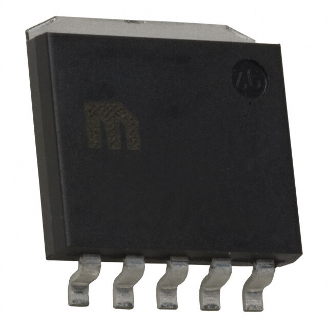
| 产品图片 |
|
| 产品型号 | TA4800AF(T6L1,Q) |
| rohs | 不受无铅要求限制 / 符合限制有害物质指令(RoHS)规范要求 |
| 产品系列 | - |
| 供应商器件封装 | 5-HSIP |
| 其它名称 | TA4800AF(T6L1Q)TR |
| 包装 | 带卷 (TR) |
| 安装类型 | 表面贴装 |
| 封装/外壳 | TO-252-6,DPak(5 引线 + 接片) |
| 工作温度 | -40°C ~ 150°C |
| 标准包装 | 2,000 |
| 特色产品 | http://www.digikey.com/cn/zh/ph/Toshiba/TA48-TA48S.html |
| 电压-跌落(典型值) | 0.69V @ 1A |
| 电压-输入 | 2.5 V ~ 16 V |
| 电压-输出 | 1.5 V ~ 9 V |
| 电流-输出 | 1A |
| 电流-限制(最小值) | 2A |
| 稳压器拓扑 | 正,可调式 |
| 稳压器数 | 1 |


- 商务部:美国ITC正式对集成电路等产品启动337调查
- 曝三星4nm工艺存在良率问题 高通将骁龙8 Gen1或转产台积电
- 太阳诱电将投资9.5亿元在常州建新厂生产MLCC 预计2023年完工
- 英特尔发布欧洲新工厂建设计划 深化IDM 2.0 战略
- 台积电先进制程称霸业界 有大客户加持明年业绩稳了
- 达到5530亿美元!SIA预计今年全球半导体销售额将创下新高
- 英特尔拟将自动驾驶子公司Mobileye上市 估值或超500亿美元
- 三星加码芯片和SET,合并消费电子和移动部门,撤换高东真等 CEO
- 三星电子宣布重大人事变动 还合并消费电子和移动部门
- 海关总署:前11个月进口集成电路产品价值2.52万亿元 增长14.8%


PDF Datasheet 数据手册内容提取
TA4800AF TOSHIBA Bipolar Linear Integrated Circuit Silicon Monolithic TA4800AF 1 A Output Current Low Dropout Voltage Regulator The TA4800AF consists of small-surface mount type low-dropout regulators with an output current of 1 A (maximum). The output voltage can be arbitrarily set by external resistance. Features HSIP5-P-1.27B • Maximum output current : 1 A Weight : 0.36 g (typ.) • Output voltage : VOUT = 1.5 V to 9.0 V • Reference voltage accuracy : VREF ± 2.5% (@Tj = 25°C) • Low quiescent current : 850 μA (typ.) (@VOUT = 3.3 V, IOUT = 0 A) • Low standby current (output OFF mode): 0.5 μA (typ.) • Low-dropout voltage : VD = 0.5 V (max) (@VOUT = 3.3 V, IOUT = 500 mA) • Protection function : Overcurrent protection / overheating protection • Package type : Surface-mount 5-pin New PW-Mold Pin Assignment Mark 1 2 3 4 5 NC IN GND OUT ADJ Start of commercial production 2005-11 1 2013-11-01
TA4800AF Marking 3 4800 Part No. (or abbreviation code) AF Lot No. Note 1 1 2 3 4 5 Note 1: A line under a Lot No. identifies the indication of product Labels. Not underlined: [[Pb]]/INCLUDES > MCV Underlined: [[G]]/RoHS COMPATIBLE or [[G]]/RoHS [[Pb]] Please contact your TOSHIBA sales representative for details as to environmental matters such as the RoHS compatibility of Product. The RoHS is the Directive 2011/65/EU of the European Parliament and of the Council of 8 June 2011 on the restriction of the use of certain hazardous substances in electrical and electronic equipment. The product(s) in this document (“Product”) contain functions intended to protect the Product from temporary small overloads such as minor short-term overcurrent or overheating. The protective functions do not necessarily protect Product under all circumstances. When incorporating Product into your system, please design the system (1) to avoid such overloads upon the Product, and (2) to shut down or otherwise relieve the Product of such overload conditions immediately upon occurrence. For details, please refer to the notes appearing below in this document and other documents referenced in this document. Pin Description Pin No. Symbol Description 1 NC Non-connection 2 IN Input terminal. Connected by capacitor (CIN) to GND. 3 GND Ground terminal 4 OUT Output terminal. Connected by capacitor (COUT) to GND. Output voltage feedback to regulator. It is connected to an error amplifier with 5 ADJ VREF=1.245 V (typ.). How to Order Product No. Package Package Type and Capacity TA4800AF (T6L1,Q) 5-pin New PW-Mold : Surface-mount Tape (2000 pcs/reel) Block Diagram IN OUT Over-current protection Over- Control ADJ temperature circuit protection Reference 1.245 V (Typ.) voltage GND 2 2013-11-01
TA4800AF Absolute Maximum Rating (Ta = 25°C) Characteristic Symbol Rating Unit Input voltage VIN 16 V Output current IOUT 1 A Operating junction temperature Tjopr -40 to 150 °C Junction temperature Tj 150 °C Storage temperature Tstg −55 to 150 °C Ta = 25°C 1 Power dissipation PD W Tc = 25°C 10 Thermal junction-ambient Rth(j-a) 125 °C/W resistance junction-case Rth(j-c) 12.5 Note 2: Do not apply current and voltage (including reverse polarity) to any pin that is not specified. Note 3: Using continuously under heavy loads (e.g. the application of high temperature/current/voltage and the significant change in temperature, etc.) may cause this product to decrease in the reliability significantly even if the operating conditions (i.e. operating temperature/current/voltage, etc.) are within the absolute maximum ratings and the operating ranges. Please design the appropriate reliability upon reviewing the Toshiba Semiconductor Reliability Handbook (“Handling Precautions”/“Derating Concept and Methods”) and individual reliability data (i.e. reliability test report and estimated failure rate, etc). Operating Input Voltage Range Characteristic Symbol Min Typ. Max Unit Input voltage VIN 2.5 (Note 4) ⎯ 16.0 V Note 4: This is the voltage at which the IC begins operating. VD must be considered when determining the best input voltage for the application. Output Voltage Range Characteristic Symbol Min Typ. Max Unit Output voltage VOUT 1.5 ⎯ 9.0 V Protection Function (Reference) Characteristic Symbol Test Condition Min Typ. Max Unit Thermal shutdown TSD 150 170 ⎯ °C VIN = 4.3 V Thermal shutdown hysteresis width TSD(hys) ⎯ 15 ⎯ °C VIN = 5.3 V, Tj = 25°C ⎯ 1.7 ⎯ Peak circuit current IPEAK A VIN = 8.3 V, Tj = 25°C ⎯ 2.0 ⎯ VIN = 5.3 V, Tj = 25°C ⎯ 1.1 ⎯ Short circuit current ISC A VIN = 16V , Tj = 25°C ⎯ 0.7 ⎯ Note 5: Ensure that the devices operate within the limits of the maximum rating when in actual use. 3 2013-11-01
TA4800AF Electrical Characteristics (Unless otherwise specified, V = V , V = 3.3 V, C = 0.33 μF, C = 3.3 μF, T = 25°C) EN IN OUT IN OUT j Characteristic Symbol Test Condition Min Typ. Max Unit Reference voltage VREF VIN = 4.3 V 1.214 1.245 1.276 V Line regulation Reg・line 4.3 V ≤ VIN ≤ 8.3 V, ⎯ 8 24 mV IOUT = 500 mA Load regulation Reg・load VIN = 4.3 V, 5 mA ≤ IOUT ≤ 1 A ⎯ 5 20 mV 4.3 V ≤ VIN ≤ 8.3 V, ⎯ 0.85 1.70 IOUT = 0 A Quiescent current IB mA 4.3 V ≤ VIN ≤ 8.3 V, ⎯ 10 20 IOUT = 1 A VIN = 2.1 V, IOUT = 0 A ⎯ 3.3 4.0 Starting quiescent current IBstart mA VIN = 3.5 V, IOUT = 1 A ⎯ 17.0 28.5 Output noise voltage VNO V10IN H =z 5≤. 3f ≤V ,1 I0O0U kTH =z 5 0 mA, ⎯ 100 ⎯ μVrms Ripple rejection R.R. VIN = 5.3 V, IOUT = 50 mA, ⎯ 63 ⎯ dB f = 120 Hz IOUT = 500 mA ⎯ 0.32 0.50 Dropout voltage VD V IOUT = 1 A ⎯ 0.69 ⎯ Acoveefrfaicgieen tte omf poeurtaptuutr ev oltage TCVO V0°INC =≤ 5T.j3 ≤ V 1,2 I5O°UCT = 5 mA, ⎯ 0.3 ⎯ mV/°C 4 2013-11-01
TA4800AF Electrical Characteristics Common to All Products • Tj = 25°C in the measurement conditions of each item is the standard condition when a pulse test is carried out, and any drift in the electrical characteristic due to a rise in the junction temperature of the chip may be disregarded. Standard Application Circuit 0.3C3IN μ F I N TA4800AOFUT R1 3C.3O UμTF ADJ GND Load R2 • Be sure to connect a capacitor near the input terminal and output terminal between both terminals and GND. The use of a monolithic ceramic capacitor (B Characteristic or X7R) of low ESR (equivalent series resistance) is recommended. The IC may oscillate due to external conditions (output current, temperature, or the type of the capacitor used). The type of capacitor required must be determined by the actual application circuit in which the IC is used. Setting Output Voltage • The output voltage is determined by the equation shown below. When you control the output voltage with R1, a recommended value to use for R2 is 5 kΩ. R1 and R2must be placed as close as possible to each other, and the board trace to the ADJ terminal must be kept as short as possible. R1 V =V × ( 1+ ) OUT REF R2 Usage Precautions • The IC might be destroyed if a voltage greater than the input terminal voltage is applied to the output terminal, or if the input terminal is connected to GND during operation. To prevent such an occurrence, connect a diode as in the following diagram. CIN IN OUT COUT 0.33 μF TA4800AF R1 3.3 μF ADJ GND Load R2 • There is a possibility that internal parasitic devices may be generated when momentary transients cause a terminal’s potential to fall below that of the GND terminal. In such case, that the device could be destroyed. The voltage of each terminal and any state must therefore never fall below the GND potential. • Low voltage Do not apply voltage to the Product that is lower than the minimum operating voltage, or the Product’s protective functions will not operate properly and the Product may be permanently damaged. 5 2013-11-01
TA4800AF • Overcurrent Protection The overcurrent protection circuits in the Product are designed to temporarily protect Product from minor overcurrent of brief duration. When the overcurrent protective function in the Product activates, immediately cease application of overcurrent to Product. Improper usage of Product, such as application of current to Product exceeding the absolute maximum ratings, could cause the overcurrent protection circuit not to operate properly and/or damage Product permanently even before the protection circuit starts to operate. • Overheating Protection The thermal shutdown circuits in the Product are designed to temporarily protect Product from minor overheating of brief duration. When the overheating protective function in the Product activates, immediately correct the overheating situation. Improper usage of Product, such as the application of heat to Product exceeding the absolute maximum ratings, could cause the overheating protection circuit not to operate properly and/or damage Product permanently even before the protection circuit starts to operate. 6 2013-11-01
TA4800AF PDmax – Ta VOUT – Tj 12 3.5 W) Condition: VIN = 5.3 V (max 10 Ta = Tc NRa eucfmelorbawem rs iooc flds IueCbr is=nt gr1a oten (V) 3.4 VOUT = 3.3V D P 8 T U n O ble power dissipatio 264 3500 mmmm ×× 3500 mmmm ×× 00..88 mmmm VOutput voltage 33..32 IOUT = 5 mA 500 m1A00 mA wa Single o All 0 3.1 0 20 40 60 80 100 120 140 160 −50 0 50 100 150 Ambient temperature Ta (°C) Junction temperature Tj (°C) VOUT – VIN IB – VIN 4 20 Tj = 25°C V) mA) ( 3 IOUT = 500 mA ( 15 OUT 10 mA 100 mA I B V nt voltage 2 nt curre 10 IOUT = 500 mA ut ce utp 1 es 5 O ui Q 100 mA 10 mA VOUT = 3.3V Tj = 25°C 0 0 0 2 4 6 8 0 2 4 6 8 Input voltage VIN (V) Input voltage VIN (V) IB – Tj IB – IOUT 30 30 VIN = 5.3 V VIN = 5.3 V Tj = 25°C A) A) m m ( ( B 20 B 20 I I urrent IOUT = 1 A urrent c c ent 10 ent 10 c c s s e e ui ui Q Q 0 A 0 0 −50 0 50 100 150 0 200 400 600 800 1000 Junction temperature Tj (°C) Output current IOUT (mA) 7 2013-11-01
TA4800AF VOUT – IOUT VOUT – IOUT 3.5 4 V) V) ( 3.4 ( 3 T T U U O O V V e 3.3 e 2 g g a a olt olt v v ut ut utp 3.2 utp 1 O VIN = 5.3 V O VIN = 5.3 V VOUT = 3.3V VOUT = 3.3V Tj = 25°C Tj = 25°C 3.1 0 0 200 400 600 800 1000 0 0.5 1 1.5 2 2.5 Output current IOUT (mA) Output current IOUT (A) VD – IOUT VD – Tj 0.8 0.8 VOUT = 3.3V VOUT = 3.3V Tj = 25°C Tj = 25°C V) Tj = −40℃ V) (D 0.6 125℃ (D 0.6 IOUT = 1 A V 85℃ V e 25℃ e ag 0.4 ag 0.4 volt volt 500 mA ut ut o o p p o 0.2 o 0.2 Dr Dr 100 mA 0 0 0 200 400 600 800 1000 −50 0 50 100 150 Output current IOUT (mA) Junction temperature Tj (°C) IPEAK – Tj IPEAK – VD 2.5 3.0 VOUT = 3.3V A) A) Tj = 25°C ( ( 2.5 2.0 K K A A E E P P 2.0 I I 1.5 nt nt urre urre 1.5 c 1.0 c put put 1.0 ut ut o o k 0.5 k a a 0.5 Pe VIN = 5.3 V Pe VOUT = 3.3V 0 0 -50 0 50 100 150 0 5 10 15 20 Junction temperature Tj (°C) Dropout voltage VD (V) 8 2013-11-01
TA4800AF Package Dimensions HSIP5-P-1.27B Unit: mm 6.5±0.2 2 0. 5.2±0.2 ± 0.6max 5 1. 2 3 0. 0. ± ± 5 5 1.1±0.2 5. 9. 2 0. ± 0.6±0.1 0.7±0.1 5 1. 0.7max 0.8max 0.6max 0.5±0.1 0.5±0.1 2 ±0. ±0.1 2.3 0.1 1.27 Weight: 0.36 g (typ.) 9 2013-11-01
TA4800AF RESTRICTIONS ON PRODUCT USE • Toshiba Corporation, and its subsidiaries and affiliates (collectively "TOSHIBA"), reserve the right to make changes to the information in this document, and related hardware, software and systems (collectively "Product") without notice. • This document and any information herein may not be reproduced without prior written permission from TOSHIBA. Even with TOSHIBA's written permission, reproduction is permissible only if reproduction is without alteration/omission. • Though TOSHIBA works continually to improve Product's quality and reliability, Product can malfunction or fail. Customers are responsible for complying with safety standards and for providing adequate designs and safeguards for their hardware, software and systems which minimize risk and avoid situations in which a malfunction or failure of Product could cause loss of human life, bodily injury or damage to property, including data loss or corruption. Before customers use the Product, create designs including the Product, or incorporate the Product into their own applications, customers must also refer to and comply with (a) the latest versions of all relevant TOSHIBA information, including without limitation, this document, the specifications, the data sheets and application notes for Product and the precautions and conditions set forth in the "TOSHIBA Semiconductor Reliability Handbook" and (b) the instructions for the application with which the Product will be used with or for. Customers are solely responsible for all aspects of their own product design or applications, including but not limited to (a) determining the appropriateness of the use of this Product in such design or applications; (b) evaluating and determining the applicability of any information contained in this document, or in charts, diagrams, programs, algorithms, sample application circuits, or any other referenced documents; and (c) validating all operating parameters for such designs and applications. TOSHIBA ASSUMES NO LIABILITY FOR CUSTOMERS' PRODUCT DESIGN OR APPLICATIONS. • PRODUCT IS NEITHER INTENDED NOR WARRANTED FOR USE IN EQUIPMENTS OR SYSTEMS THAT REQUIRE EXTRAORDINARILY HIGH LEVELS OF QUALITY AND/OR RELIABILITY, AND/OR A MALFUNCTION OR FAILURE OF WHICH MAY CAUSE LOSS OF HUMAN LIFE, BODILY INJURY, SERIOUS PROPERTY DAMAGE AND/OR SERIOUS PUBLIC IMPACT ("UNINTENDED USE"). Except for specific applications as expressly stated in this document, Unintended Use includes, without limitation, equipment used in nuclear facilities, equipment used in the aerospace industry, medical equipment, equipment used for automobiles, trains, ships and other transportation, traffic signaling equipment, equipment used to control combustions or explosions, safety devices, elevators and escalators, devices related to electric power, and equipment used in finance-related fields. IF YOU USE PRODUCT FOR UNINTENDED USE, TOSHIBA ASSUMES NO LIABILITY FOR PRODUCT. For details, please contact your TOSHIBA sales representative. • Do not disassemble, analyze, reverse-engineer, alter, modify, translate or copy Product, whether in whole or in part. • Product shall not be used for or incorporated into any products or systems whose manufacture, use, or sale is prohibited under any applicable laws or regulations. • The information contained herein is presented only as guidance for Product use. No responsibility is assumed by TOSHIBA for any infringement of patents or any other intellectual property rights of third parties that may result from the use of Product. No license to any intellectual property right is granted by this document, whether express or implied, by estoppel or otherwise. • ABSENT A WRITTEN SIGNED AGREEMENT, EXCEPT AS PROVIDED IN THE RELEVANT TERMS AND CONDITIONS OF SALE FOR PRODUCT, AND TO THE MAXIMUM EXTENT ALLOWABLE BY LAW, TOSHIBA (1) ASSUMES NO LIABILITY WHATSOEVER, INCLUDING WITHOUT LIMITATION, INDIRECT, CONSEQUENTIAL, SPECIAL, OR INCIDENTAL DAMAGES OR LOSS, INCLUDING WITHOUT LIMITATION, LOSS OF PROFITS, LOSS OF OPPORTUNITIES, BUSINESS INTERRUPTION AND LOSS OF DATA, AND (2) DISCLAIMS ANY AND ALL EXPRESS OR IMPLIED WARRANTIES AND CONDITIONS RELATED TO SALE, USE OF PRODUCT, OR INFORMATION, INCLUDING WARRANTIES OR CONDITIONS OF MERCHANTABILITY, FITNESS FOR A PARTICULAR PURPOSE, ACCURACY OF INFORMATION, OR NONINFRINGEMENT. • Do not use or otherwise make available Product or related software or technology for any military purposes, including without limitation, for the design, development, use, stockpiling or manufacturing of nuclear, chemical, or biological weapons or missile technology products (mass destruction weapons). Product and related software and technology may be controlled under the applicable export laws and regulations including, without limitation, the Japanese Foreign Exchange and Foreign Trade Law and the U.S. Export Administration Regulations. Export and re-export of Product or related software or technology are strictly prohibited except in compliance with all applicable export laws and regulations. • Please contact your TOSHIBA sales representative for details as to environmental matters such as the RoHS compatibility of Product. Please use Product in compliance with all applicable laws and regulations that regulate the inclusion or use of controlled substances, including without limitation, the EU RoHS Directive. TOSHIBA ASSUMES NO LIABILITY FOR DAMAGES OR LOSSES OCCURRING AS A RESULT OF NONCOMPLIANCE WITH APPLICABLE LAWS AND REGULATIONS. 10 2013-11-01