ICGOO在线商城 > 集成电路(IC) > PMIC - 配电开关,负载驱动器 > T6819-TBQ

 Datasheet下载
- 型号: T6819-TBQ
- 制造商: Atmel
- 库位|库存: xxxx|xxxx
- 要求:
| 数量阶梯 | 香港交货 | 国内含税 |
| +xxxx | $xxxx | ¥xxxx |
查看当月历史价格
查看今年历史价格
T6819-TBQ产品简介:
ICGOO电子元器件商城为您提供T6819-TBQ由Atmel设计生产,在icgoo商城现货销售,并且可以通过原厂、代理商等渠道进行代购。 T6819-TBQ价格参考。AtmelT6819-TBQ封装/规格:PMIC - 配电开关,负载驱动器, Power Switch/Driver 1:6 N 通道 1.5A 16-SO。您可以下载T6819-TBQ参考资料、Datasheet数据手册功能说明书,资料中有T6819-TBQ 详细功能的应用电路图电压和使用方法及教程。
| 参数 | 数值 |
| 产品目录 | 集成电路 (IC) |
| 描述 | IC DRIVER DUAL TRPL DMOS 16-SOIC |
| 产品分类 | PMIC - MOSFET,电桥驱动器 - 内部开关 |
| 品牌 | Atmel |
| 数据手册 | |
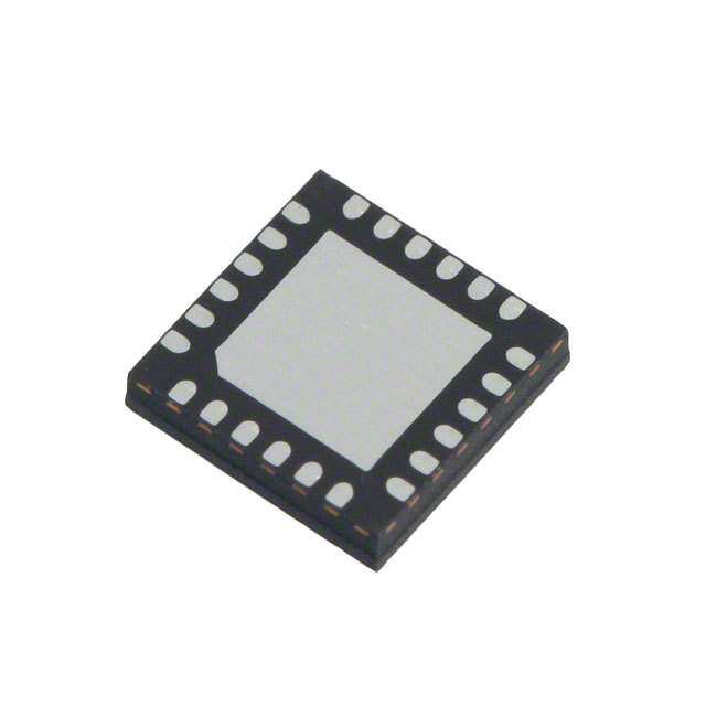
| 产品图片 |
|
| 产品型号 | T6819-TBQ |
| rohs | |
| 产品系列 | - |
| 产品目录页面 | |
| 供应商器件封装 | 16-SO |
| 其它名称 | T6819-TBQCT |
| 包装 | 剪切带 (CT) |
| 安装类型 | 表面贴装 |
| 导通电阻 | 500 毫欧 |
| 封装/外壳 | 16-SOIC(0.154",3.90mm 宽) |
| 工作温度 | -40°C ~ 150°C |
| 标准包装 | 1 |
| 电压-电源 | 7 V ~ 40 V |
| 电流-峰值输出 | 2A |
| 电流-输出/通道 | 1.5A |
| 类型 | 高端/低端驱动器 |
| 输入类型 | 串行 |
| 输出数 | 6 |
| 配用 | /product-detail/zh/ATAB6819/ATAB6819-ND/1027019 |


- 商务部:美国ITC正式对集成电路等产品启动337调查
- 曝三星4nm工艺存在良率问题 高通将骁龙8 Gen1或转产台积电
- 太阳诱电将投资9.5亿元在常州建新厂生产MLCC 预计2023年完工
- 英特尔发布欧洲新工厂建设计划 深化IDM 2.0 战略
- 台积电先进制程称霸业界 有大客户加持明年业绩稳了
- 达到5530亿美元!SIA预计今年全球半导体销售额将创下新高
- 英特尔拟将自动驾驶子公司Mobileye上市 估值或超500亿美元
- 三星加码芯片和SET,合并消费电子和移动部门,撤换高东真等 CEO
- 三星电子宣布重大人事变动 还合并消费电子和移动部门
- 海关总署:前11个月进口集成电路产品价值2.52万亿元 增长14.8%


PDF Datasheet 数据手册内容提取
Features (cid:127) Supply Voltage up to 40V (cid:127) R Typically 0.5Ω at 25°C, Maximum1.1Ω at 150°C DSon (cid:127) Up to 1.5A Output Current (cid:127) Three High-side and Three Low-side Drivers Usable as Single Outputs or Half Bridges (cid:127) Capable to Switch all Kinds of Loads such as DC Motors, Bulbs, Resistors, Capacitors and Inductors (cid:127) PWM Capability for Each Output Controlled by External PWM Signal (cid:127) No Shoot-through Current (cid:127) Very Low Quiescent Current I < 5µA in Standby Mode over Total Temperature Range S (cid:127) Outputs Short-circuit Protected Dual Triple (cid:127) Selective Overtemperature Protection for Each Switch and Overtemperature Prewarning DMOS Output (cid:127) Undervoltage Protection (cid:127) Various Diagnostic Functions such as Shorted Output, Open Load, Overtemperature Driver with and Power-supply Fail Detection (cid:127) Serial Data Interface, Daisy Chain Capable, up to 2MHz Clock Frequency Serial Input (cid:127) SO16 Power Package Control Description T6819/T6829 The T6819/T6829 are fully protected driver interfaces designed in 0.8-µm BCDMOS technology. They are used to control up to six different loads by a microcontroller in automotive and industrial applications. Each of the three high-side and three low-side drivers is capable to drive currents up to 1.5A. Each driver is freely configurable and can be controlled separately from a Preliminary standard serial data interface. Therefore, all kinds of loads such as bulbs, resistors, capacitors and inductors can be combined. The IC design especially supports the applications of H-bridges to drive DC motors. The capability to control each output with an external PWM signal opens additional applications. Protection is guaranteed regarding short-circuit conditions, overtemperature and und- ervoltage. Various diagnostic functions and a very low quiescent current in stand-by mode opens a wide range of applications. Automotive qualification (protection against conducted interferences, EMC protection and 2-kV ESD protection) gives added value and enhanced quality for exacting requirements of automotive applications. Rev.4531D–BCD–07/04
Figure 1. Block Diagram OUT3H OUT2H OUT1H 4 14 13 Charge pump Fault Fault Fault detect detect detect 6 12 VS DI O O P P P P P P H L H L H L S 7 S C L H L H L H L S S S S S S R CLK I S D 3 3 2 2 1 1 3 3 2 2 1 1 R UV - Control protection Input register Serial interface logic 5 Output register Power-on 11 VCC CS reset P I O n. n. n. n. n. n. H L H L H L T S N V u. u. u. u. u. u. S S S S S S P F H L 3 3 2 2 1 1 10 DO 16 GND 8 PWM Thermal Fault Fault Fault protection 9 detect detect detect GND 1 GND 3 15 2 OUT3L OUT2L OUT1L T6819/T6829 [Preliminary] 2 4531D–BCD–07/04
T6819/T6829 [Preliminary] Pin Configuration Figure 2. Pinning SO16 GND 1 16 GND OUT1L 2 15 OUT2L OUT3L 3 14 OUT2H OUT3H 4 13 OUT1H CS 5 12 VS DI 6 11 VCC CLK 7 10 DO PWM 8 9 GND Pin Description Pin Symbol Function T6819: ground; reference potential; internal connection to pin 9 and pin 16; cooling tab 1 GND T6829: additional connection to heat slug Low-side driver output 1; power MOS open drain with internal reverse diode; short-circuit protection; 2 OUT1L overtemperature protection; diagnosis for short and open load; PWM ability 3 OUT3L Low-side driver output 3; see pin 2 High-side driver output 3; power MOS open source with internal reverse diode; short-circuit protection; 4 OUT3H overtemperature protection; diagnosis for short and open load; PWM ability Chip select input; 5-V CMOS logic level input with internal pull up; 5 CS low = serial communication is enabled, high = disabled Serial data input; 5-V CMOS logic level input with internal pull down; receives serial data from the control 6 DI device; DI expects a 16-bit control word with LSB being transferred first Serial clock input; 5-V CMOS logic level input with internal pull down; 7 CLK controls serial data input interface and internal shift register (f = 2MHz) max PWM input; 5-V CMOS logic level input with internal pull down; receives PWM signal to control outputs 8 PWM which are selected for PWM mode by the serial data interface, high = outputs on, low = outputs off 9 GND Ground; see pin 1 Serial data output; 5-V CMOS logic-level tri-state output for output (status) register data; sends 16-bit 10 DO status information to the microcontroller (LSB is transferred first); output will remain tri-stated unless device is selected by CS = low, therefore, several ICs can operate on one data-output line only. 11 VCC Logic supply voltage (5V) 12 VS Power supply for high-side output stages OUT1H, OUT2H, OUT3H, internal supply 13 OUT1H High-side driver output 1; see pin 4 14 OUT2H High-side driver output 2; see pin 4 15 OUT2L Low-side driver output 2; see pin 2 16 GND Ground; see pin 1 3 4531D–BCD–07/04
Functional Description Serial Interface Data transfer starts with the falling edge of the CS signal. Data must appear at DI syn- chronized to CLK and are accepted on the falling edge of the CLK signal. LSB (bit 0, SRR) has to be transferred first. Execution of new input data is enabled on the rising edge of the CS signal. When CS is high, pin DO is in tri-state condition. This output is enabled on the falling edge of CS. Output data will change their state with the rising edge of CLK and stay stable until the next rising edge of CLK appears. LSB (bit 0, TP) is transferred first. Figure 3. Data Transfer CS DI SRR LS1 HS1 LS2 HS2 LS3 HS3 PL1 PH1 PL2 PH2 PL3 PH3 OLD OCS SI 0 1 2 3 4 5 6 7 8 9 10 11 12 13 14 15 CLK DO TP S1L S1H S2L S2H S3L S3H n. u. n. u. n. u. n. u. n. u. n. u. OVL INH PSF Table 1. Input Data Protocol Bit Input Register Function Status register reset (high = reset; the bits PSF and OVL in the 0 SRR output data register are set to low) 1 LS1 Controls output LS1 (high = switch output LS1 on) 2 HS1 Controls output HS1 (high = switch output HS1 on) 3 LS2 See LS1 4 HS2 See HS1 5 LS3 See LS1 6 HS3 See HS1 7 PL1 Output LS1 additionally controlled by PWM Input 8 PH1 Output HS1 additionally controlled by PWM Input 9 PL2 See PL1 10 PH2 See PH1 11 PL3 See PL1 12 PH3 See PH1 13 OLD Open load detection (low = on) 14 OCS Overcurrent shutdown (high = overcurrent shutdown is active) Software inhibit; low = standby, high = normal operation 15 SI (data transfer is not affected by standby function because the digital part is still powered) T6819/T6829 [Preliminary] 4 4531D–BCD–07/04
T6819/T6829 [Preliminary] Table 2. Output Data Protocol Output (Status) Bit Register Function 0 TP Temperature prewarning: high = warning Normal operation: high = output is on, low = output is off Open-load detection: high = open load, low = no open load 1 Status LS1 (correct load condition is detected if the corresponding output is switched off); not affected by SRR Normal operation: high = output is on, low = output is off Open-load detection: high = open load, low = no open load 2 Status HS1 (correct load condition is detected if the corresponding output is switched off); not affected by SRR 3 Status LS2 Description see LS1 4 Status HS2 Description see HS1 5 Status LS3 Description see LS1 6 Status HS3 Description see HS1 7 n. u. Not used 8 n. u. Not used 9 n. u. Not used 10 n. u. Not used 11 n. u. Not used 12 n. u. Not used Over-load detected: set high, when at least one output is switched off by a short-circuit condition or an overtemperature event. Bits 1 13 OVL to 6 can be used to detect the affected switch. (open-load detection bit OLD = high) Inhibit: this bit is controlled by software (bit SI in input register) 14 INH High = standby, low = normal operation 15 PSF Power-supply fail: undervoltage at pin VS detected After power-on reset, the input register has the following status: Bit 15 Bit 14 Bit 13 Bit 12 Bit 11 Bit 10 Bit 9 Bit 8 Bit 7 Bit 6 Bit 5 Bit 4 Bit 3 Bit 2 Bit 1 Bit 0 SI OCS OLD PH3 PL3 PH2 PL2 PH1 PL1 HS3 LS3 HS2 LS2 HS1 LS1 SRR H H H L L L L L L L L L L L L L The following patterns are used to enable internal test modes of the IC. It is not recommended to use these patterns during normal operation. Bit 15 Bit 14 Bit 13 Bit 12 Bit 11 Bit 10 Bit 9 Bit 8 Bit 7 Bit 6 Bit 5 Bit 4 Bit 3 Bit 2 Bit 1 Bit 0 (OCS) (HS3) (LS3) (HS2) (LS2) (HS1) (LS1) (SRR) H H H H H L L L L L L L L L L L H H H L L H H L L L L L L L L L H H H L L L L H H L L L L L L L 5 4531D–BCD–07/04
Power-supply Fail In case of undervoltage at pin VS, the Power-Supply Fail bit (PSF) in the output register is set and all outputs are disabled. To detect an undervoltage, its duration has to last longer than the undervoltage detection delay time t . The outputs are enabled immedi- dUV ately when supply voltage recovers normal operation value. The PSF bit stays high until it is reset by the SRR bit in the input register. Open-load Detection If the open-load detection bit (OLD) is set to low, a pull-up current for each high-side switch and a pull-down current for each low-side switch is turned on (open-load detec- tion current I ). If the current through the external load does not reach the open- OUT1-3 load detection current, the corresponding bit of the output in the output register is set to high. Switching on an output stage with OLD bit set to low disables the open-load function for this output. Overtemperature If the junction temperature of one ore more output stages exceeds the thermal prewarn- Protection ing threshold, T , the temperature prewarning bit (TP) in the output register is set. jPW set When the temperature falls below the thermal prewarning threshold, T , the bit TP jPW reset is reset. The TP bit can be read without transferring a complete 16-bit data word. The status of TP is available at pin DO with the falling edge of CS. After the microcontroller has read this information, CS is set high and the data transfer is interrupted without affecting the status of input and output registers. If the junction temperature of an output stage exceeds the thermal shutdown threshold, T , the affected output is disabled and the corresponding bit in the output register j switch off is set to low. Additional the overload detection bit (OVL) in the output register is set. The output can be enabled again when the temperature falls below the thermal shutdown threshold, T and the SRR bit in the input register is set to high. Hysteresis of ther- jswitch on mal prewarning and shutdown threshold avoids oscillations. Short-circuit Protection The output currents are limited by a current regulator. Overcurrent detection is activated by writing a high to the OCS bit in the input register. When the current in an output stage exceeds the overcurrent limitation and shut-down threshold, it is switched off after a delay time (t ). The over-load detection bit (OVL) is set and the corresponding status dSd bit in the output register is set to low. For OCS = low the overcurrent shutdown is inac- tive and the OVL bit is not set by an overcurrent. By writing a high to the SRR bit in the input register the OVL bit is reset and the disabled outputs are enabled. Inhibit The SI bit in the input register has to be set to zero to inhibit the T6819/T6829. All output stages are then turned off but the serial interface stays active. The current consumption is reduced to less than 5µA at pin VS and less than 100µA at pin VCC. The output stages can be activated again by bit SI = 1. T6819/T6829 [Preliminary] 6 4531D–BCD–07/04
T6819/T6829 [Preliminary] Absolute Maximum Ratings Stresses beyond those listed under “Absolute Maximum Ratings” may cause permanent damage to the device. This is a stress rating only and functional operation of the device at these or any other conditions beyond those indicated in the operational sections of this specification is not implied. Exposure to absolute maximum rating conditions for extended periods may affect device reliability. All values refer to GND pins. Parameters Pin Symbol Value Unit Supply voltage 12 V -0.3 to +40 V VS Supply voltage 12 V -1 V t < 0.5 s; I > -2 A VS S Logic supply voltage 11 V -0.3 to +7 V VCC Logic input voltage 5 to 8 V , V , V , V -0.3 to V + 0.3 V CS DI CLK PWM VCC Logic output voltage 10 V -0.3 to V + 0.3 V DO VCC Input current 5 to 8 I , I , I ,I -10 to +10 mA CS DI CLK PWM Output current 10 I -10 to +10 mA DO 2 to 4 I , I I Output current Out3H Out2H, Out1H Internally limited, see output specification 13 to 15 I , I I Out3L Out2L, Out1L 2 to 4 I , I I Output voltage Out3H Out2H, Out1H -0.3 to +40 V 13 to 15 I , I I Out3L Out2L, Out1L 2 to 4 Reverse conducting current I , I I 13 to 15 Out3H Out2H, Out1H 17 A (t = 150 µs) I , I I pulse towards pin 12 Out3L Out2L, Out1L Junction temperature range T -40 to +150 °C J Storage temperature range T -55 to +150 °C STG Thermal Resistance Parameters Test Conditions Symbol Value Unit T6819 Measured to GND Junction pin R 30 K/W Pins 1, 9 and 16 thJP Junction ambient R 65 K/W thJA T6829 Measured to heat slug Junction pin R 5 K/W GND pins 1, 9 and 16 thJP Junction ambient R 30 K/W thJA Operating Range Parameters Symbol Value Unit Supply voltage V V (1) to 40 V VS UV Logic supply voltage V 4.75 to 5.25 V VCC Logic input voltage V ,V , V ,V -0.3 to V V CS DI CLK PWM VCC Serial interface clock frequency f 2 MHz CLK PWM input frequency f 1 kHz PWM Junction temperature range T -40 to +150 °C j Note: 1. Threshold for undervoltage detection. 7 4531D–BCD–07/04
Noise and Surge Immunity Parameters Test Conditions Value Conducted interferences ISO 7637-1 Level 4(1) Interference suppression VDE 0879 Part 2 Level 5 ESD (Human Body Model) ESD S 5.1 2 kV ESD (Machine Model) JEDEC A115A 200 V Note: 1. Test pulse 5: V = 40 V. smax Electrical Characteristics 7.5V < V < 40V; 4.75V < V < 5.25V; INH = High; -40°C < T < 150°C; unless otherwise specified, all values refer to GND pins. S CC j No. Parameters Test Conditions Pin Symbol Min. Typ. Max. Unit Type* 1 Current Consumption 1.1 Quiescent current VS V < 20V, SI = low 12 I 1 5 µA A VS VS 4.75V < V < 5.25V, 1.2 Quiescent current VCC VCC 11 I 60 100 µA A SI = low VCC V < 20V normal VS operating, all outputs 1.3 Supply current VS 12 I 4 6 mA A off, input register bit 13 VS (OLD) = high 4.75V < V < 5.25V, 1.4 Supply current VCC VCC 11 I 350 650 µA A normal operating VCC 1.5 Discharge current VS V = 32.5V, INH = low 12 I 0.5 5.5 mA A VS VS 1.6 Discharge current VS V = 40V, INH = low 12 I 2.5 10 mA A VS VS 2 Undervoltage Detection, Power-on Reset Power-on reset 2.1 11 V 3.2 3.9 4.4 V A threshold VCC Power-on reset delay 2.2 After switching on V t 30 95 190 µs A time CC dPor Undervoltage-detection 2.3 V =5V 12 V 5.6 7.0 V A threshold CC Uv Undervoltage-detection 2.4 V = 5V 12 ∆V 0.6 V A hysteresis CC Uv Undervoltage-detection 2.5 t 10 40 µs A delay time dUV 3 Thermal Prewarning and Shutdown 3.1 Thermal prewarning set T 120 145 170 °C B jPW set Thermal prewarning 3.2 T 105 130 155 °C B reset jPW reset Thermal prewarning 3.3 ∆T 15 K B hysteresis jPW 3.4 Thermal shutdown off T 150 175 200 °C B j switch off *) Type means: A =100% tested, B = 100% correlation tested, C = Characterized on samples, D = Design parameter Note: 1. Delay time between rising edge of input signal at pin CS after data transmission and switch on/off output stages to 90% of final level. Device not in standby for t > 1 ms. 2. Delay time between rising/falling edge of input signal at pin PWM and switch on/off output stages to 90% of final level. 3. Difference between switch-on and switch-off delay time of input signal at pin PWM to output stages in PWM mode. T6819/T6829 [Preliminary] 8 4531D–BCD–07/04
T6819/T6829 [Preliminary] Electrical Characteristics (Continued) 7.5V < V < 40V; 4.75V < V < 5.25V; INH = High; -40°C < T < 150°C; unless otherwise specified, all values refer to GND pins. S CC j No. Parameters Test Conditions Pin Symbol Min. Typ. Max. Unit Type* 3.5 Thermal shutdown on T 135 160 185 °C B j switch on Thermal shutdown 3.6 ∆T 15 K B hysteresis j switch off Ratio thermal shutdown T 3.7 off/thermal prewarning j switch off/ 1.05 1.2 B T set jPW set Ratio thermal shutdown T 3.8 on/thermal prewarning j switch on/ 1.05 1.2 B T reset jPW reset 4 Output Specification (OUT1-OUT3) 4, 13, 4.1 I = -1.3A R 1.1 Ω A On resistance Out 1-3 H 14 DSOn1-3H 4.2 I = 1.3A 2, 3, 15 R 1.1 Ω A Out 1-3 L DSOn1-3L High-side output V = 0V 4, 13, 4.3 Out 1-3 H , I -5 µA A leakage current output stages off 14 Out1-3H Low-side output V = V 4.4 Out 1-3 L VS, 2, 3, 15 I 5 µA A leakage current output stages off Out1-3L High-side switch 4, 13, 4.5 reverse diode forward I = 1.5A V - V 1.5 V A Out 14 Out1-3 VS voltage Low-side switch 4.6 reverse diode forward I = -1.5A 2, 3, 15 V -1.5 V A Out 1-3 L Out1-3L voltage High-side overcurrent 4, 13, 4.7 limitation and shutdown I -2.5 -2 -1.5 A A 14 Out1-3H threshold Low-side overcurrent 4.8 limitation and shutdown 2, 3, 15 I 1.5 2 2.5 A A Out1-3L threshold Overcurrent shutdown 4.9 t 10 40 µs A delay time dSd High-side open load Input register bit 13 4, 13, 4.10 I -2.5 -0.2 mA A detection current (OLD) = low, output off 14 Out1-3H Low-side open load Input register bit 13 4.11 2, 3, 15 I 0.2 2.5 mA A detection current (OLD) = low, output off Out1-3L High-side output switch V = 13V 4.12 VS t 20 µs A on delay(1),(2) R =30Ω don Load Low-side output switch V = 13V 4.13 VS t 20 µs A on delay(1),(2) R =30Ω don Load High-side output switch V =13V 4.14 VS t 20 µs A off delay(1),(2) R = 30Ω doff Load *) Type means: A =100% tested, B = 100% correlation tested, C = Characterized on samples, D = Design parameter Note: 1. Delay time between rising edge of input signal at pin CS after data transmission and switch on/off output stages to 90% of final level. Device not in standby for t > 1 ms. 2. Delay time between rising/falling edge of input signal at pin PWM and switch on/off output stages to 90% of final level. 3. Difference between switch-on and switch-off delay time of input signal at pin PWM to output stages in PWM mode. 9 4531D–BCD–07/04
Electrical Characteristics (Continued) 7.5V < V < 40V; 4.75V < V < 5.25V; INH = High; -40°C < T < 150°C; unless otherwise specified, all values refer to GND pins. S CC j No. Parameters Test Conditions Pin Symbol Min. Typ. Max. Unit Type* Low-side output switch V =13V 4.15 VS t 3 µs A off delay(1),(2) R = 30Ω doff Load Dead time between V =13V 4.16 corresponding high- VS t - t 1 µs A R = 30 Ω don doff and low-side switches Load ∆t V = 13V ∆t 4.17 dPWM VS dPWM = 20 µs A low-side switch(3) R = 30Ω t - t Load don doff ∆t V = 13V ∆t 4.18 dPWM VS dPWM = 3 7 µs A high-side switch(3) R = 30Ω t - t Load don doff 5 Logic Inputs DI, CLK, CS, PWM Input voltage low-level 0.3 × 5.1 5-8 V V A threshold IL V VCC Input voltage high-level 0.7 × 5.2 5-8 V V A threshold IH V VCC Hysteresis of input 5.3 5-8 ∆V 50 700 mV A voltage I Pull-down current 5.4 V , V V = V 6, 7, 8 I 10 65 µA A Pins DI, CLK, PWM DI CLK, PWM CC PD Pull-up current 5.5 V = 0V 5 I -65 -10 µA A Pin CS CS PU 6 Serial Interface – Logic Output DO Output-voltage low 6.1 I = 2mA 10 V 0.4 V A level DOL DOL Output-voltage high V - 6.2 I = -2mA 10 V VCC V A level DOL DOH 0.7V Leakage current V = V 6.3 CS CC 10 I -10 10 µA A (tri-state) 0V < V < V DO DO VCC 7 Inhibit Input – Timing Delay time from 7.1 standby to normal t 100 µs A dINH operation *) Type means: A =100% tested, B = 100% correlation tested, C = Characterized on samples, D = Design parameter Note: 1. Delay time between rising edge of input signal at pin CS after data transmission and switch on/off output stages to 90% of final level. Device not in standby for t > 1 ms. 2. Delay time between rising/falling edge of input signal at pin PWM and switch on/off output stages to 90% of final level. 3. Difference between switch-on and switch-off delay time of input signal at pin PWM to output stages in PWM mode. T6819/T6829 [Preliminary] 10 4531D–BCD–07/04
T6819/T6829 [Preliminary] Serial Interface – Timing No. Parameters Test Conditions Pin Timing Chart No.(1) Symbol Min. Typ. Max. Unit Type* DO enable after CS 8.1 C = 100 pF 10 1 t 200 ns D falling edge DO ENDO DO disable after CS 8.2 C = 100 pF 10 2 t 200 ns D rising edge DO DISDO 8.3 DO fall time C = 100 pF 10 - t 100 ns D DO DOf 8.4 DO rise time C = 100 pF 10 - t 100 ns D DO DOr 8.5 DO valid time C = 100 pF 10 10 t 200 ns D DO DOVal 8.6 CS setup time 5 4 t 225 ns D CSSethl 8.7 CS setup time 5 8 t 225 ns D CSSetlh 8.8 CS high time 5 9 t 500 ns D CSh 8.9 CLK high time 7 5 t 225 ns D CLKh 8.10 CLK low time 7 6 t 225 ns D CLKl 8.11 CLK period time 7 - t 500 ns D CLKp 8.12 CLK setup time 7 7 t 225 ns D CLKSethl 8.13 CLK setup time 7 3 t 225 ns D CLKSetlh 8.14 DI setup time 6 11 t 40 ns D DIset 8.15 DI hold time 6 12 t 40 ns D DIHold *) Type means: A =100% tested, B = 100% correlation tested, C = Characterized on samples, D = Design parameter Note: 1. See Figure 4 on page 12 11 4531D–BCD–07/04
Figure 4. Serial Interface Timing with Chart Number 1 2 CS DO 9 CS 4 7 CLK 5 3 6 8 DI 11 CLK 10 12 DO Inputs DI, CLK, CS: High level = 0.7 × V , low level = 0.3 × V CC CC Output DO: High level = 0.8 × V , low level = 0.2 × V CC CC T6819/T6829 [Preliminary] 12 4531D–BCD–07/04
T6819/T6829 [Preliminary] Application Circuit V CC U5021M M M Watchdog OUT3H OUT2H OUT1H Reset Trigger 4 14 13 Cphuamrgpe VS Fault Fault Fault detect detect detect V 6 12 VS Batt DI 0 to 40 V + O O P P P P P P H L H L H L S er CLK 7 SI CS DL H3 L3 H2 2L H1 L1 S3 S3 S2 S2 S1 S1 RR l UV - ontrol CS 5 InOpuutt preugt irsetgeirster Serial interface Cloongtircol pProorwteesecert-itoonn 11 VCC V5C VC c SP NI OV nu.. nu.. nu.. nu.. nu.. nu.. SH SL HS SL HS SL TP ++ o F H L 3 3 2 2 1 1 r 10 c DO i M 16 GND 8 PWM Thermal dFeateucltt dFeateucltt dFeateucltt protection 9 GND 1 GND 3 15 2 OUT3L OUT2L OUT1L V CC Application Notes It is strongly recommended to connect the blocking capacitors at V and V as close as CC S possible to the power supply and GND pins. Recommended value for capacitors at V : S Electrolytic capacitor C > 22µF in parallel with a ceramic capacitor C = 100nF. Value for electrolytic capacitor depends on external loads, conducted interferences and reverse conducting current I (see “Absolute Maximum Ratings” on page 7). Out1,2,3 Recommended value for capacitors at V : CC Electrolytic capacitor C > 10µF in parallel with a ceramic capacitor C = 100nF. To reduce thermal resistance it is recommended to place cooling areas on the PCB as close as possible to the GND pins. Negative spikes at the output pins (e.g. negative spikes caused by an inductive load switched off with a high side driver) may activate the overtemperature protection func- tion of the T6819/T6829. In this condition, the affected output will be switched off. If this behavior is not acceptable or compatible with the specific application functionally, it is necessary, that for switching on required outputs again, the SRR bit (Status Register Reset) is set, to ensure a reset of the overtemperature function. 13 4531D–BCD–07/04
Ordering Information Extended Type Number Package Remarks T6819-TBS SO16 Power package, tubed T6819-TBQ SO16 Power package, taped and reeled T6829-T3S SO16 Power package with heat slug, tubed T6829-T3Q SO16 Power package with heat slug, taped and reeled Package Information Package SO16 5.2 4.8 Dimensions in mm 10.0 9.85 3.7 1.4 0.2 0.25 0.4 3.8 0.10 1.27 6.15 8.89 5.85 16 9 technical drawings according to DIN specifications 1 8 T6819/T6829 [Preliminary] 14 4531D–BCD–07/04
T6819/T6829 [Preliminary] Revision History Please note that the following page numbers referred to in this section refer to the specific revision mentioned, not to this document. Changes from Rev. 1. Table “Ordering Information” on page 14 changed. 4531C - 04/04 to Rev. 4531D - 07/04 15 4531D–BCD–07/04
Atmel Corporation Atmel Operations 2325 Orchard Parkway Memory RF/Automotive San Jose, CA 95131, USA 2325 Orchard Parkway Theresienstrasse 2 Tel: 1(408) 441-0311 San Jose, CA 95131, USA Postfach 3535 Fax: 1(408) 487-2600 Tel: 1(408) 441-0311 74025 Heilbronn, Germany Fax: 1(408) 436-4314 Tel: (49) 71-31-67-0 Fax: (49) 71-31-67-2340 Regional Headquarters Microcontrollers Europe 2325 Orchard Parkway 1150 East Cheyenne Mtn. Blvd. San Jose, CA 95131, USA Colorado Springs, CO 80906, USA Atmel Sarl Tel: 1(408) 441-0311 Tel: 1(719) 576-3300 Route des Arsenaux 41 Case Postale 80 Fax: 1(408) 436-4314 Fax: 1(719) 540-1759 CH-1705 Fribourg La Chantrerie Biometrics/Imaging/Hi-Rel MPU/ Switzerland BP 70602 High Speed Converters/RF Datacom Tel: (41) 26-426-5555 Fax: (41) 26-426-5500 44306 Nantes Cedex 3, France Avenue de Rochepleine Tel: (33) 2-40-18-18-18 BP 123 Asia Fax: (33) 2-40-18-19-60 38521 Saint-Egreve Cedex, France Room 1219 Tel: (33) 4-76-58-30-00 Chinachem Golden Plaza ASIC/ASSP/Smart Cards Fax: (33) 4-76-58-34-80 Zone Industrielle 77 Mody Road Tsimshatsui 13106 Rousset Cedex, France East Kowloon Tel: (33) 4-42-53-60-00 Hong Kong Fax: (33) 4-42-53-60-01 Tel: (852) 2721-9778 Fax: (852) 2722-1369 1150 East Cheyenne Mtn. Blvd. Japan Colorado Springs, CO 80906, USA 9F, Tonetsu Shinkawa Bldg. Tel: 1(719) 576-3300 1-24-8 Shinkawa Fax: 1(719) 540-1759 Chuo-ku, Tokyo 104-0033 Japan Scottish Enterprise Technology Park Tel: (81) 3-3523-3551 Maxwell Building Fax: (81) 3-3523-7581 East Kilbride G75 0QR, Scotland Tel: (44) 1355-803-000 Fax: (44) 1355-242-743 Literature Requests www.atmel.com/literature Disclaimer: Atmel Corporation makes no warranty for the use of its products, other than those expressly contained in the Company’s standard warranty which is detailed in Atmel’s Terms and Conditions located on the Company’s web site. The Company assumes no responsibility for any errors which may appear in this document, reserves the right to change devices or specifications detailed herein at any time without notice, and does not make any commitment to update the information contained herein. No licenses to patents or other intellectual property of Atmel are granted by the Company in connection with the sale of Atmel products, expressly or by implication. Atmel’s products are not authorized for use as critical components in life support devices or systems. © Atmel Corporation 2004. All rights reserved. Atmel® and combinations thereof are the registered trademarks of Atmel Corporation or its subsidiaries. Other terms and product names may be the trademarks of others. Printed on recycled paper. 4531D–BCD–07/04