ICGOO在线商城 > T488R227M004AAE2K0
 Datasheet下载
- 型号: T488R227M004AAE2K0
- 制造商: Kemet
- 库位|库存: xxxx|xxxx
- 要求:
| 数量阶梯 | 香港交货 | 国内含税 |
| +xxxx | $xxxx | ¥xxxx |
查看当月历史价格
查看今年历史价格
T488R227M004AAE2K0产品简介:
ICGOO电子元器件商城为您提供T488R227M004AAE2K0由Kemet设计生产,在icgoo商城现货销售,并且可以通过原厂、代理商等渠道进行代购。 提供T488R227M004AAE2K0价格参考以及KemetT488R227M004AAE2K0封装/规格参数等产品信息。 你可以下载T488R227M004AAE2K0参考资料、Datasheet数据手册功能说明书, 资料中有T488R227M004AAE2K0详细功能的应用电路图电压和使用方法及教程。
| 参数 | 数值 |
| 产品目录 | |
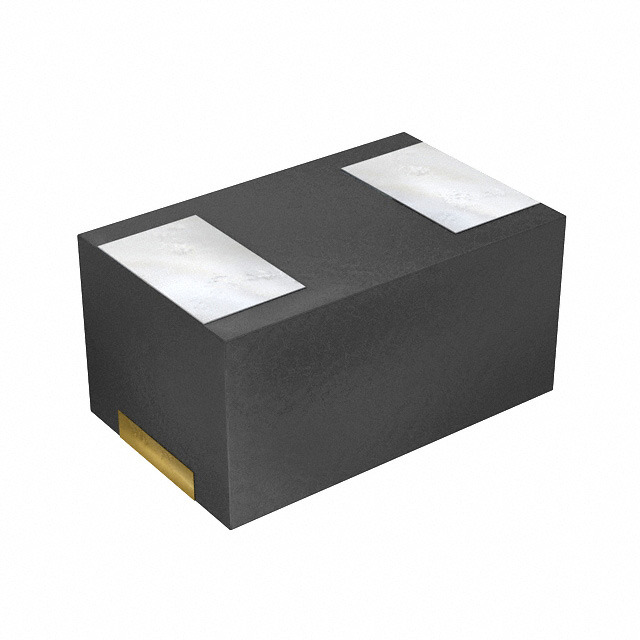
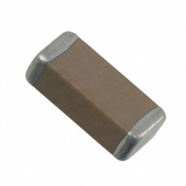
| 描述 | CAP TANT 220UF 4V 20% 2012-12钽质电容器-固体SMD 4volts 220uF 20% ESR=2000mohms |
| ESR | 2 Ohms |
| ESR(等效串联电阻) | 2 欧姆 |
| 产品分类 | |
| 品牌 | Kemet |
| 产品手册 | http://www.kemet.com/docfinder?Partnumber=T488R227M004AAE2K0 |
| 产品图片 |
|
| rohs | 符合RoHS无铅 / 符合限制有害物质指令(RoHS)规范要求 |
| 产品系列 | 钽电容器,钽质电容器-固体SMD,Kemet T488R227M004AAE2K0T488 |
| 数据手册 | http://www.kemet.com/docfinder?Partnumber=T488R227M004AAE2K0 |
| 产品型号 | T488R227M004AAE2K0 |
| 不同温度时的使用寿命 | - |
| 产品 | Tantalum Solid Surface Mounts |
| 产品种类 | 钽质电容器-固体SMD |
| 其它名称 | 399-10525-2 |
| 制造商尺寸代码 | R |
| 制造商库存号 | R Case |
| 包装 | 带卷 (TR) |
| 商标 | Kemet |
| 外壳代码-in | 0805 |
| 外壳代码-mm | 2012 |
| 外壳宽度 | 1.35 mm |
| 外壳长度 | 2 mm |
| 大小/尺寸 | 0.079" 长x 0.053" 宽(2.00mm x 1.35mm) |
| 安装类型 | 表面贴装 |
| 容差 | ±20% |
| 封装 | Reel |
| 封装/外壳 | 0805(2012 公制) |
| 封装/箱体 | 0805 (2012 metric) |
| 工作温度 | -55°C ~ 125°C |
| 工作温度范围 | - 55 C to + 125 C |
| 工厂包装数量 | 3000 |
| 引线间距 | - |
| 损耗因数DF | 6 |
| 标准包装 | 3,000 |
| 漏泄电流 | 88 uA |
| 特性 | 通用 |
| 特色产品 | http://www.digikey.cn/product-highlights/zh/t488-series-tantalum-surface-mount-capacitor/50487 |
| 电压-额定 | 4V |
| 电压额定值 | 4 V |
| 电压额定值DC | 4 V |
| 电容 | 220 uF |
| 端接类型 | SMD/SMT |
| 类型 | 模制 |
| 系列 | T488, GSV |
| 纹波电流 | 224 mA |
| 零件号别名 | TEGSVP10G227M8RKT |
| 高度 | 1.2 mm |
| 高度-安装(最大值) | 0.047"(1.20mm) |


PDF Datasheet 数据手册内容提取
Tantalum Surface Mount Capacitors – Standard Tantalum T488 Series Small Case Size Substrate Terminal MnO 2 Overview The T488 Series uses a substrate termination design, which (2.0 mm (L) x 1.2 mm (W) x 1.2 mm (H)) package size. The T488 results in one of the highest volumetric efficient packaging Series is ideal for use in densely populated circuits such as smart technologies available today in Tantalum Chip Capacitors. This phones and digital cameras where space restrictions do not allow series offers high capacitance values in the small EIA 2012-12 for larger and more commonly available case sizes. Benefits • Tantalum Technology • Substrate Termination • EIA Case Size 2012 (0805 MLCC Equivalent) • Low Profile: 1.2 mm maximum • Improved Volumetric Efficiency • Use up to 80% of rated voltage (20% derating) • Capacitance: 220 µF • Voltage: 4 V • RoHS Compliant and Halogen Free • 125°C maximum temperature capability • Lead free 260°C reflow capable • MSL Reflow Temp ≤ 260ºC = 1 Applications Typical applications include densely populated circuits where space restrictions do not allow for larger and more commonly available case sizes such as smart phones, digital cameras, MP3 players, GPS navigation systems, WiFi modules, analytical and test equipment, and audio/sound circuits. Environmental Compliance RoHS Compliant (6/6) according to Directive 2002/95/EC. Halogen free. One world. One KEMET © KEMET Electronics Corporation • P.O. Box 5928 • Greenville, SC 29606 (864) 963-6300 • www.kemet.com T2068_T488 • 6/12/2014 1
Tantalum Surface Mount Capacitors – Standard Tantalum T488 Series Small Case Size Substrate Terminal MnO 2 Ordering Information T 488 R 227 M 004 A A E2K0 Capacitor Case Capacitance Failure Rate/ Series Capacitance Code (pF) Voltage Lead Material ESR Code Class Size Tolerance Design T = Substrate R = First two digits represent M = ±20% 004 = 4 V A = N/A A = Ni - Au E = ESR Tantalum Terminal 2012 significant figures. Third digit Last three digits MnO specifies number of zeros. specify ESR in mΩ 2 e.g., 227 = 220 µF (2K0 = 2,000 mΩ) Performance Characteristics Item Specifications Operating Temperature -55°C to 125°C Rated Capacitance Range 220 μF @ 120 Hz/25°C Capacitance Tolerance M Tolerance (20%) Rated Voltage Range 4 V ESR (100 kHz) Refer to Part Number Electrical Specification Table Leakage Current ≤ 0.1 CV (μA) at rated voltage after 5 minutes © KEMET Electronics Corporation • P.O. Box 5928 • Greenville, SC 29606 (864) 963-6300 • www.kemet.com T2068_T488 • 6/12/2014 22
Tantalum Surface Mount Capacitors – Standard Tantalum T488 Series Small Case Size Substrate Terminal MnO 2 Qualification Test Condition/Characteristics Δ C/C Within initial Δ C/C limits Endurance 85°C @ rated voltage, 1,000 hours DF Within 1.5 x initial limits DCL Within initial limit Δ C/C Within ±20% of initial Δ C/C limits Damp Heat Steady State 40°C, 90 to 95% RH, 500 hours DF Within 1.5 x initial limits DCL Within initial limit +25°C -55°C +125°C Extreme temperature exposure at Δ C/C IL* -20% to 0% of Δ C/C -50% - 0% of Δ C/C Temperature Stability -55°C and +125°C DF IL IL IL DCL IL IL 1.25 CV Δ C/C Within initial Δ C/C limits Surge Voltage 1.3 Vr, 85°C, 1,000 Ω resistor, 1,000 cycles DF Within initial limit DCL Within initial limit Δ C/C Within initial Δ C/C limits Mechanical Shock 100 G, Saw-Tooth wave DF Within initial limit DCL Within initial limit Δ C/C Within initial Δ C/C limits Frequency: 10 to 2 kHz, Sweep: 1 minute, Vibration Amplitude of vibration: 1.5 mm, Vibration Time: DF Within initial limit Each plane shall be 2 hours for a total of 4 hours. DCL Within initial limit Strength: 4.9 N, Time: 10 ±0.5 seconds Terminal strength Visual No evidence of mechanical damage (two directions) *IL = Initial limit Dimensions – Millimeters Metric will govern END VIEW SIDE VIEW BOTTOM VIEW H F W L S S KEMET EIA L W H F S R 2012–12 2.0 ±0.1 1.35 ±0.1 1.2 Maximum 0.9 ±0.1 0.55 ±0.1 © KEMET Electronics Corporation • P.O. Box 5928 • Greenville, SC 29606 (864) 963-6300 • www.kemet.com T2068_T488 • 6/12/2014 33
Tantalum Surface Mount Capacitors – Standard Tantalum T488 Series Small Case Size Substrate Terminal MnO 2 Table 1 – Ratings & Part Number Reference Rated Rated Case Code/ KEMET Part DC Maximum Allowable Rated DF ESR Voltage Capacitance Case Size Number Leakage Ripple Current Temp. µA @ +20ºC % @ +20ºC Ω @ +20ºC (See below for (mA) 100 kHz, (mA) 100 kHz, (mA) 100 kHz, VDC µF KEMET/EIA Maximum/ 120 Hz 100 kHz ºC part options) 25ºC 85ºC 125ºC 5 Minutes Maximum Maximum 4 220 R/2012-12 T488R227M004AAE2K0 88.0 6.0 2 224 202 90 125 Refer to Ordering Information for additional detail. Recommended Voltage Derating Guidelines 110% -55°C to 85°C 85°C to 125°C 100% % Change in Working DC % Change in Working DC V See Chart Voltage with Temperature R Voltage with Temperature 90% Recommended Maximum 80% of V See Chart Application Voltage R 80% Recommended Maximum 70% Application Voltage (As % 67% of Rated Voltage) 60% 54% 50% 40% -55 25 85 125 Ripple Current/Ripple Voltage Permissible AC ripple voltage and current are related to equivalent Maximum Power series resistance (ESR) and the power dissipation capabilities of KEMET EIA Dissipation (P max) the device. Permissible AC ripple voltage which may be applied is Case Code Case Code mWatts @ 25°C limited by two criteria: w/+20°C Rise 1. The positive peak AC voltage plus the DC bias voltage, if any, R 2012-12 25 must not exceed the DC voltage rating of the capacitor. The maximum power dissipation rating must be reduced with increasing 2. The negative peak AC voltage in combination with bias environmental operating temperatures. Refer to the Temperature Compensation voltage, if any, must not exceed the allowable limits specified for Multiplier table for details. reverse voltage. See the Reverse Voltage section for allowable T= Environmental Temperature limits. The maximum power dissipation by case size can be determined Using the P max of the device, the maximum allowable rms ripple using the table at right. The maximum power dissipation rating current or voltage may be determined. stated in the table must be reduced with increasing environmental operating temperatures. Refer to the table below for temperature I(max) = √P max/R compensation requirements. E(max) = Z √P max/R I = rms ripple current (amperes) Temperature Compensation Multipliers E = rms ripple voltage (volts) for Maximum Ripple Current P max = maximum power dissipation (watts) T ≤ 25°C T ≤ 85°C T ≤ 125°C R = ESR at specified frequency (ohms) 1.00 0.90 0.40 Z = Impedance at specified frequency (ohms) © KEMET Electronics Corporation • P.O. Box 5928 • Greenville, SC 29606 (864) 963-6300 • www.kemet.com T2068_T488 • 6/12/2014 44
Tantalum Surface Mount Capacitors – Standard Tantalum T488 Series Small Case Size Substrate Terminal MnO 2 Reverse Voltage Solid tantalum capacitors are polar devices and may be permanently damaged or destroyed if connected with the wrong polarity. The positive terminal is identified on the capacitor body by a stripe plus in some cases a beveled edge. A small degree of transient reverse voltage is permissible for short periods per the table. The capacitors should not be operated continuously in reverse mode, even within these limits. Temperature Permissible Transient Reverse Voltage 25°C 15% of Rated Voltage 85°C 5% of Rated Voltage 125°C 1% of Rated Voltage Table 2 – Land Dimensions/Courtyard X X Y G Y Z Metric Size KEMET Dimensions in mm Code Case EIA G Maximum Z Minimum X Minimum Y ref R 2012–12 1.05 2.05 0.80 1.05 © KEMET Electronics Corporation • P.O. Box 5928 • Greenville, SC 29606 (864) 963-6300 • www.kemet.com T2068_T488 • 6/12/2014 55
Tantalum Surface Mount Capacitors – Standard Tantalum T488 Series Small Case Size Substrate Terminal MnO 2 Soldering Process KEMET’s families of surface mount capacitors are compatible Profile Feature SnPb Assembly Pb-Free Assembly with wave (single or dual), convection, IR, or vapor phase reflow Preheat/Soak techniques. Preheating of these components is recommended Temperature Minimum (T ) 100°C 150°C to avoid extreme thermal stress. KEMET's recommended Smin Temperature Maximum (T ) 150°C 200°C profile conditions for convection and IR reflow reflect the profile Smax Time (t) from T to T ) 60 – 120 seconds 60 – 120 seconds conditions of the IPC/J–STD–020D standard for moisture s smin smax Ramp-up Rate (T to T) 3°C/seconds maximum 3°C/seconds maximum sensitivity testing. The devices can safely withstand a maximum L P Liquidous Temperature (T) 183°C 217°C L of three reflow passes at these conditions. Time Above Liquidous (t) 60 – 150 seconds 60 – 150 seconds L 220°C* 250°C* Peak Temperature (T) Note that although the X/7343–43 case size can withstand wave P 235°C** 260°C** Time within 5°C of Maximum soldering, the tall profile (4.3 mm maximum) dictates care in wave Peak Temperature (t) 20 seconds maximum 30 seconds maximum P process development. Ramp-down Rate (TP to TL) 6°C/seconds maximum 6°C/seconds maximum Time 25°C to Peak 6 minutes maximum 8 minutes maximum Temperature Hand soldering should be performed with care due to the difficulty Note: All temperatures refer to the center of the package, measured on the in process control. If performed, care should be taken to avoid package body surface that is facing up during assembly reflow. contact of the soldering iron to the molded case. The iron should *Case Size D, E, P, Y, and X be used to heat the solder pad, applying solder between the pad **Case Size A, B, C, H, I, K, M, R, S, T, U, V, W, and Z and the termination, until reflow occurs. Once reflow occurs, the T iron should be removed immediately. “Wiping” the edges of a chip P t Maximum Ramp Up Rate = 3ºC/seconds P and heating the top surface is not recommended. Maximum Ramp Down Rate = 6ºC/se conds T L t L e During typical reflow operations, a slight darkening of the gold- ur T at smax colored epoxy may be observed. This slight darkening is normal er p and not harmful to the product. Marking permanency is not m Tsmin Te tS affected by this change. 25 25ºC to Peak Time Storage The T488 Series is shipped in moisture barrier bags with a desiccant and moisture indicator card. This series is classified as MSL3 (Moisture Sensitivity Level 3). Product contained within the moisture barrier bags should be stored in normal working environments with temperatures not to exceed 30°C and humidity not in excess of 60% RH. © KEMET Electronics Corporation • P.O. Box 5928 • Greenville, SC 29606 (864) 963-6300 • www.kemet.com T2068_T488 • 6/12/2014 66
Tantalum Surface Mount Capacitors – Standard Tantalum T488 Series Small Case Size Substrate Terminal MnO 2 Construction Polarity Stripe (+) Detailed Cross Section Molded Epoxy Carbon Case (Third Layer) Silver Paint (Fourth Layer) Tantalum Wire (- Cathode) Tantalum Wire MnO2 (Second Layer) Spacer TaO Dielectric Tantalum 2 5 (First Layer) (+ Anode) Weld Substrate Silver Adhesive (to attach wire) Capacitor Marking Polarity Indicator (+) Voltage and Capacitance Code G Code Rated Voltage 4 V Date Code Code J Capacitance 220 Date Code * Jan Feb Mar Apr May Jun Jul Aug Sep Oct Nov Dec 2013 A B C D E F G H J K L M 2014 N P Q R S T U V W X Y Z 2015 a b c d e f g h j k l m 2016 n p q r s t u v w x y z © KEMET Electronics Corporation • P.O. Box 5928 • Greenville, SC 29606 (864) 963-6300 • www.kemet.com T2068_T488 • 6/12/2014 77
Tantalum Surface Mount Capacitors – Standard Tantalum T488 Series Small Case Size Substrate Terminal MnO 2 Tape & Reel Packaging Information KEMET’s molded tantalum and aluminum chip capacitor families are packaged in 8 and 12 mm plastic tape on 7" and 13" reels in accordance with EIA Standard 481: Embossed Carrier Taping of Surface Mount Components for Automatic Handling. This packaging system is compatible with all tape-fed automatic pick-and-place systems. 8 mm (0.315") or 12 mm (0.472") 180 mm (7.0") Top Tape Thickness or 0.10 mm (0.004") 330 mm (13.0") Maximum Thickness Table 3 – Packaging Quantity Tape and Reel Dimensions KEMET Case Codes Tape Width 180 mm (mm) (7" diameter) R 2012 8 3,000 (Quantity per reel) © KEMET Electronics Corporation • P.O. Box 5928 • Greenville, SC 29606 (864) 963-6300 • www.kemet.com T2068_T488 • 6/12/2014 88
Tantalum Surface Mount Capacitors – Standard Tantalum T488 Series Small Case Size Substrate Terminal MnO 2 Figure 1 – Embossed (Plastic) Carrier Tape Dimensions T P2 T2 ØDo Po [10 pitches cumulative E1 tolerance on tape ± 0.2 mm] Ao F Ko W B1 Bo E2 S1 P1 T1 Center Lines of Cavity ØD1 EFomrb coasvsitmy esnizte, Cover Tape see Note 1 Table 4 B1 is for tape feeder reference only, including draft concentric about Bo. User Direction of Unreeling Table 4 – Embossed (Plastic) Carrier Tape Dimensions Metric will govern Constant Dimensions — Millimeters (Inches) D Minimum R Reference S Minimum Tape Size D 1 E P P 1 T Maximum T Maximum 0 Note 1 1 0 2 Note 2 Note 3 1 1.0 25.0 8 mm (0.039) 2.0 ±0.05 (0.984) 1.5 +0.10/-0.0 1.75 ±0.10 4.0 ±0.10 (0.079 ±0.002) 0.600 0.600 0.100 12 mm (0.059 +0.004/-0.0) 1.5 (0.069 ±0.004) (0.157 ±0.004) 30 (0.024) (0.024) (0.004) (0.059) 2.0 ±0.1 (1.181) 16 mm (0.079 ±0.059) Variable Dimensions — Millimeters (Inches) B Maximum Tape Size Pitch 1 E Minimum F P T Maximum W Maximum A, B & K Note 4 2 1 2 0 0 0 4.35 6.25 3.5 ±0.05 2.0 ±0.05 or 4.0 ±0.10 2.5 8.3 8 mm Single (4 mm) (0.171) (0.246) (0.138 ±0.002) (0.079 ±0.002 or 0.157 ±0.004) (0.098) (0.327) 2.0 ±0.05 (0.079 ±0.002) or 4.0 Single (4 mm) & 8.2 10.25 5.5 ±0.05 4.6 12.3 12 mm ±0.10 (0.157 ±0.004) or 8.0 ±0.10 Note 5 Double (8 mm) (0.323) (0.404) (0.217 ±0.002) (0.181) (0.484) (0.315 ±0.004) 12.1 14.25 7.5±0.10 4.0 ±0.10 (0.157 ±0.004) to 12.0 16.3 16 mm Triple (12 mm) 8.0 (0.315) (0.476) (0.561) (0.295 ±0.004) ±0.10 (0.472 ±0.004) (0.642) 1. The embossment hole location shall be measured from the sprocket hole controlling the location of the embossment. Dimensions of embossment location and hole location shall be applied independent of each other. 2. The tape, with or without components, shall pass around R without damage (see Figure 4). 3. If S < 1.0 mm, there may not be enough area for cover tape to be properly applied (see EIA Standard 481–D, paragraph 4.3, section b). 1 4. B dimension is a reference dimension for tape feeder clearance only. 1 5. The cavity defi ned by A, B and K shall surround the component with suffi cient clearance that: 0 0 0 (a) the component does not protrude above the top surface of the carrier tape. (b) the component can be removed from the cavity in a vertical direction without mechanical restriction, after the top cover tape has been removed. (c) rotation of the component is limited to 20° maximum for 8 and 12 mm tapes and 10° maximum for 16 mm tapes (see Figure 2). (d) lateral movement of the component is restricted to 0.5 mm maximum for 8 mm and 12 mm wide tape and to 1.0 mm maximum for 16 mm tape (see Figure 3). (e) see Addendum in EIA Standard 481–D for standards relating to more precise taping requirements. © KEMET Electronics Corporation • P.O. Box 5928 • Greenville, SC 29606 (864) 963-6300 • www.kemet.com T2068_T488 • 6/12/2014 99
Tantalum Surface Mount Capacitors – Standard Tantalum T488 Series Small Case Size Substrate Terminal MnO 2 Packaging Information Performance Notes 1. Cover Tape Break Force: 1.0 Kg minimum. 2. Cover Tape Peel Strength: The total peel strength of the cover tape from the carrier tape shall be: Tape Width Peel Strength 8 mm 0.1 to 1.0 Newton (10 to 100 gf) 12 and 16 mm 0.1 to 1.3 Newton (10 to 130 gf) The direction of the pull shall be opposite the direction of the carrier tape travel. The pull angle of the carrier tape shall be 165° to 180° from the plane of the carrier tape. During peeling, the carrier and/or cover tape shall be pulled at a velocity of 300 ±10 mm/minute. 3. Labeling: Bar code labeling (standard or custom) shall be on the side of the reel opposite the sprocket holes. Refer to EIA Standards 556 and 624. Figure 2 – Maximum Component Rotation ° T Maximum Component Rotation Maximum Component Rotation Top View Side View Typical Pocket Centerline Tape Maximum ° Width (mm) Rotation ( °) s T 8,12 20 Bo Tape Maximum 16 – 200 10 Width (mm) Rotation ( °) S 8,12 20 Typical Component Centerline 16 – 56 10 72 – 200 5 Ao Figure 3 – Maximum Lateral Movement Figure 4 – Bending Radius 8 mm & 12 mm Tape 16 mm Tape Embossed Punched Carrier Carrier 0.5 mm maximum 1.0 mm maximum 0.5 mm maximum 1.0 mm maximum Bending R R Radius © KEMET Electronics Corporation • P.O. Box 5928 • Greenville, SC 29606 (864) 963-6300 • www.kemet.com T2068_T488 • 6/12/2014 1100
Tantalum Surface Mount Capacitors – Standard Tantalum T488 Series Small Case Size Substrate Terminal MnO 2 Figure 5 – Reel Dimensions Full Radius, W3 (Includes Access Hole at See Note Slot Location flange distortion (Ø 40 mm minimum) at outer edge) W2 (Measured at hub) A D (See Note) N C (Arbor hole W1 (Measured at hub) diameter) If present, tape slot in core for tape start: 2.5 mm minimum width x 10.0 mm minimum depth B (see Note) Note: Drive spokes optional; if used, dimensions B and D shall apply. Table 5 – Reel Dimensions Metric will govern Constant Dimensions — Millimeters (Inches) Tape Size A B Minimum C D Minimum 178 ±0.20 8 mm (7.008 ±0.008) 1.5 13.0 +0.5/-0.2 20.2 12 mm or (0.059) (0.521 +0.02/-0.008) (0.795) 330 ±0.20 16 mm (13.000 ±0.008) Variable Dimensions — Millimeters (Inches) Tape Size N Minimum W W Maximum W 1 2 3 8.4 +1.5/-0.0 14.4 8 mm (0.331 +0.059/-0.0) (0.567) 50 12.4 +2.0/-0.0 18.4 Shall accommodate tape width 12 mm (1.969) (0.488 +0.078/-0.0) (0.724) without interference 16.4 +2.0/-0.0 22.4 16 mm (0.646 +0.078/-0.0) (0.882) © KEMET Electronics Corporation • P.O. Box 5928 • Greenville, SC 29606 (864) 963-6300 • www.kemet.com T2068_T488 • 6/12/2014 1111
Tantalum Surface Mount Capacitors – Standard Tantalum T488 Series Small Case Size Substrate Terminal MnO 2 Figure 6 – Tape Leader & Trailer Dimensions Embossed Carrier Punched Carrier Carrier Tape 8 mm & 12 mm only Round Sprocket Holes END START Top Cover Tape Elongated Sprocket Holes (32 mm tape and wider) 100 mm Minimum Leader Trailer Components 400 mm Minimum 160 mm Minimum Top Cover Tape Figure 7 – Maximum Camber Elongated sprocket holes Carrier Tape (32 mm & wider tapes) Round Sprocket Holes 1 mm Maximum, either direction Straight Edge 250 mm © KEMET Electronics Corporation • P.O. Box 5928 • Greenville, SC 29606 (864) 963-6300 • www.kemet.com T2068_T488 • 6/12/2014 1122
Tantalum Surface Mount Capacitors – Standard Tantalum T488 Series Small Case Size Substrate Terminal MnO 2 KEMET Corporation Europe Asia World Headquarters Southern Europe Northeast Asia 2835 KEMET Way Paris, France Hong Kong Simpsonville, SC 29681 Tel: 33-1-4646-1006 Tel: 852-2305-1168 Mailing Address: Sasso Marconi, Italy Shenzhen, China P.O. Box 5928 Tel: 39-051-939111 Tel: 86-755-2518-1306 Greenville, SC 29606 Beijing, China www.kemet.com Central Europe Tel: 86-10-5829-1711 Tel: 864-963-6300 Landsberg, Germany Fax: 864-963-6521 Tel: 49-8191-3350800 Shanghai, China Tel: 86-21-6447-0707 Corporate Offi ces Kamen, Germany Fort Lauderdale, FL Tel: 49-2307-438110 Taipei, Taiwan Tel: 954-766-2800 Tel: 886-2-27528585 Northern Europe North America Bishop’s Stortford, United Kingdom Southeast Asia Tel: 44-1279-460122 Singapore Southeast Tel: 65-6586-1900 Lake Mary, FL Espoo, Finland Tel: 407-855-8886 Tel: 358-9-5406-5000 Penang, Malaysia Tel: 60-4-6430200 Northeast Wilmington, MA Bangalore, India Tel: 978-658-1663 Tel: 91-806-53-76817 Central Novi, MI Tel: 248-306-9353 West Milpitas, CA Tel: 408-433-9950 Mexico Guadalajara, Jalisco Tel: 52-33-3123-2141 Note: KEMET reserves the right to modify minor details of internal and external construction at any time in the interest of product improvement. KEMET does not assume any responsibility for infringement that might result from the use of KEMET Capacitors in potential circuit designs. KEMET is a registered trademark of KEMET Electronics Corporation. © KEMET Electronics Corporation • P.O. Box 5928 • Greenville, SC 29606 (864) 963-6300 • www.kemet.com T2068_T488 • 6/12/2014 1133
Tantalum Surface Mount Capacitors – Standard Tantalum T488 Series Small Case Size Substrate Terminal MnO 2 Disclaimer All product specifi cations, statements, information and data (collectively, the “Information”) in this datasheet are subject to change. The customer is responsible for checking and verifying the extent to which the Information contained in this publication is applicable to an order at the time the order is placed. All Information given herein is believed to be accurate and reliable, but it is presented without guarantee, warranty, or responsibility of any kind, expressed or implied. Statements of suitability for certain applications are based on KEMET Electronics Corporation’s (“KEMET”) knowledge of typical operating conditions for such applications, but are not intended to constitute – and KEMET specifi cally disclaims – any warranty concerning suitability for a specifi c customer application or use. The Information is intended for use only by customers who have the requisite experience and capability to determine the correct products for their application. Any technical advice inferred from this Information or otherwise provided by KEMET with reference to the use of KEMET’s products is given gratis, and KEMET assumes no obligation or liability for the advice given or results obtained. Although KEMET designs and manufactures its products to the most stringent quality and safety standards, given the current state of the art, isolated component failures may still occur. Accordingly, customer applications which require a high degree of reliability or safety should employ suitable designs or other safeguards (such as installation of protective circuitry or redundancies) in order to ensure that the failure of an electrical component does not result in a risk of personal injury or property damage. Although all product–related warnings, cautions and notes must be observed, the customer should not assume that all safety measures are indicted or that other measures may not be required. © KEMET Electronics Corporation • P.O. Box 5928 • Greenville, SC 29606 (864) 963-6300 • www.kemet.com T2068_T488 • 6/12/2014 1144