ICGOO在线商城 > Si5330G-B00218-GM

 Datasheet下载
- 型号: Si5330G-B00218-GM
- 制造商: Silicon Laboratories
- 库位|库存: xxxx|xxxx
- 要求:
| 数量阶梯 | 香港交货 | 国内含税 |
| +xxxx | $xxxx | ¥xxxx |
查看当月历史价格
查看今年历史价格
Si5330G-B00218-GM产品简介:
ICGOO电子元器件商城为您提供Si5330G-B00218-GM由Silicon Laboratories设计生产,在icgoo商城现货销售,并且可以通过原厂、代理商等渠道进行代购。 提供Si5330G-B00218-GM价格参考以及Silicon LaboratoriesSi5330G-B00218-GM封装/规格参数等产品信息。 你可以下载Si5330G-B00218-GM参考资料、Datasheet数据手册功能说明书, 资料中有Si5330G-B00218-GM详细功能的应用电路图电压和使用方法及教程。
| 参数 | 数值 |
| 产品目录 | 集成电路 (IC)半导体 |
| 描述 | IC CLK BUFFER 1:8 CMOS 24QFN时钟缓冲器 Diff 2.5 V CMOS 8-out, 5 to 200 MHz |
| 产品分类 | |
| 品牌 | Silicon LabsSilicon Laboratories Inc |
| 产品手册 | |
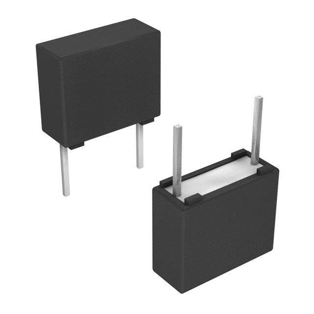
| 产品图片 |
|
| rohs | 符合RoHS无铅 / 符合限制有害物质指令(RoHS)规范要求 |
| 产品系列 | 时钟和计时器IC,时钟缓冲器,Silicon Labs Si5330G-B00218-GM- |
| 数据手册 | |
| 产品型号 | SI5330G-B00218-GMSi5330G-B00218-GM |
| 产品种类 | 时钟缓冲器 |
| 传播延迟—最大值 | 4 ns |
| 供应商器件封装 | 24-QFN(4x4) |
| 包装 | 管件 |
| 商标 | Silicon Labs |
| 安装类型 | 表面贴装 |
| 安装风格 | SMD/SMT |
| 封装 | Tray |
| 封装/外壳 | 24-VFQFN 裸露焊盘 |
| 封装/箱体 | QFN-24 |
| 工作温度 | -40°C ~ 85°C |
| 工厂包装数量 | 75 |
| 差分-输入:输出 | 是/无 |
| 最大工作温度 | + 85 C |
| 最大输入频率 | 200 MHz |
| 最大输出频率 | 200 MHz |
| 最小工作温度 | - 40 C |
| 标准包装 | 75 |
| 比率-输入:输出 | 1:8 |
| 电压-电源 | 1.71 V ~ 3.63 V |
| 电源电压-最大 | 3.63 V |
| 电源电压-最小 | 1.71 V |
| 电源电流 | 10 mA |
| 电路数 | 1 |
| 类型 | 扇出缓冲器(分配),变换器 |
| 系列 | SI5330G |
| 输入 | CML, HCSL, LVDS, LVPECL |
| 输入类型 | LVDS, LVPECL |
| 输出 | CMOS |
| 输出端数量 | 8 |
| 输出类型 | LVDS, LVPECL |
| 频率-最大值 | 200MHz |


- 商务部:美国ITC正式对集成电路等产品启动337调查
- 曝三星4nm工艺存在良率问题 高通将骁龙8 Gen1或转产台积电
- 太阳诱电将投资9.5亿元在常州建新厂生产MLCC 预计2023年完工
- 英特尔发布欧洲新工厂建设计划 深化IDM 2.0 战略
- 台积电先进制程称霸业界 有大客户加持明年业绩稳了
- 达到5530亿美元!SIA预计今年全球半导体销售额将创下新高
- 英特尔拟将自动驾驶子公司Mobileye上市 估值或超500亿美元
- 三星加码芯片和SET,合并消费电子和移动部门,撤换高东真等 CEO
- 三星电子宣布重大人事变动 还合并消费电子和移动部门
- 海关总署:前11个月进口集成电路产品价值2.52万亿元 增长14.8%


PDF Datasheet 数据手册内容提取
Si5330 1.8/2.5/3.3 V LOW-JITTER, LOW-SKEW CLOCK BUFFER/LEVEL TRANSLATOR Features Supports single-ended or Output-output skew: 100 ps differential input clock signals Propagation delay: 2.5 ns typ Generates four differential Single core supply with excellent (LVPECL, LVDS, HCSL) or eight PSRR: 1.8, 2.5, or 3.3 V single-ended (CMOS, SSTL, Output driver supply voltage HSTL) outputs independent of core supply: 1.5, Provides signal level translation 1.8, 2.5, or 3.3 V Differential to single-ended Loss of Signal (LOS) indicator Ordering Information: Single-ended to differential allows system clock monitoring Differential to differential Output Enable (OEB) pin allows See page 14. Single-ended to single-ended glitchless control of output clocks Wide frequency range Low power: 10 mA typical core Pin Assignments LVPECL, LVDS: 5 to 710 MHz current HCSL: 5 to 250 MHz Industrial temperature range: SSTL, HSTL: 5 to 350 MHz –40 to +85 °C CMOS: 5 to 200 MHz Small size: 24-lead, 4 x 4 mm Additive jitter: 150 fs RMS typ QFN Applications High Speed Clock Distribution PCI Express 2.0/3.0 Ethernet Switch/Router Fibre Channel SONET / SDH MSAN/DSLAM/PON Telecom Line Cards Functional Block Diagram Rev. 1.2 4/17 Copyright © 2017 by Silicon Laboratories Si5330
Si5330 * Functional Block Diagrams Based on Orderable Part Number Figure 1. Si5330 Functional Block Diagrams *Note: See Table 11 for detailed ordering information. 2 Rev. 1.2
Si5330 TABLE OF CONTENTS Section Page 1. Functional Block Diagrams Based on Orderable Part Number* . . . . . . . . . . . . . . . . . . .2 2. Electrical Specifications . . . . . . . . . . . . . . . . . . . . . . . . . . . . . . . . . . . . . . . . . . . . . . . . . . .4 3. Functional Description . . . . . . . . . . . . . . . . . . . . . . . . . . . . . . . . . . . . . . . . . . . . . . . . . . . .9 3.1. VDD and VDDO Supplies . . . . . . . . . . . . . . . . . . . . . . . . . . . . . . . . . . . . . . . . . . . . . .9 3.2. Loss Of Signal Indicator (LOS) . . . . . . . . . . . . . . . . . . . . . . . . . . . . . . . . . . . . . . . . . .9 3.3. Output Enable (OEB) . . . . . . . . . . . . . . . . . . . . . . . . . . . . . . . . . . . . . . . . . . . . . . . . .9 3.4. Input Signals . . . . . . . . . . . . . . . . . . . . . . . . . . . . . . . . . . . . . . . . . . . . . . . . . . . . . . . .9 3.5. Output Driver Formats . . . . . . . . . . . . . . . . . . . . . . . . . . . . . . . . . . . . . . . . . . . . . . . . .9 3.6. Input and Output Terminations . . . . . . . . . . . . . . . . . . . . . . . . . . . . . . . . . . . . . . . . . .9 4. Ordering the Si5330 . . . . . . . . . . . . . . . . . . . . . . . . . . . . . . . . . . . . . . . . . . . . . . . . . . . . . . .9 5. Pin Descriptions . . . . . . . . . . . . . . . . . . . . . . . . . . . . . . . . . . . . . . . . . . . . . . . . . . . . . . . . .10 6. Orderable Part Numbers and Device Functionality . . . . . . . . . . . . . . . . . . . . . . . . . . . .14 7. Package Outline: 24-Lead QFN . . . . . . . . . . . . . . . . . . . . . . . . . . . . . . . . . . . . . . . . . . . . .16 8. Recommended PCB Layout . . . . . . . . . . . . . . . . . . . . . . . . . . . . . . . . . . . . . . . . . . . . . . .17 9. Top Marking . . . . . . . . . . . . . . . . . . . . . . . . . . . . . . . . . . . . . . . . . . . . . . . . . . . . . . . . . . . .18 9.1. Si5330 Top Marking . . . . . . . . . . . . . . . . . . . . . . . . . . . . . . . . . . . . . . . . . . . . . . . . .18 9.2. Top Marking Explanation . . . . . . . . . . . . . . . . . . . . . . . . . . . . . . . . . . . . . . . . . . . . .18 Document Change List . . . . . . . . . . . . . . . . . . . . . . . . . . . . . . . . . . . . . . . . . . . . . . . . . . . . .19 Contact Information . . . . . . . . . . . . . . . . . . . . . . . . . . . . . . . . . . . . . . . . . . . . . . . . . . . . . . . .20 Rev. 1.2 3
Si5330 1. Electrical Specifications Table 1. Recommended Operating Conditions (V = 1.8 V –5% to +10%, 2.5 V ±10%, or 3.3 V ±10%, T = –40 to 85°C) DD A Parameter Symbol Test Condition Min Typ Max Unit Ambient Temperature T –40 25 85 °C A 2.97 3.3 3.63 V Core Supply Voltage V 2.25 2.5 2.75 V DD 1.71 1.8 1.98 V Output Buffer Supply V DDOn 1.4 — 3.63 V Voltage Note: All minimum and maximum specifications are guaranteed and apply across the recommended operating conditions. Typical values apply at nominal supply voltages and an operating temperature of 25 °C unless otherwise noted. Table 2. DC Characteristics (V = 1.8 V –5% to +10%, 2.5 V ±10%, or 3.3 V ±10%, T = –40 to 85°C) DD A Parameter Symbol Test Condition Min Typ Max Unit Core Supply Current I 50 MHz refclk — 10 — mA DD LVPECL, 710 MHz — — 30 mA LVDS, 710 MHz — — 8 mA HCSL, 250 MHz — — 20 mA 2 pF load capacitance SSTL, 350 MHz — — 19 mA Output Buffer Supply Current I DDOx CMOS, 50 MHz — — 28 mA 15 pF load capacitance CMOS, 200 MHz — — 28 mA 2 pF load capacitance HSTL, 350 MHz — — 19 mA 4 Rev. 1.2
Si5330 Table 3. Performance Characteristics (V = 1.8 V –5% to +10%, 2.5 V ±10%, or 3.3 V ±10%, T = –40 to 85°C) DD A Parameter Symbol Test Condition Min Typ Max Unit CLKIN Loss of Signal Assert t — 2.6 5 μs Time LOS CLKIN Loss of Signal De-Assert After initial start-up time has t 0.01 0.2 1 μs Time LOS_B expired Input-to-Output Propagation t — 2.5 4.0 ns Delay PROP Outputs at same signal Output-Output Skew t — — 100 ps DSKEW format Start-up time for output POR to Output Clock Valid t — — 2 ms START clocks Table 4. Input and Output Clock Characteristics (V = 1.8 V –5% to +10%, 2.5 V ±10%, or 3.3 V ±10%, T = –40 to 85 °C) DD A Parameter Symbol Test Condition Min Typ Max Units Input Clock (AC Coupled Differential Input Clocks on Pin IN1/2) Frequency fIN 5 — 710 MHz Differential Voltage Swing VPP 710 MHz input 0.4 — 2.4 VPP Rise/Fall Time tR/tF 20%–80% — — 1.0 ns Duty Cycle DC < 1 ns tr/tf 40 50 60 % Input Impedance RIN 10 — — k Input Capacitance CIN — 3.5 — pF Input Clock (DC-Coupled Single-Ended Input Clock on Pin IN3) CMOS 5 — 200 MHz Frequency fIN HSTL, SSTL 5 — 350 MHz Input Voltage VI –0.1 — VDD V Input Voltage Swing 200 MHz, Tr/Tf = 1.3 ns 0.8 — — Vpp (CMOS Standard) Rise/Fall Time tR/tF 20%–80% — — 4 ns Duty Cycle DC < 2 ns tr/tf 40 50 60 % Input Capacitance CIN — 2 — pF Output Clocks (Differential) LVPECL, LVDS 5 — 710 MHz Frequency fOUT HCSL 5 — 250 MHz Rev. 1.2 5
Si5330 Table 4. Input and Output Clock Characteristics (Continued) (V = 1.8 V –5% to +10%, 2.5 V ±10%, or 3.3 V ±10%, T = –40 to 85 °C) DD A Parameter Symbol Test Condition Min Typ Max Units V – V common mode — DDO — V OC 1.45 V LVPECL Output Voltage peak-to-peak single- V 0.55 0.8 0.96 V SEPP ended swing PP V common mode 1.125 1.2 1.275 V OC LVDS Output Voltage peak-to-peak single- (2.5/3.3 V) V 0.25 0.35 0.45 V SEPP ended swing PP V common mode 0.8 0.875 0.95 V OC LVDS Output Voltage peak-to-peak single- (1.8 V) V 0.25 0.35 0.45 V SEPP ended swing PP V common mode 0.35 0.375 0.400 V OC HCSL Output Voltage peak-to-peak single- V 0.575 0.725 0.85 V SEPP ended swing PP Rise/Fall Time tR/tF 20%–80% — — 450 ps CKn < 350 MHz 45 — 55 % Duty Cycle* DC 350 MHz < CLKn < 40 — 60 % 710 MHz Output Clocks (Single-Ended) CMOS 5 — 200 MHz Frequency fOUT SSTL, HSTL 5 — 350 MHz CMOS 20%-80% t /t 2 pF load — 0.45 0.85 ns Rise/Fall Time R F CMOS 20%-80% t /t 15 pF load — — 2.0 ns Rise/Fall Time R F CMOS Output — 50 — Resistance SSTL Output Resistance — 50 — HSTL Output Resistance — 50 — V 4 mA load VDDO–0.3 — V OH CMOS Output Voltage V 4 mA load — 0.3 V OL V 0.45xVDDO+0.41 — — V OH SSTL-3 VDDOx = 2.97 to V 3.63 V — — 0.45xVDDO V OL –0.41 V 0.5xVDDO+0.41 — — V OH SSTL-2 VDDOx = 2.25 to SSTL Output Voltage V 2.75 V — — 0.5xVDDO– V OL 0.41 V 0.5xVDDO+0.34 — V OH SSTL-18 VDDOx = 1.71 V to 1.98 V — — 0.5xVDDO– V OL 0.34 6 Rev. 1.2
Si5330 Table 4. Input and Output Clock Characteristics (Continued) (V = 1.8 V –5% to +10%, 2.5 V ±10%, or 3.3 V ±10%, T = –40 to 85 °C) DD A Parameter Symbol Test Condition Min Typ Max Units V 0.5xVDDO +0.3 — — V OH HSTL Output Voltage VDDO = 1.4 to 1.6 V 0.5xVDDO V — — V OL –0.3 Duty Cycle* DC 45 — 55 % *Note: Input clock has a 50% duty cycle. Table 5. OEB Input Specifications Parameter Symbol Test Condition Min Typ Max Unit Input Voltage Low V — — 0.3 x V V IL DD Input Voltage High V 0.7 x V — — V IH DD Input Resistance R 20 — — k IN Table 6. Output Control Pins (LOS) (V = 1.8 V –5% to +10%, 2.5 V ±10%, or 3.3 V ±10%, T = –40 to 85 °C) DD A Parameter Symbol Condition Min Typ Max Unit Output Voltage Low V I = 3 mA 0 — 0.4 V OL SINK Rise/Fall Time 20–80% t /t C < 10 pf, pull up 1 k — — 10 ns R F L Table 7. Jitter Specifications (V = 1.8 V –5% to +10%, 2.5 V ±10%, or 3.3 V ±10%, T = –40 to 85°C) DD A Parameter Symbol Test Condition Min Typ Max Unit 0.7 V pk-pk differential input Additive Phase Jitter t clock at 622.08 MHz with — 0.150 — ps RMS RPHASE (12 kHz–20 MHz) 70 ps rise/fall time 0.7 V pk-pk differential input Additive Phase Jitter t clock at 622.08 MHz with — 0.225 — ps RMS RPHASEWB (50 kHz–80 MHz) 70 ps rise/fall time Table 8. Thermal Characteristics Parameter Symbol Test Condition Value Unit Thermal Resistance Still Air 37 °C/W Junction to Ambient JA Thermal Resistance Still Air 25 °C/W Junction to Case JC Rev. 1.2 7
Si5330 Table 9. Absolute Maximum Ratings1,2,3,4 Parameter Symbol Test Condition Value Unit DC Supply Voltage V –0.5 to 3.8 V DD Storage Temperature Range T –55 to 150 °C STG HBM ESD Tolerance 2.5 kV (100 pF, 1.5 k) ESD Tolerance CDM 550 V ESD Tolerance MM 175 V Latch-up Tolerance JESD78 Compliant Junction Temperature T 150 °C J Soldering Temperature T 260 °C PEAK (Pb-free profile)4 Soldering Temperature Time at T T 20–40 sec PEAK P (Pb-free profile)4 Notes: 1. Permanent device damage may occur if the Absolute Maximum Ratings are exceeded. Functional operation should be restricted to the conditions as specified in the operational sections of this data sheet. Exposure to maximum rating conditions for extended periods may affect device reliability. 2. 24-QFN package is RoHS compliant. 3. For more packaging information, go to www.silabs.c om/support/quality/pages/RoHSInformation.aspx. 4. Recommended card reflow profile is per the JEDEC/IPC J-STD-020 specification for Small Body Components. 8 Rev. 1.2
Si5330 2. Functional Description 2.3. Output Enable (OEB) The output enable (OEB) pin allows disabling or The Si5330 is a low-jitter, low-skew fanout buffer enabling of the outputs clocks (CLK0-CLK3). The output optimized for high-performance PCB clock distribution enable is logically controlled to ensure that no glitches applications. The device produces four differential or or runt pulses are generated at the output as shown in eight single-ended, low-jitter output clocks from a single Figure 3. input clock. The input can accept either a single-ended or a differential clock allowing the device to function as a clock level translator. 2.1. V and V Supplies DD DDO The core V and output V supplies have separate DD DDO and independent supply pins allowing the core supply to operate at a different voltage than the I/O voltage levels. Figure 3. OEB Glitchless Operation The V supply powers the core functions of the device, DD All outputs are enabled when the OEB pin is connected which operates from 1.8, 2.5, or 3.3 V. Using a lower to ground or below the V voltage for this pin. IL supply voltage helps minimize the device’s power Connecting the OEB pin to VDD or above the V level IH consumption. The V supply pins are used to set the DDO will disable the outputs. Both V and V are specified IL IH output signal levels and must be set at a voltage level in Table 5. All outputs are forced to a logic “low” when compatible with the output signal format. disabled. The OEB pin is 3.3 V tolerant. 2.2. Loss Of Signal Indicator (LOS) 2.4. Input Signals The input is monitored for a valid clock signal using an The Si5330 can accept single-ended and differential LOS circuit that monitors input clock edges and input clocks. See “AN408: Termination Options for Any- declares an LOS condition when signal edges are n ot Frequency, Any-Output Clock Generators and Clock detected over a 1 to 5 μs observation period. The LOS Buffers—Si5338, Si5334, Si5330” for details on pin is asserted “low” when activity on the input clock pin connecting a wide variety of signals to the Si5330 is present. A “high” level on the LOS pin indicates a loss inputs. of signal (LOS). The LOS pin must be pulled to VDD as 2.5. Output Driver Formats shown in Figure 2. The Si5330 supports single-ended output formats of CMOS, SSTL, and HSTL and differential formats of LVDS, LVPECL, and HCSL. It is normally required that the LVDS driver be dc-coupled to the 100 termination at the receiver end. If your application requires an ac- coupled 100 load, contact the applications team for advice. See AN408 for additional information on the terminations for these driver types. 2.6. Input and Output Terminations See AN408 for detailed information. 3. Ordering the Si5330 The Si5330 can be ordered to meet the requirements of the most commonly-used input and output signal types, such as CMOS, SSTL, HSTL, LVPECL, LVDS, and HSCL. See Figure 1, “Si5330 Functional Block Figure 2. LOS Indicator with External Pull-Up Diagrams,” on page 2 and Table 11, “Order Numbers and Device Functionality,” on page 14 for specific ordering information. Rev. 1.2 9
Si5330 4. Pin Descriptions Note: Center pad must be tied to GND for normal operation. Table 10. Si5330 Pin Descriptions Pin # Pin Name I/O Signal Type Description 1 IN1 I Multi Si5330A/B/C/G/H/J Differential Input Devices. IN2 I Multi These pins are used as the differential clock input. IN1 is the positive input; IN2 is the negative input. Refer to “AN408: Termination Options for Any-Frequency, Any- Output Clock Generators and Clock Buffers—Si5338, 2 Si5334, Si5330” for interfacing and termination details. Si5330F/K/L/M Single-Ended Input Devices. These pins are not used. Leave IN1 unconnected and IN2 connected to ground. Si5330F/K/L/M Single-Ended Devices. This is the single-ended clock input. Refer to AN408 for 3 IN3 I Multi interfacing and termination details. Si5330A/B/C/G/H/J Differential Input Devices. This pin is not used. Connect to ground. Ground. 4 RSVD_GND Must be connected to system ground. Ground. 5 RSVD_GND Must be connected to system ground. Ground. 6 RSVD_GND Must be connected to system ground. 10 Rev. 1.2
Si5330 Table 10. Si5330 Pin Descriptions (Continued) Pin # Pin Name I/O Signal Type Description Core Supply Voltage. The device operates from a 1.8, 2.5, or 3.3 V supply. A 7 VDD VDD Supply 0.1 μF bypass capacitor should be located very close to this pin. Loss of Signal Indicator. 0 = CLKIN present. 8 LOS O Open Drain 1 = Loss of signal (LOS). This pin requires an external 1kpull-up resistor. Si5330A/B/C/K/L/M Differential Output Devices. This is the negative side of the differential CLK3 output. Refer to AN408 for interfacing and termination details. Leave unconnected when not in use. 9 CLK3B O Multi Si5330F/G/H/J Single-Ended Output Devices. This is one of the single-ended CLK3 outputs. Both CLK3A and CLK3B single-ended outputs are in phase. Refer to AN408 for interfacing and termination details. Leave unconnected when not is use. Si5330A/B/C/K/L/M Differential Devices. This is the positive side of the differential CLK3 output. Refer to AN408 for interfacing and termination details. Leave unconnected when not in use. 10 CLK3A O Multi Si5330F/G/H/J Single-Ended Devices. This is one of the single-ended CLK3 outputs. Both CLK3A and CLK3B single-ended outputs are in phase. Refer to AN408 for interfacing and termination details. Leave unconnected when not is use. Output Clock Supply Voltage. Supply voltage for CLK3A/B. Use a 0.1 μF bypass cap 11 VDDO3 VDD Supply as close as possible to this pin. If CLK3 is not used, this pin must be tied to V (pin 7 and/or pin 24). DD Ground. 12 RSVD_GND Must be connected to system ground. Si5330A/B/C/K/L/M Differential Output Devices. This is the negative side of the differential CLK2 output. Refer to AN408 for interfacing and termination details. Leave unconnected when not in use. 13 CLK2B O Multi Si5330F/G/H/J Single-Ended Output Devices. This is one of the single-ended CLK2 outputs. Both CLK2A and CLK2B single-ended outputs are in phase. Refer to AN408 for interfacing and termination details. Leave unconnected when not is use. Rev. 1.2 11
Si5330 Table 10. Si5330 Pin Descriptions (Continued) Pin # Pin Name I/O Signal Type Description Si5330A/B/C/K/L/M Differential Devices. This is the positive side of the differential CLK2 output. Refer to AN408 for interfacing and termination details. Leave unconnected when not in use. 14 CLK2A O Multi Si5330F/G/H/J Single-Ended Devices. This is one of the single-ended CLK2 outputs. Both CLK2A and CLK2B single-ended outputs are in phase. Refer to AN408 for interfacing and termination details. Leave unconnected when not is use. Output Clock Supply Voltage. Supply voltage for CLK2A/B. Use a 0.1 μF bypass cap 15 VDDO2 VDD Supply as close as possible to this pin. If CLK2 is not used, this pin must be tied to V (pin 7 and/or pin 24). DD Output Clock Supply Voltage. Supply voltage for CLK1A,B. Use a 0.1 μF bypass cap 16 VDDO1 VDD Supply as close as possible to this pin. If CLK1 is not used, this pin must be tied to V (pin 7 and/or pin 24). DD Si5330A/B/C/K/L/M Differential Output Devices. This is the negative side of the differential CLK1 output. Refer to AN408 for interfacing and termination details. Leave unconnected when not in use. 17 CLK1B O Multi Si5330F/G/H/J Single-Ended Output Devices. This is one of the single-ended CLK1 outputs. Both CLK1A and CLK1B single-ended outputs are in phase. Refer to AN408 for interfacing and termination details. Leave unconnected when not is use. Si5330A/B/C/K/L/M Differential Devices. This is the positive side of the differential CLK1 output. Refer to AN408 for interfacing and termination details. Leave unconnected when not in use. 18 CLK1A O Multi Si5330F/G/H/J Single-Ended Devices. This is one of the single-ended CLK1 outputs. Both CLK1A and CLK1B single-ended outputs are in phase. Refer to AN408 for interfacing and termination details. Leave unconnected when not is use. Output Enable. All outputs are enabled when the OEB pin is connected to ground or below the V voltage for this pin. Connect- IL 19 OEB I CMOS ing the OEB pin to V or above the V level will dis- DD IH able the outputs. Both V and V are specified in IL IH Table 5. All outputs are forced to a logic “low” when dis- abled. This pin is 3.3 V tolerant. Output Clock Supply Voltage. Supply voltage for CLK0A,B. Use a 0.1 μF bypass cap 20 VDDO0 VDD Supply as close as possible to this pin. If CLK2 is not used, this pin must be tied to V (pin 7 and/or pin 24). DD 12 Rev. 1.2
Si5330 Table 10. Si5330 Pin Descriptions (Continued) Pin # Pin Name I/O Signal Type Description Si5330A/B/C/K/L/M Differential Output Devices. This is the negative side of the differential CLK0 output. Refer to AN408 for interfacing and termination details. Leave unconnected when not in use. 21 CLK0B O Multi Si5330F/G/H/J Single-ended Output Devices. This is one of the single-ended CLK0 outputs. Both CLK0A and CLK0B single-ended outputs are in phase. Refer to AN408 for interfacing and termination details. Leave unconnected when not is use. Si5330A/B/C/K/L/M Differential Devices. This is the positive side of the differential CLK0 output. Refer to AN408 for interfacing and termination details. Leave unconnected when not in use. 22 CLK0A O Multi Si5330F/G/H/J Single-ended Devices. This is one of the single-ended CLK0 outputs. Both CLK0A and CLK0B single-ended outputs are in phase. Refer to AN408 for interfacing and termination details. Leave unconnected when not is use. Ground. 23 RSVD_GND Must be connected to system ground. Core Supply Voltage. The device operates from a 1.8, 2.5, or 3.3 V supply. A 24 VDD VDD Supply 0.1 μF bypass capacitor should be located very close to this pin. Ground Pad. This is main ground connection for this device. It is GND located at the bottom center of the package. Use as GND GND Supply PAD many vias as possible to connect this pad to the main ground plane. The device will not function as specified unless this ground pad is properly connected to ground. Rev. 1.2 13
Si5330 5. Orderable Part Numbers and Device Functionality Table 11. Order Numbers and Device Functionality Part Number1,2 Input Signal Output Signal Number Frequency Format Format of Range Outputs LVPECL Buffers Si5330A-B00200-GM Differential 3.3 V LVPECL 4 5 to 710 MHz Si5330A-B00202-GM Differential 2.5 V LVPECL 4 5 to 710 MHz LVDS Buffers Si5330B-B00204-GM Differential 3.3 V LVDS 4 5 to 710 MHz Si5330B-B00205-GM Differential 2.5 V LVDS 4 5 to 710 MHz Si5330B-B00206-GM Differential 1.8 V LVDS 4 5 to 710 MHz HCSL Buffers Si5330C-B00207-GM Differential 3.3 V HCSL 4 5 to 250 MHz Si5330C-B00208-GM Differential 2.5 V HCSL 4 5 to 250 MHz Si5330C-B00209-GM Differential 1.8 V HCSL 4 5 to 250 MHz CMOS Buffers Si5330F-B00214-GM Single-Ended 3.3 V CMOS 8 5 to 200 MHz Si5330F-B00215-GM Single-Ended 2.5 V CMOS 8 5 to 200 MHz Si5330F-B00216-GM Single-Ended 1.8 V CMOS 8 5 to 200 MHz CMOS Buffers (Differential Input) Si5330G-B00217-GM Differential 3.3 V CMOS 8 5 to 200 MHz Si5330G-B00218-GM Differential 2.5 V CMOS 8 5 to 200 MHz Si5330G-B00219-GM Differential 1.8 V CMOS 8 5 to 200 MHz SSTL Buffers (Differential Input) Si5330H-B00220-GM Differential 3.3 V SSTL 8 5 to 350 MHz Si5330H-B00221-GM Differential 2.5 V SSTL 8 5 to 350 MHz Si5330H-B00222-GM Differential 1.8 V SSTL 8 5 to 350 MHz HSTL Buffers (Differential Input) Si5330J-B00223-GM Differential 1.5 V HSTL 8 5 to 350 MHz LVPECL Buffers (Single-Ended Input) Si5330K-B00224-GM Single-Ended 3.3 V LVPECL 4 5 to 350 MHz Si5330K-B00226-GM Single-Ended 2.5 V LVPECL 4 5 to 350 MHz Notes: 1. Custom configurations with mixed output types are also available. Please contact the factory for ordering details. 2. Add an “R” to the part number to specify tape and reel shipment media. When specifying non-tape-and-reel shipment media, contact your sales representative for more information. 14 Rev. 1.2
Si5330 Table 11. Order Numbers and Device Functionality (Continued) Part Number1,2 Input Signal Output Signal Number Frequency Format Format of Range Outputs LVDS Buffers (Single-Ended Input) Si5330L-B00228-GM Single-Ended 3.3 V LVDS 4 5 to 350 MHz Si5330L-B00229-GM Single-Ended 2.5 V LVDS 4 5 to 350 MHz Si5330L-B00230-GM Single-Ended 1.8 V LVDS 4 5 to 350 MHz HCSL Buffers (Single-Ended Input) Si5330M-B00231-GM Single-Ended 3.3 V HCSL 4 5 to 250 MHz Si5330M-B00232-GM Single-Ended 2.5 V HCSL 4 5 to 250 MHz Si5330M-B00233-GM Single-Ended 1.8 V HCSL 4 5 to 250 MHz Notes: 1. Custom configurations with mixed output types are also available. Please contact the factory for ordering details. 2. Add an “R” to the part number to specify tape and reel shipment media. When specifying non-tape-and-reel shipment media, contact your sales representative for more information. Rev. 1.2 15
Si5330 6. Package Outline: 24-Lead QFN Figure 4. 24-Lead Quad Flat No-Lead (QFN) Table 12. Package Dimensions Dimension Min Nom Max A 0.80 0.85 0.90 A1 0.00 0.02 0.05 b 0.18 0.25 0.30 D 4.00 BSC. D2 2.35 2.50 2.65 e 0.50 BSC. E 4.00 BSC. E2 2.35 2.50 2.65 L 0.30 0.40 0.50 aaa 0.10 bbb 0.10 ccc 0.08 ddd 0.10 eee 0.05 Notes: 1. All dimensions shown are in millimeters (mm) unless otherwise noted. 2. Dimensioning and Tolerancing per ANSI Y14.5M-1994. 3. This drawing conforms to the JEDEC Outline MO-220, variation VGGD-8. 4. Recommended card reflow profile is per the JEDEC/IPC J-STD-020 specification for Small Body Components. 5. Terminal base alloy: Cu. 6. Terminal plating/grid array material: Au/NiPd. 7. For more packaging information, go to www.silabs.com/support/quality/pages/RoHSInformation.aspx. 16 Rev. 1.2
Si5330 7. Recommended PCB Layout Table 13. PCB Land Pattern Dimension Min Nom Max P1 2.50 2.55 2.60 P2 2.50 2.55 2.60 X1 0.20 0.25 0.30 Y1 0.75 0.80 0.85 C1 3.90 C2 3.90 E 0.50 Notes: General 1. All dimensions shown are in millimeters (mm) unless otherwise noted. 2. Dimensioning and Tolerancing per ANSI Y14.5M-1994 specification. 3. This Land Pattern Design is based on the IPC-7351 guidelines. 4. Connect the center ground pad to a ground plane with no less than five vias to a ground plane that is no more than 20 mils below it. Via drill size should be no smaller than 10 mils. A longer distance to the ground plane is allowed if more vias are used to keep the inductance from increasing. Solder Mask Design 5. All metal pads are to be non-solder mask defined (NSMD). Clearance between the solder mask and the metal pad is to be 60 μm minimum, all the way around the pad. Stencil Design 6. A stainless steel, laser-cut and electro-polished stencil with trapezoidal walls should be used to assure good solder paste release. 7. The stencil thickness should be 0.125 mm (5 mils). 8. The ratio of stencil aperture to land pad size should be 1:1 for all perimeter pins. 9. A 2x2 array of 1.0 mm square openings on 1.25 mm pitch should be used for the center ground pad. Card Assembly 10. A No-Clean, Type-3 solder paste is recommended. 11. The recommended card reflow profile is per the JEDEC/IPC J-STD-020C specification for Small Body Components. Rev. 1.2 17
Si5330 8. Top Marking 8.1. Si5330 Top Marking 8.2. Top Marking Explanation Mark Method: Laser Line 1 Marking: Device Part Number Si5330 Line 2 Marking: X = Frequency and configuration code. Xxxxxx xxxxx = Input and output format configu- ration code. See "5. Orderable Part Numbers and Device Functionality" on page 14 for more information. Line 3 Marking: R = Product revision. RTTTTT TTTTT = Manufacturing trace code. Line 4 Marking: Pin 1 indicator. Circle with 0.5 mm diameter; left-justified YY = Year. YYWW WW = Work week. Characters correspond to the year and work week of package assembly. 18 Rev. 1.2
Si5330 DOCUMENT CHANGE LIST Revision 0.1 to Revision 0.2 Clarified documentation to reflect that Pin 19 is OEB (OE Enable Low). Updated Table 4, “Jitter Specifications” on page 7. Revision 0.2 to Revision 0.3 Major editorial updates to improve clarity. Updated “Additive Jitter” Specification Table. Updated “Core Supply Current” Specification in Table 2. Removed the Low-Power LVPECL output options from the ordering table in section 5. Removed D/E ordering options. Revision 0.3 to Revision 0.35 Typo of 150 ps on front page changed to 150 fs. Updated PCB layout notes. Added no ac coupling for LVDS outputs. Changed input rise/fall time spec to 2 ns. Revision 0.35 to Revision 1.0 Added maximum junction temperature specification to Table 9 on page 8. Added minimum and maximum duty cycle specifications to Table 4 on page 5. Updated Table 3, “Performance Characteristics,” on page 5. Added maximum propagation delay spec (4 ns). Added test condition to tLOS_B in Table 3 on page 5. Removed reference to frequency in Output-Output Skew. Updated Table 4, “Input and Output Clock Characteristics,” on page 5. Input voltage (max) changed “3.63” to “VDD” Input voltage swing (max) change “3.63” with “—”. Added Table 6, “Output Control Pins (LOS),” on page 7. Added tape and reel ordering information to "5. Orderable Part Numbers and Device Functionality" on page 14. Added "8. Top Marking" on page 18. Revision 1.0 to Revision 1.1 Updated ordering information to refer to revision B silicon. Updated top marking explanation in section 8.2. Revision 1.1 to Revision 1.2 Removed MSL rating. Rev. 1.2 19
ClockBuilder Pro One-click access to Timing tools, documentation, software, source code libraries & more. Available for Windows and iOS (CBGo only). www.silabs.com/CBPro Timing Portfolio SW/HW Quality Support and Community www.silabs.com/timing www.silabs.com/CBPro www.silabs.com/quality community.silabs.com Disclaimer Silicon Labs intends to provide customers with the latest, accurate, and in-depth documentation of all peripherals and modules available for system and software implementers using or intending to use the Silicon Labs products. Characterization data, available modules and peripherals, memory sizes and memory addresses refer to each specific device, and "Typical" parameters provided can and do vary in different applications. Application examples described herein are for illustrative purposes only. Silicon Labs reserves the right to make changes without further notice and limitation to product information, specifications, and descriptions herein, and does not give warranties as to the accuracy or completeness of the included information. Silicon Labs shall have no liability for the consequences of use of the information supplied herein. This document does not imply or express copyright licenses granted hereunder to design or fabricate any integrated circuits. The products are not designed or authorized to be used within any Life Support System without the specific written consent of Silicon Labs. A "Life Support System" is any product or system intended to support or sustain life and/or health, which, if it fails, can be reasonably expected to result in significant personal injury or death. Silicon Labs products are not designed or authorized for military applications. Silicon Labs products shall under no circumstances be used in weapons of mass destruction including (but not limited to) nuclear, biological or chemical weapons, or missiles capable of delivering such weapons. Trademark Information Silicon Laboratories Inc.® , Silicon Laboratories®, Silicon Labs®, SiLabs® and the Silicon Labs logo®, Bluegiga®, Bluegiga Logo®, Clockbuilder®, CMEMS®, DSPLL®, EFM®, EFM32®, EFR, Ember®, Energy Micro, Energy Micro logo and combinations thereof, "the world’s most energy friendly microcontrollers", Ember®, EZLink®, EZRadio®, EZRadioPRO®, Gecko®, ISOmodem®, Precision32®, ProSLIC®, Simplicity Studio®, SiPHY®, Telegesis, the Telegesis Logo®, USBXpress® and others are trademarks or registered trademarks of Silicon Labs. ARM, CORTEX, Cortex-M3 and THUMB are trademarks or registered trademarks of ARM Holdings. Keil is a registered trademark of ARM Limited. All other products or brand names mentioned herein are trademarks of their respective holders. Silicon Laboratories Inc. 400 West Cesar Chavez Austin, TX 78701 USA http://www.silabs.com