ICGOO在线商城 > 集成电路(IC) > PMIC - 以太网供电(PoE) 控制器 > Si3402-A-GM
- 型号: Si3402-A-GM
- 制造商: Silicon Laboratories
- 库位|库存: xxxx|xxxx
- 要求:
| 数量阶梯 | 香港交货 | 国内含税 |
| +xxxx | $xxxx | ¥xxxx |
查看当月历史价格
查看今年历史价格
Si3402-A-GM产品简介:
ICGOO电子元器件商城为您提供Si3402-A-GM由Silicon Laboratories设计生产,在icgoo商城现货销售,并且可以通过原厂、代理商等渠道进行代购。 Si3402-A-GM价格参考。Silicon LaboratoriesSi3402-A-GM封装/规格:PMIC - 以太网供电(PoE) 控制器, Power Over Ethernet Controller 1 Channel 802.3af (PoE) 20-QFN (5x5)。您可以下载Si3402-A-GM参考资料、Datasheet数据手册功能说明书,资料中有Si3402-A-GM 详细功能的应用电路图电压和使用方法及教程。
| 参数 | 数值 |
| 产品目录 | 集成电路 (IC)半导体 |
| 描述 | IC POE PD LOW EMI SW REG 20VQFN热交换电压控制器 PoE Powered Device up to 17W, low-EM |
| 产品分类 | PMIC - 以太网供电 (PoE) 控制器集成电路 - IC |
| 品牌 | Silicon LabsSilicon Laboratories Inc |
| 产品手册 | |
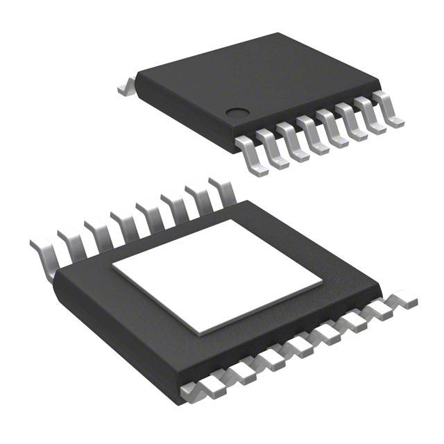
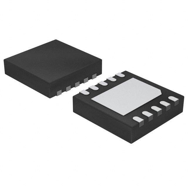
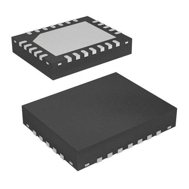
| 产品图片 |
|
| rohs | 符合RoHS无铅 / 符合限制有害物质指令(RoHS)规范要求 |
| 产品系列 | 电源管理 IC,热交换电压控制器,Silicon Labs Si3402-A-GM- |
| 数据手册 | |
| 产品型号 | SI3402-A-GMSi3402-A-GM |
| 产品 | PoE / LAN Solutions |
| 产品种类 | 热交换电压控制器 |
| 供应商器件封装 | 20-QFN(5x5) |
| 内部开关 | 是 |
| 功率-最大值 | 15W |
| 功率耗散 | 1.2 W |
| 包装 | 管件 |
| 单位重量 | 61.590 mg |
| 商标 | Silicon Labs |
| 安装风格 | SMD/SMT |
| 封装 | Tray |
| 封装/外壳 | 20-VQFN 裸露焊盘 |
| 封装/箱体 | QFN-20 |
| 工作温度 | -40°C ~ 85°C |
| 工作温度范围 | - 40 C to + 85 C |
| 工厂包装数量 | 60 |
| 标准 | 802.3af (PoE) |
| 标准包装 | 60 |
| 电压-电源 | 2.8 V ~ 57 V |
| 电流-电源 | 2mA |
| 电流限制 | 680 mA |
| 电源电压-最大 | 57 V |
| 电源电压-最小 | 2.8 V |
| 电源电流 | 2 mA |
| 类型 | 控制器 (PD) |
| 系列 | Si3402 |
| 辅助作用 | 无 |
| 输入/电源电压—最大值 | 57 V |
| 输入/电源电压—最小值 | 2.8 V |
| 通道数 | 1 |
| 配用 | /product-detail/zh/SI3402-EVB/336-1827-ND/2174845/product-detail/zh/SI3402ISO-EVB/336-1828-ND/2174836 |


- 商务部:美国ITC正式对集成电路等产品启动337调查
- 曝三星4nm工艺存在良率问题 高通将骁龙8 Gen1或转产台积电
- 太阳诱电将投资9.5亿元在常州建新厂生产MLCC 预计2023年完工
- 英特尔发布欧洲新工厂建设计划 深化IDM 2.0 战略
- 台积电先进制程称霸业界 有大客户加持明年业绩稳了
- 达到5530亿美元!SIA预计今年全球半导体销售额将创下新高
- 英特尔拟将自动驾驶子公司Mobileye上市 估值或超500亿美元
- 三星加码芯片和SET,合并消费电子和移动部门,撤换高东真等 CEO
- 三星电子宣布重大人事变动 还合并消费电子和移动部门
- 海关总署:前11个月进口集成电路产品价值2.52万亿元 增长14.8%


PDF Datasheet 数据手册内容提取
Si3402-A-GM to Si3402-B-GM EVB Modifications Version 0.4 The Si3402-B-GM device requires component value changes from those used with the Si3402-A-GM evaluation board (EVB) reference design. Table 1 below is a summary of the required modifications. Following Table 1 are two reference schematic excerpts showing the locations of the modified component values for both the isolated (flyback) and non-isolated (buck) topologies. Table 1. Si3402-B-GM EVB modifications versus the Si3402-A-GM EVB Item Modification description Application design effect M1 Detect resistor value The former 25.5kΩ detect resistor must be replaced by 24.3kΩ change 1% M2 Classification resistor value The following 1% resistors must be used: change Class0: 681.00 or higher (It is optional to place this resistor) Class1: 140.0 Class2: 75.0 Class3: 48.7 Class4: 33.2 M3* ISO EVB DCDC 3.3V changes Flyback C8, R9 & C23 are not need—Do not populate them. C9=10nF, C21=33nF, R12=475 Ω & R8=1.1k Ω Replace D2 (DFLT15A) with DFLT30A * See Revision Notes M4 ISO EVB DCDC 5V changes Flyback C8, R9 & C23 are not need—Do not populate them. C9=3.3nF, C21=15nF, R12=0 & R8=0 (place zero Ω resistors) Replace D2 (DFLT15A) with DFLT30A M5 ISO EVB DCDC 12V changes Flyback C8, R9 & C23 are not need—Do not populate them. C9=10nF, C21=15nF, R12=0, R8=0 (place zero Ω resistor) R7=3k Replace D2 (DFLT15A) with DFLT30A M6 DCDC reference voltage change (Buck case only) Now 1.35V instead of previous 1.23V. Thus, R5 changes from 2.87kΩ 1% to 3.24kΩ 1%. R6 (1%) is modified according to this table: SILICON LABS CONFIDENTIAL
Vout Target R5 kΩ R6 kΩ Vref Vout Measured 3.3 3.24 4.64 1.35 3.37 5 3.24 8.66 1.35 4.96 9 3.24 18.2 1.35 8.93 12 3.24 25.5 1.35 11.98 M7 BUCK EVB DCDC 3.3V compensation network C19, C20 & C9 are not need—Do not populate them. changes R8 can be populated with a 0Ω resistor (creating a short between pins 3 and 4) or left unpopulated, since the ISOSSFT function is now internal (see datasheet). C7=1nF, R7=47kΩ ±20%. M8 BUCK EVB DCDC 5V compensation network C19, C20, R8 & C9 are not need—Do not populate them. changes R8 can be populated with a 0Ω resistor (creating a short between pins 3 and 4) or left unpopulated, since the ISOSSFT function is now internal (see datasheet). C7=1nF, R7=47kΩ ±20%. M9 BUCK EVB DCDC 12V compensation network C19, C20, R8 & C9 are not need—Do not populate them. changes R8 can be populated with a 0Ω resistor (creating a short between pins 3 and 4) or left unpopulated, since the ISOSSFT function is now internal (see datasheet). C7=1nF, R7=47kΩ ±20%. SILICON LABS CONFIDENTIAL
Si3402ISO (Flyback, Isolated) EVB Reference Design – 5V S e e M 2 2 4 .3 DFLT30A k Ω 0Ω 15nF 3 .3 n F 0 Ω SILICON LABS CONFIDENTIAL
Si3402 (Buck, Non-Isolated) EVB Reference Design - 5V S e e M 2 2 4 .3 k Ω 1 See nF See M M 7-M 47kΩ 6 9 SILICON LABS CONFIDENTIAL
Revision Notes 26 August 2015: Added B5 indicating the Si3402-B-EN1 samples should be run only at room temperature Clarified Buck (Non-Isolated) case R7 to standard value 47kΩ and relaxed to 20% tolerance 28 October 2015: Previous version silicon errata resolved Several components in the change list updated Document renamed “Si3402-B RevA3 Change List_<YYYYMMDD>” 24 November 2015: M2 and M6 components updated Aligns with production Si3402-B-GM silicon 08 December 2015: (Version 0.3) Changed title of doc and name of file Clarified M7-M9 changes with regard to R8 21 March 2016: (Version 0.4) Updated M3, the 3.3V Isolated Flyback case. o Explanation: 3.3V Flyback compensation was updated to address a small overshoot condition under no-load conditions (3.66V is allowed, the overshoot was 3.73V). The problem is fixed with revised compensation with a resulting overshoot of about 3.5V. o If a no-load condition is unlikely, the customer may keep the original M3 change recommendation: C8, R9 & C23 are not need—Do not populate them C9=3.3nF, C21=15nF, R12=0 & R8=0 (place zero Ω resistors) Replace D2 (DFLT15A) with DFLT30A SILICON LABS CONFIDENTIAL
 Datasheet下载