ICGOO在线商城 > 集成电路(IC) > 线性 - 放大器 - 仪表,运算放大器,缓冲器放大器 > SY88303BLEY
- 型号: SY88303BLEY
- 制造商: Micrel
- 库位|库存: xxxx|xxxx
- 要求:
| 数量阶梯 | 香港交货 | 国内含税 |
| +xxxx | $xxxx | ¥xxxx |
查看当月历史价格
查看今年历史价格
SY88303BLEY产品简介:
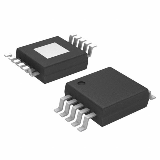
ICGOO电子元器件商城为您提供SY88303BLEY由Micrel设计生产,在icgoo商城现货销售,并且可以通过原厂、代理商等渠道进行代购。 SY88303BLEY价格参考。MicrelSY88303BLEY封装/规格:线性 - 放大器 - 仪表,运算放大器,缓冲器放大器, 限制 放大器 1 电路 差分 10-MSOP-EP。您可以下载SY88303BLEY参考资料、Datasheet数据手册功能说明书,资料中有SY88303BLEY 详细功能的应用电路图电压和使用方法及教程。
| 参数 | 数值 |
| -3db带宽 | 2GHz |
| 产品目录 | 集成电路 (IC) |
| 描述 | IC OPAMP LIMITING 2GHZ 10MSOP |
| 产品分类 | Linear - Amplifiers - Instrumentation, OP Amps, Buffer Amps |
| 品牌 | Micrel Inc |
| 数据手册 | |
| 产品图片 |
|
| 产品型号 | SY88303BLEY |
| rohs | 无铅 / 符合限制有害物质指令(RoHS)规范要求 |
| 产品系列 | - |
| 产品目录页面 | |
| 供应商器件封装 | 10-MSOP-EP |
| 其它名称 | 576-2988 |
| 包装 | 管件 |
| 压摆率 | - |
| 增益带宽积 | - |
| 安装类型 | 表面贴装 |
| 封装/外壳 | 10-TFSOP,10-MSOP(0.118",3.00mm 宽)裸焊盘 |
| 工作温度 | -40°C ~ 85°C |
| 放大器类型 | 限制 |
| 标准包装 | 100 |
| 电压-电源,单/双 (±) | 3 V ~ 3.6 V |
| 电压-输入失调 | - |
| 电流-电源 | 38mA |
| 电流-输入偏置 | - |
| 电流-输出/通道 | 50mA |
| 电路数 | 1 |
| 输出类型 | 差分 |


- 商务部:美国ITC正式对集成电路等产品启动337调查
- 曝三星4nm工艺存在良率问题 高通将骁龙8 Gen1或转产台积电
- 太阳诱电将投资9.5亿元在常州建新厂生产MLCC 预计2023年完工
- 英特尔发布欧洲新工厂建设计划 深化IDM 2.0 战略
- 台积电先进制程称霸业界 有大客户加持明年业绩稳了
- 达到5530亿美元!SIA预计今年全球半导体销售额将创下新高
- 英特尔拟将自动驾驶子公司Mobileye上市 估值或超500亿美元
- 三星加码芯片和SET,合并消费电子和移动部门,撤换高东真等 CEO
- 三星电子宣布重大人事变动 还合并消费电子和移动部门
- 海关总署:前11个月进口集成电路产品价值2.52万亿元 增长14.8%


PDF Datasheet 数据手册内容提取
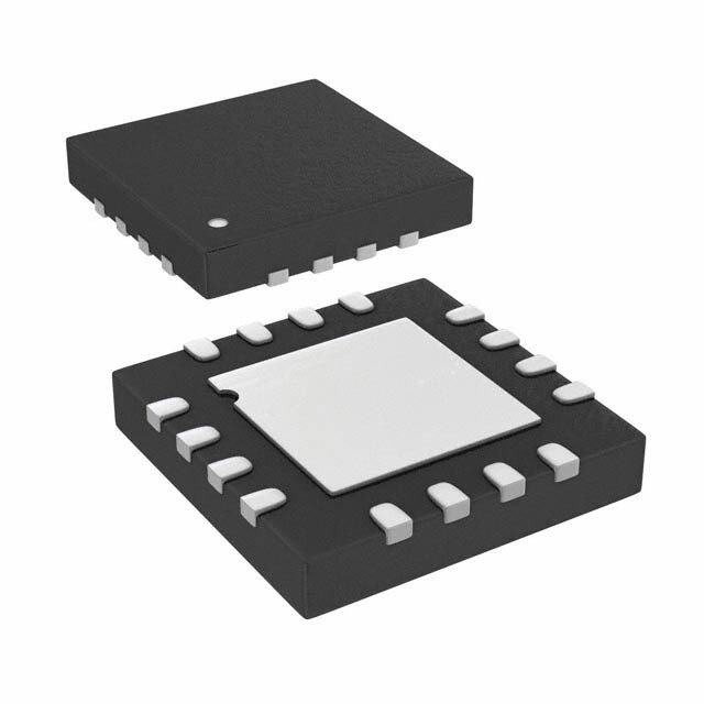
SY88303BL 3.3V, 3.2Gbps CML Limiting Post Amplifier with Wide Loss-of-Signal Detection Range General Description Features The SY88303BL low-power limiting post amplifiers are • Loss-of-signal detection circuit optimized to detect a designed for use in fiber-optic receivers. These devices wide input range connect to typical transimpedance amplifiers (TIAs). The • Chatter-free Open-Collector TTL Loss-of-Signal linear signal output from TIAs can contain significant (LOS) output amounts of noise and may vary in amplitude over time. • Single 3.3V power supply The SY88303BL quantizes these signals and output CML-level waveforms. • 155Mbps to 3.2Gbps operation • Low-noise CML data outputs The SY88303BL operates from a single +3.3V power supply, over temperatures ranging from –40oC to +85oC. • Programmable LOS level set (LOS ) LVL With their wide bandwidth and high gain, signals with • Available in a tiny 10-pin EPAD-MSOP and 16-pin data rates up to 3.2Gbps, and as small as 10mVPP, can QFN package be amplified to drive devices with CML/PECL inputs. The device generates a loss-of-signal (LOS) open- Applications collector TTL output. The LOS function is optimized to • PON detect a wide input range, as shown in the typical • Gigabit Ethernet operating characteristic curve on Page 6. A programmable loss-of-signal level-set pin (LOS ) sets • 1X and 2X Fibre Channel LVL the sensitivity of the input amplitude detection. • SONET/SDH: OC 3/12/24/48 – STM 1/4/8/16 LOS asserts high if the input amplitude falls below the • High-gain line driver and line receiver threshold sets by LOS and de-asserts low otherwise. LVL The enable bar input (/EN) de-asserts the true output Markets signal without removing the input signal. The LOS • FTTX output can be fed back to the /EN input to maintain output stability under a loss-of-signal condition. • Optical transceivers Typically, 3.5dB LOS hysteresis is provided to prevent • Datacom/Telecom chattering. • Low-gain TIA interface Datasheet and support documentation can be found on • Long-reach FOM Micrel’s web site at: www.micrel.com. Micrel Inc. • 2180 Fortune Drive • San Jose, CA 95131 • USA • tel +1 (408) 944-0800 • fax + 1 (408) 474-1000 • http:www.micrel.com November 2007 M9999-110207-A hbwhelp@micrel.com or (408) 955-1690
Micrel, Inc. SY88303BL Typical Application Pin Configuration 10-Pin EPAD-MSOP (K10-2) 16-Pin QFN Ordering Information Package Operating Lead Part Number Package Marking Type Range Finish Matte-Sn SY88303BLEY K10-2 Industrial 303B with Pb-Free bar line indicator Pb-free SY88303BLEYTR(1) K10-2 Industrial 303B with Pb-Free bar line indicator Matte-Sn Pb-free NiPdAu SY88303BLMG QFN-16 Industrial 303B with Pb-Free bar line indicator Pb-free SY88303BLMGTR(1) QFN-16 Industrial 303B with Pb-Free bar line indicator NiPdAu Pb-free Note: 1. Tape and Reel. November 2007 2 M9999-110207-A hbwhelp@micrel.com or (408) 955-1690
Micrel, Inc. SY88303BL Pin Description Pin Number Pin Number Pin Name Type Pin Function (MSOP) (QFN) TTL Input: 1 15 /EN Enable bar: De-asserts true data output when High. Default is low. 2 1 DIN Data Input True data input with 50Ω termination to VREF. 3 4 /DIN Data Input Complementary data input w50Ω termination to VREF. 4 6 VREF Reference Voltage: Placing a capacitor here to VCC helps stabilize. Loss-of-Signal Level Set: A resistor from this pin to VCC 5 14 LOSLVL Input sets the threshold for the data input amplitude at which the LOS output will be asserted. 6 2, 3, 10, 11 Device ground. Exposed pad must be connected to GND Ground Exposed Pad Exposed Pad PCB ground plane. Loss-of-Signal: Asserts high when the data input Open Collector amplitude falls below the threshold sets by LOSLVL. 7 7 LOS TTL Output For proper operation, install an external 4.75kΩ pull-up resistor at this output. 8 9 /DOUT CML Output Complementary data output. 9 12 DOUT CML Output True data output. 10 5, 8, 13, 16 VCC Power Supply Positive power supply. November 2007 3 M9999-110207-A hbwhelp@micrel.com or (408) 955-1690
Micrel, Inc. SY88303BL (1) (2) Absolute Maximum Ratings Operating Ratings Supply Voltage (V ) .................................... 0V to +4.0V Supply Voltage (V )............................ +3.0V to +3.6V CC CC Input Voltage (DIN, DIN) .................................... 0 to V Ambient Temperature (T ) .................. –40°C to +85°C CC A Output Current (I ) Junction Temperature (T ) ................ –40°C to +125°C OUT J Continuous ..................................................... +50mA Junction Thermal Resistance(3) Surge ........................................................... +100mA EPAD-MSOP /EN Voltage ........................................................ 0 to V θ (Still-Air) ............................................... 38oCW CC JA VREF Current ....................................... -800µA to +500µA ψJB ............................................................. 22oCW LOS Voltage .............................................. V to V LVL REF CC QFN Lead Temperature (soldering, 20sec.) .................. 260°C θ (Still-Air) ............................................... 61oCW Storage Temperature (T ) ..................... -65°C to +150°C JA s ψ ............................................................. 38oCW JB DC Electrical Characteristics V = 3.0V to 3.6V; R = 50Ω to V ; T = –40°C to +85°C; typical values at V = 3.3V, T = 25oC. CC L CC A CC A Symbol Parameter Condition Min Typ Max Units ICC Power Supply Current No output load 38 60 mA VLOSLVL LOSLVL Voltage VREF VCC V VOH CML Output HIGH Voltage VCC-0.020 VCC-0.005 VCC V VOL CML Output LOW Voltage VCC-0.475 VCC-0.4 VCC-0.350 V VOFFSET Differential Output Offset +80 mV VREF Reference Voltage VCC-1.48 VCC-1.32 VCC-1.16 V ZI Single-Ended Input Impedance 40 50 60 Ω TTL DC Electrical Characteristics V = 3.0V to 3.6V; T = –40°C to +85°C. CC A Symbol Parameter Condition Min Typ Max Units VIH /EN Input HIGH Voltage 2.0 V VIL /EN Input LOW Voltage 0.8 V IIH /EN Input HIGH Current VIN = 2.7V 20 µA VIN = VCC 100 µA IIL /EN Input LOW Current VIN = 0.5V -300 µA IOH LOS Output Leakage VOH = 3.6V 100 µA VOL LOS Output LOW Level IOL = +4mA 0.5 V Notes: 1. Permanent device damage may occur if absolute maximum ratings are exceeded. This is a stress rating only and functional operation is not implied at conditions other than those detailed in the operational sections of this data sheet. Exposure to absolute maximum rating conditions for extended periods may affect device reliability. 2. The data sheet limits are not guaranteed if the device is operated beyond the operating ratings. 3. Thermal performance assumes the use of a 4-layer PCB. Exposed pad must be soldered (or equivalent) to the device’s most negative potential on the PCB. November 2007 4 M9999-110207-A hbwhelp@micrel.com or (408) 955-1690
Micrel, Inc. SY88303BL AC Electrical Characteristics V = 3.0V to 3.6V; R = 50Ω to V ; T = –40°C to +85°C; typical values at V = 3.3V, T = +25°C. CC L CC A CC A Symbol Parameter Condition Min Typ Max Units tr, tf Output Rise/Fall Time Note 4 60 120 ps (20% to 80%) tJITTER Deterministic Note 5 15 psPP Random Note 6 5 psRMS VID Differential Input Voltage Swing Figure 1 10 1800 mVPP VOD Differential Output Voltage Swing VID > 12mVPP, Figure 1 700 800 950 mVPP TOFF LOS De-assert Time 2 10 µs TON LOS Assert Time 2 10 µs LOSDL Low LOS De-assert Level R = 15kΩ, Note 8 27 mVPP LOSAL Low LOS Assert Level R = 15kΩ, Note 8 18 mVPP HYSL Low LOS Hysteresis R = 15kΩ, Note 7 3.4 dB LOSDM Medium LOS De-assert Level R = 5kΩ, Note 8 53 80 mVPP LOSAM Medium LOS Assert Level R = 5kΩ, Note 8 21 36 mVPP HYSM LOS Hysteresis R = 5kΩ, Note 7 2 3.5 6 dB LOSDH High LOS De-assert Level R = 100Ω, Note 8 137 200 mVPP LOSAH High LOS Assert Level R = 100Ω, Note 8 70 94 mVPP HYSH High LOS Hysteresis R = 100Ω, Note 7 2 3.5 6 dB B-3dB 3dB Bandwidth 2 GHz AV(Diff) Differential Voltage Gain 39 dB S21 Single-ended Small-Signal Gain 26 33 dB Notes: 4. Amplifier in limiting mode. Input is a 200MHz, 100mVPP square wave. 5. Deterministic jitter measured using 3.2Gbps K28.5 pattern, VID = 10mVPP. 6. Random jitter measured using 3.2Gbps K28.7 pattern, VID = 10mVPP. 7. This specification defines electrical hysteresis as 20log (LOS De-assert/LOS Assert). The ratio between optical hysteresis and electrical hysteresis is found to vary between 1.5 and 2, depending upon the level of received optical power and ROSA characteristics. Based upon that ratio, the optical hysteresis corresponding to the electrical hysteresis range 2dB-6dB, shown in the AC characteristics table, will be 1dB-3dB Optical Hysteresis. 8. See “Typical Operating Characteristics” for a graph showing how to choose a particular RLOSLVL for a particular LOS assert and its associated de-assert amplitude. November 2007 5 M9999-110207-A hbwhelp@micrel.com or (408) 955-1690
Micrel, Inc. SY88303BL Typical Operating Characteristics Functional Characteristics November 2007 6 M9999-110207-A hbwhelp@micrel.com or (408) 955-1690
Micrel, Inc. SY88303BL Functional Block Diagram Detailed Description Loss-of-Signal The SY88303BL generates a chatter-free LOS open- The SY88303BL low-power limiting post amplifiers collector TTL output, as shown in Figure 4. LOS is used operate from a single +3.3V power supply, over temperatures from –40oC to +85oC. Signals with data to determine that the input amplitude is large enough to be considered a valid input. LOS asserts high if the input rates up to 3.2Gbps and as small as 10mV can be PP amplitude falls below the threshold sets by LOS and amplified. Figure 1 shows the allowed input voltage LVL de-asserts low otherwise. LOS can be fed back to the swing. The SY88303BL generates a LOS output enable bar (/EN) input to maintain output stability under allowing feedback to /EN for output stability. LOS sets LVL a loss-of-signal condition. /EN de-asserts the true output the sensitivity of the input amplitude detection. signal without removing the input signals. Input Amplifier Buffer Loss-of-Signal Level Set Figure 2 shows a simplified schematic of the input Programmable LOS level-set pin (LOS ) sets the stage. The high-sensitivity of the input amplifier allows LVL threshold of the input amplitude detection. Connecting signals as small as 10mV to be amplified. The input PP an external resistor between V and LOS set the amplifier also allows input signals as large as CC LVL voltage at LOS . This voltage ranges from V to V . 1800mV . Input signals below 12mVpp are linearly LVL CC REF PP The external resistor creates a voltage divider between amplified with a typical 42dB differential voltage gain. V and V , as shown in Figure 5. Since it is a limiting amplifier, these devices output CC REF typically 800mV voltage-limited waveforms for input Hysteresis PP signals greater than 12mV . Applications requiring the The SY88303BL typically provides 3.5dB LOS electrical PP SY88303BL to operate with strong signals should have hysteresis. By definition, a power ratio measured in dB the upstream TIA placed as close as possible to the is 10log (power ratio). Power is calculated as V2 / R for IN devices’ input pins. This ensures the best performance an electrical signal. Hence, the same ratio can be stated of the device. as 20log (voltage ratio). While in linear mode, the Output Buffer electrical voltage input changes linearly with the optical power and therefore, the ratios change linearly. Thus, The SY88303BL CML output buffers are designed to the optical hysteresis in dB is half the electrical drive 50Ω lines. The output buffer requires appropriate hysteresis in dB given in the data sheet. Since the termination for proper operation. An exterΩna l 50 SY88303BL is an electrical device, this data sheet refers resistor to V for each output pin provides this. Figure 3 CC to hysteresis in electrical terms. With 3.5dB LOS shows a simplified schematic of the output stage. hysteresis, a voltage factor of 1.5 is required to assert or de-assert LOS. November 2007 7 M9999-110207-A hbwhelp@micrel.com or (408) 955-1690
Micrel, Inc. SY88303BL Figure 1. VIS and VID Figure 2. Input Structure Figure 3. Output Structure Figure 4. LOS Output Structure Figure 5. LOSLVL Setting Circuit November 2007 8 M9999-110207-A hbwhelp@micrel.com or (408) 955-1690
Micrel, Inc. SY88303BL Package Information 10-Pin EPAD-MSOP (K10-2) November 2007 9 M9999-110207-A hbwhelp@micrel.com or (408) 955-1690
Micrel, Inc. SY88303BL 16-Pin QFN PCB Thermal Consideration for 16-Pin QFN® Package (Always solder, or equivalent, the exposed pad to the PCB) Package Notes: 1. Package meets Level 2 qualification. 2. All parts are dry-packaged before shipment. 3. Exposed pad must be soldered to a ground for proper thermal management, solder void has to be less than 50% of the epad area. November 2007 10 M9999-110207-A hbwhelp@micrel.com or (408) 955-1690
Micrel, Inc. SY88303BL MICREL, INC. 2180 FORTUNE DRIVE SAN JOSE, CA 95131 USA TEL +1 (408) 944-0800 FAX +1 (408) 474-1000 WEB http:www.micrel.com The information furnished by Micrel in this data sheet is believed to be accurate and reliable. However, no responsibility is assumed by Micrel for its use. Micrel reserves the right to change circuitry and specifications at any time without notification to the customer. Micrel Products are not designed or authorized for use as components in life support appliances, devices or systems where malfunction of a product can reasonably be expected to result in personal injury. Life support devices or systems are devices or systems that (a) are intended for surgical implant into the body or (b) support or sustain life, and whose failure to perform can be reasonably expected to result in a significant injury to the user. A Purchaser’s use or sale of Micrel Products for use in life support appliances, devices or systems is a Purchaser’s own risk and Purchaser agrees to fully indemnify Micrel for any damages resulting from such use or sale. © 2007 Micrel, Incorporated. November 2007 11 M9999-110207-A hbwhelp@micrel.com or (408) 955-1690
Mouser Electronics Authorized Distributor Click to View Pricing, Inventory, Delivery & Lifecycle Information: M icrel: SY88303BLMG TR M icrochip: SY88303BLMG SY88303BLEY SY88303BLEY-TR SY88303BLMG-TR

 Datasheet下载


