ICGOO在线商城 > 射频/IF 和 RFID > RF 发射器 > SX1230I066TRT
 Datasheet下载
- 型号: SX1230I066TRT
- 制造商: SEMTECH
- 库位|库存: xxxx|xxxx
- 要求:
| 数量阶梯 | 香港交货 | 国内含税 |
| +xxxx | $xxxx | ¥xxxx |
查看当月历史价格
查看今年历史价格
SX1230I066TRT产品简介:
ICGOO电子元器件商城为您提供SX1230I066TRT由SEMTECH设计生产,在icgoo商城现货销售,并且可以通过原厂、代理商等渠道进行代购。 SX1230I066TRT价格参考。SEMTECHSX1230I066TRT封装/规格:RF 发射器, RF Transmitter ISM 315MHz, 434MHz, 868MHz, 915MHz 17dBm 600kbps PCB, Surface Mount Antenna 24-VFQFN Exposed Pad。您可以下载SX1230I066TRT参考资料、Datasheet数据手册功能说明书,资料中有SX1230I066TRT 详细功能的应用电路图电压和使用方法及教程。
| 参数 | 数值 |
| 产品目录 | |
| 描述 | IC TX UHF 433/868/916 MHZ 24-QFN |
| 产品分类 | |
| 品牌 | Semtech |
| 数据手册 | |
| 产品图片 |
|
| 产品型号 | SX1230I066TRT |
| PCN设计/规格 | |
| rohs | 无铅 / 符合限制有害物质指令(RoHS)规范要求 |
| 产品系列 | - |
| 产品目录页面 | |
| 其它名称 | SX1230I066CT |
| 功率-输出 | 17dBm |
| 包装 | 剪切带 (CT) |
| 天线连接器 | PCB,表面贴装 |
| 存储容量 | - |
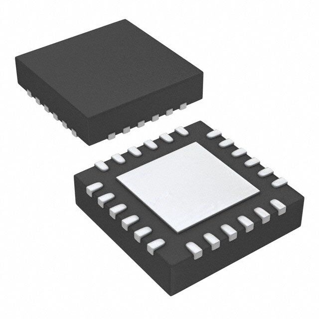
| 封装/外壳 | 24-MLPQ |
| 工作温度 | -40°C ~ 85°C |
| 应用 | RKE |
| 数据接口 | PCB,表面贴装 |
| 数据速率(最大值) | 600kbps |
| 标准包装 | 1 |
| 特性 | - |
| 特色产品 | http://www.digikey.com/cn/zh/ph/semtech/sx1230.html |
| 电压-电源 | 1.8 V ~ 3.7 V |
| 电流-传输 | 95mA |
| 调制或协议 | ISM |
| 频率 | 315MHz,434MHz,868MHz,915MHz |


- 商务部:美国ITC正式对集成电路等产品启动337调查
- 曝三星4nm工艺存在良率问题 高通将骁龙8 Gen1或转产台积电
- 太阳诱电将投资9.5亿元在常州建新厂生产MLCC 预计2023年完工
- 英特尔发布欧洲新工厂建设计划 深化IDM 2.0 战略
- 台积电先进制程称霸业界 有大客户加持明年业绩稳了
- 达到5530亿美元!SIA预计今年全球半导体销售额将创下新高
- 英特尔拟将自动驾驶子公司Mobileye上市 估值或超500亿美元
- 三星加码芯片和SET,合并消费电子和移动部门,撤换高东真等 CEO
- 三星电子宣布重大人事变动 还合并消费电子和移动部门
- 海关总署:前11个月进口集成电路产品价值2.52万亿元 增长14.8%


PDF Datasheet 数据手册内容提取
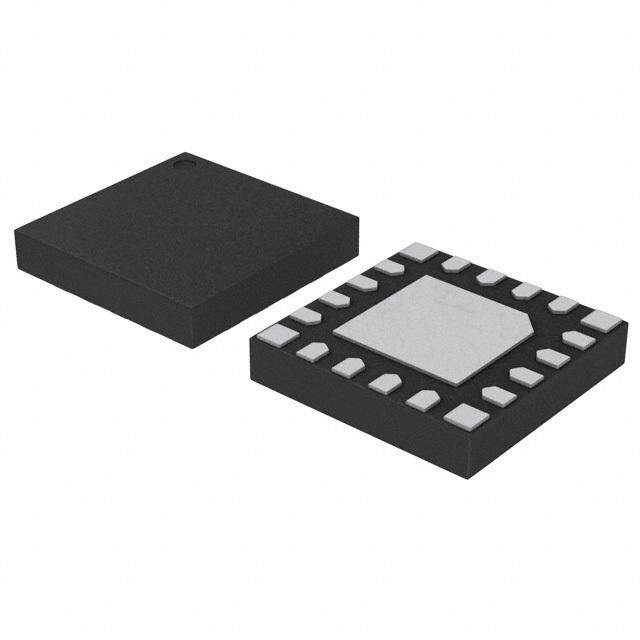
SX1230 ADVANCED COMMUNICATIONS & SENSING DATASHEET SX1230 - Integrated Transmitter IC Narrow/wideband 315 MHz, 434 MHz 868 MHz and 915 MHz band Transmitter GENERAL DESCRIPTION APPLICATIONS The SX1230 is a fully integrated transmitter which can Remote Keyless Entry (RKE) operate in the 315, 434, 868 and 915 MHz licence free ISM bands. Remote Control / Security Systems The transmitter has two modes of operation, a conventional Voice and Data RF Communication Links MCU controlled mode and a ‘stand-alone’ mode which Process and building / home control enables the SX1230 to download configuration and messages from an E2PROM in response to a user input. Active RFID Stand-alone mode makes the SX1230 ideal for miniaturized AMR / AMI Platforms or low cost remote keyless entry (RKE) applications. It also offers the unique advantage of narrow-band and wide-band KEY PRODUCT FEATURES communication in a range of modulation formats. The SX1230 offers high RF output power and channelized +17 dBm to -18 dBm Programmable output power. operation suited for the European (ETSI EN 300-220-1), Bit rates up to 600 kbits / sec. North American (FCC part 15.231, 15.247 and 15.249) and FSK, GFSK, MSK, GMSK and OOK modulation. Japanese (ARIB T-67) regulatory standards. Stand-alone mode: No need for a host MCU. ORDERING INFORMATION Consistent RF performance over a 1.8 to 3.7 V range. Low phase noise (-95 dBc/Hz at 50 kHz) with automated Part Number Temperature Range Qty. per Reel Package PLL calibration and fully integrated VCO and loop filter. SX1230I066TRT -40 °C to +85 °C 3000 MLPQ-24 (4x4mm) On chip RC timer for timer / wake-up applications. Low battery detection. Pb-free, Halogen free, RoHS/WEEE compliant product MLPQ-24 4x4mm Package - Operating Range [-40;+85°C] S U _ 1 0 _ 2 0 0 0 T S 1SX1230, Revision 4 December 2015 Page 1 www.semtech.com ©1.2015 Semtech Corp.
SX1230 ADVANCED COMMUNICATIONS & SENSING DATASHEET Table of contents Section Page 1. General Description..................................................................................................................................................4 1.1. Simplified Block Diagram..................................................................................................................................4 1.2. Pin Diagram......................................................................................................................................................5 1.3. Pin Description.................................................................................................................................................6 2. Electrical Characteristics..........................................................................................................................................7 2.1. ESD Notice.......................................................................................................................................................7 2.2. Absolute Maximum Ratings..............................................................................................................................7 2.3. Operating Range...............................................................................................................................................7 2.4. Electrical Specifications....................................................................................................................................8 3. Timing Characteristics..............................................................................................................................................9 4. Working Modes of the SX1230...............................................................................................................................10 4.1. Operating Modes............................................................................................................................................10 4.2. Application Modes...........................................................................................................................................10 4.2.1. Stand Alone Mode.................................................................................................................................. 10 4.2.2. MCU Mode...............................................................................................................................................11 5. Operation of the SX1230........................................................................................................................................12 5.1. Main Parameters............................................................................................................................................ 12 5.1.1. Center Frequency................................................................................................................................... 12 5.1.2. Frequency Deviation............................................................................................................................... 12 5.1.3. Bit Rate................................................................................................................................................... 12 5.2. Synthesizer.................................................................................................................................................... 13 5.3. The Power Amplifier....................................................................................................................................... 14 6. Digital Control and Interface.................................................................................................................................. 15 6.1. Stand Alone Mode......................................................................................................................................... 15 6.1.1. State Machine Description...................................................................................................................... 15 6.1.2. Memory Organization of the E2PROM................................................................................................... 15 6.1.3. Periodic mode......................................................................................................................................... 17 6.1.4. Low Battery Indicator: Stand Alone Mode............................................................................................... 18 6.1.5. Low Battery Indicator: MCU Mode.......................................................................................................... 18 6.2. MCU Mode..................................................................................................................................................... 18 6.2.1. SPI Operation......................................................................................................................................... 18 6.2.2. Data and Data Clock Usage....................................................................................................................20 6.3. SX1230 Register Description........................................................................................................................21 7. SX1230 Application Circuits...................................................................................................................................27 7.1. SX1230 E2PROM Mode Application Circuit...................................................................................................27 7.2. SX1230 MCU Mode Application Circuit..........................................................................................................28 7.3. Complete RKE Application Circuit..................................................................................................................28 S U _ 1 0 _ 2 0 0 0 T S SX1230, Revision 4 December 2015 Page 2 www.semtech.com ©2015 Semtech Corp.
SX1230 ADVANCED COMMUNICATIONS & SENSING DATASHEET Table of contents Section Page 7.4. Wake-up Times.............................................................................................................................................. 29 7.5. Reset Pin Timing............................................................................................................................................ 29 7.6. Operation with 17 dBm Output Power............................................................................................................31 7.7. Matching for 13 dBm Output Power and Below............................................................................................. 33 7.8. TCXO Connection.......................................................................................................................................... 34 7.9. PCB Layout Considerations........................................................................................................................... 34 8. Reference Design.................................................................................................................................................. 35 9. Reference Design Performance............................................................................................................................ 36 9.1. Power Output versus Consumption............................................................................................................... 36 9.2. Power Output Flatness versus Temperature and Supply Voltage................................................................. 37 9.3. Phase Noise....................................................................................................................................................38 9.4. SX1230 Baseband Filtering............................................................................................................................40 9.5. Adjacent Channel Power................................................................................................................................40 10. Packaging Information............................................................................................................................................43 11. Package Marking....................................................................................................................................................43 12. Recommended PCB Land Pattern.........................................................................................................................44 13. Soldering Profile......................................................................................................................................................45 S U _ 1 0 _ 2 0 0 0 T S SX1230, Revision 4 December 2015 Page 3 www.semtech.com ©2015 Semtech Corp.
SX1230 Integrated Transmitter IC ADVANCED COMMUNICATIONS & SENSING DATASHEET This product datasheet contains a detailed description of the SX1230 performance and functionality. Please consult the Semtech website for the latest updates or errata (www.semtech.com). 1. General Description The SX1230 is a multi-band, single chip transmitter IC capable of (G)FSK, (G)MSK, and OOK modulation of an input data stream. It can transmit this modulated signal in any of the license free ISM bands from 290 MHz to 1020 MHz. 1.1. Simplified Block Diagram Figure 1. SX1230 Simplified Block Diagram The general architecture of the SX1230 is shown in Figure 1. The frequency synthesizer generating the LO frequency is a third-order fractional-N sigma-delta PLL. The PLL is capable of fast auto-calibration and offers fast switching and settling times. For frequency modulation ((G)FSK and (G)MSK), the modulation is performed within the PLL bandwidth. Optional pre-filtering of the bit stream may also be enabled to reduce the power delivered to adjacent channels. Amplitude modulation (OOK), is performed via a DAC driving the reference of the regulator of the PA. Note that pre-filtering of the bit stream is also available in this mode. The VCO works at 2, 4 or 6 times the RF output frequency to improve the quadrature precision and reduce pulling effects during transmission. The PA of the SX1230 is comprised of two amplifiers - one high power, one low power. This enables the SX1230 to deliver a wide range, over 30 dB, of output powers - up to +13 dBm in single PA configuration. However, with an appropriate output S U _ impedance transformation, in dual PA mode, this can be increased to +17 dBm. 1 0 _ 2 0 0 0 T S SX1230, Revision 4 December 2015 Page 4 www.semtech.com ©2015 Semtech Corp.
SX1230 Integrated Transmitter IC ADVANCED COMMUNICATIONS & SENSING DATASHEET The SX1230 also includes two timing references; an RC oscillator, for sleep mode operation of the SPI interface (in MCU mode), and a 32 MHz crystal oscillator, which serves as the low-noise frequency reference of the PLL. The references and supply voltages are provided by the power distribution system which includes several regulators allowing true battery powered operation. 1.2. Pin Diagram The following diagram shows the pinouts of the 4x4 mm MLPQ-24 package. Figure 2. SX1230 Pin diagram (top view) S U _ 1 0 _ 2 0 0 0 T S SX1230, Revision 4 December 2015 Page 5 www.semtech.com ©2015 Semtech Corp.
SX1230 Integrated Transmitter IC ADVANCED COMMUNICATIONS & SENSING DATASHEET 1.3. Pin Description Table 1 Description of the SX1230 Pinouts Number Name Type Description MCU Mode Description Stand Alone Mode 0 GROUND - Global ground (bottom of package) 1 E2_MODE I Mode select ‘0’ = MCU mode Mode select ’1’ = Stand alone mode 2 VR_ANA I/O Regulated supply voltage for analog circuitry 3 XTB I/O Crystal connection 4 XTA I Crystal connection 5 RESET I/O Reset, active high 6 PB(0) I Low battery indicator output Push-button input 0, active high 7 PB(1) I Connect to GROUND Push-button input 1, active high 8 PB(2) I Connect to GROUND Push-button input 2, active high 9 PB(3) I Connect to GROUND Push-button input 3, active high 10 VR_DIG I Regulated supply for digital circuitry 11 CLKOUT O Reference clock output for MCU Reference clock output 12 PLL_LOCK O PLL lock detection, active high Transmission of frame OK, active low 13 DCLK O Output data clock NC 14 DATA I Modulation input data NC 15 SCK I SPI Clock input SPI Clock output 16 MISO I/O SPI Data output SPI Data input 17 MOSI I/O SPI Data input SPI Data output 18 NSS I/O SPI Chip select input SPI Chip select output 19 TEST I Connect to GROUND 20 GND - RF Ground 21 RFOUT O RF Output 22 GND - RF Ground 23 VR_PA I/O Regulated supply for PA 24 VBAT I Main supply voltage from battery S U _ 1 0 _ 2 0 0 0 T S SX1230, Revision 4 December 2015 Page 6 www.semtech.com ©2015 Semtech Corp.
SX1230 Integrated Transmitter IC ADVANCED COMMUNICATIONS & SENSING DATASHEET 2. Electrical Characteristics 2.1. ESD Notice The SX1230 is an electrostatic discharge sensitive device. It satisfies: Class 1C of the JEDEC standard JESD22-A114-B (human body model) on pins 2, 10, 21 and 23. Class 2 of the JEDEC standard JESD22-A114-B (human body model) on all other pins. 2.2. Absolute Maximum Ratings Stresses above the values listed below may cause permanent device failure. Exposure to absolute maximum ratings for extended periods may affect device reliability. Table 2 Absolute Maximum Ratings Symbol Description Min Max Unit VDDmr Supply Voltage -0.5 3.9 V Tmr Temperature -55 115 ° C 2.3. Operating Range Operating ranges define the limits for functional operation and the parametric characteristics of the device as described in this section. Functionality outside these limits is not implied. Table 3 Operating Range Symbol Description Min Max Unit VDDop Supply voltage 1.8 3.7 V Top Operational temperature range -40 85 ° C Clop Load capacitance on digital ports - 25 pF S U _ 1 0 _ 2 0 0 0 T S SX1230, Revision 4 December 2015 Page 7 www.semtech.com ©2015 Semtech Corp.
SX1230 Integrated Transmitter IC ADVANCED COMMUNICATIONS & SENSING DATASHEET 2.4. Electrical Specifications The table below gives the electrical specifications of the transmitter under the following conditions: Supply voltage = 3.3 V, temperature = 25 °C, f = 32 MHz, f = 915 MHz, 2-level FSK modulation without prefiltering, Df = 5 kHz, bit rate = 4.8 XOSC RF kbit/s and output power = 13 dBm terminated in a matched 50 ohm impedance, unless otherwise specified. Table 4 Transmitter Specifications Symbol Description Conditions Min Typ Max Unit Current Consumption IDDSL Supply current in sleep mode - 0.5 1 μA IDDST Supply current in standby mode Crystal oscillator enabled - 0.9 1.2 mA IDDFS Supply current in synthesiser - 8 - mA mode IDDT Supply current in transmit mode RF Power o/p = 17 dBm - 95 - mA with appropriate external match- RF Power o/p = 13 dBm - 45 - mA ing (see Section 7). RF Power o/p = 10 dBm - 33 40 mA RF Power o/p = 0 dBm - 20 25 mA RF and Baseband Specifications BRF Bit rate, FSK Programmable. 1.2 - 600 kbps BRO Bit rate, OOK Programmable. 1.2 - 32 kbps FDA Frequency deviation, FSK Programmable 0.6 - 300 kHz RFOP RF output power in 50 ohms Programmable with 1 dB steps. Max 10 13 - dBm Min -21 -18 - dBm PHN Transmitter phase noise 50 kHz Offset from carrier - -95 - dBc/ Hz RFOPH Max RF output power with an With external match to 50 ohms. 14 17 - dBm external impedance transforma- tion ACP Transmitter adjacent channel Pre-filter enabled. Measurement - - -37 dBm power (measured at 25 kHz off- conditions as defined by EN 300 set) 220-1 V2.1.1. FR Synthesizer Frequency Range Programmable. FBand 1 290 - 340 MHz FBand 2 431 - 510 MHz FBand 3 862 - 1020 MHz FSTEP Frequency synthesizer step FXOSC/219 - 61 - Hz FRC RC Oscillator frequency range 45 65 85 kHz Timing Specifications S U _ 01 TS_FS Frequency synthesizer wake up Crystal oscillator Enabled. - 100 150 μs _ 02 time 0 0 T S SX1230, Revision 4 December 2015 Page 8 www.semtech.com ©2015 Semtech Corp.
SX1230 Integrated Transmitter IC ADVANCED COMMUNICATIONS & SENSING DATASHEET Symbol Description Conditions Min Typ Max Unit TS_TR Transmitter wake-up time Frequency synthesizer enabled. - 120 - μs Note, depends upon bit rate and ramp time, please refer to Section 7.4. TS_OS Crystal oscillator wake-up time - 300 500 μs FXOSC Crystal oscillator frequency 26 32 32 MHz TS_TT Total Wake up time Sleep to transmit, automated. Note, - 450 - μs depends upon bit rate and ramp time, please refer to Section 7.4. T_DATA Data set-up time - - 0.25 μs 3. Timing Characteristics The following table gives the operating specifications for the SPI interface of the SX1230. Table 5 SPI Timing Specifications Symbol Description Conditions Min Typ Max Unit f SCK Frequency - - 10 MHz SCK t SCK High time 50 - - ns ch t SCK Low time 50 - - ns cl t SCK rise time - 5 - ns rise t SCK Fall time - 5 - ns fall tsetup MOSI Setup time From MOSI transition to SCK rising 30 - - ns edge t MOSI hold time From SCK rising edge to MOSI tran- 20 - - ns hold sition t NSS setup time From NSS falling edge to SCK rising 30 - ns nl edge t NSS Hold time From SCK falling edge to NSS rising 30 - - ns nh,n edge. For explanatory diagrams of the timing characteristic parameters, please see Figure 7 and Figure 8. S U _ 1 0 _ 2 0 0 0 T S SX1230, Revision 4 December 2015 Page 9 www.semtech.com ©2015 Semtech Corp.
SX1230 Integrated Transmitter IC ADVANCED COMMUNICATIONS & SENSING DATASHEET 4. Working Modes of the SX1230 4.1. Operating Modes The four operating modes of the SX1230 are shown in Table 6. Each of these may be selected via the SPI bus by writing the corresponding bits to Mode(2:0). A key feature of the SX1230 is that the transition from one operating mode to the next is automatically optimized. For example, if the transmit operating mode is selected whilst in sleep operating mode then, in a pre-defined time-optimized sequence, each of the intermediate modes is engaged sequentially without the need to issue any further SPI commands. For more information on timing and optimization please see Section 7.4. Table 6 SX1230 Operating Modes Enabled Blocks MODE(2:0) Selected Mode RC Osc SPI Xtal Osc Freq. Synth. PA 000 Sleep mode Optional x 001 Stand-by mode Optional x x 010 FS mode Optional x x x 011 Transmit mode Optional x x x x 4.2. Application Modes The SX1230 has two application modes, selected by applying an external logical level to the E2_MODE input (pin 6). The first, MCU mode (E2_Mode= ‘0’), configures the SX1230 as an SPI slave. This permits the configuration of the circuit by an external microprocessor via the SPI interface of the SX1230 and the data to be applied via the DATA input (pin 14). The second application mode, stand-alone mode (E2_Mode = 0), sees the SX1230 configured as SPI master. In the stand- alone application mode the SX1230 can download its configuration from an external SPI E2PROM. Moreover, in response to an input on the GPIO pins, a specific configuration can be programmed and a payload transmitted. Note that this mode selection process is performed at start up (or POR) of the circuit. Thus the hardware mode cannot be dynamically changed without resetting the chip. This may be achieved either by power down or by issuing an active high POR signal to the Reset input (pin 5). For reset signal timing please see the diagram of Figure 13 and accompanying description. 4.2.1. Stand Alone Mode In stand alone mode (E2_Mode = ‘1’) the SX1230 will operate as a stand-alone SPI master which can download both register settings and data payload from an SPI E2PROM. Four debounced GPIO inputs are available in stand alone mode, in this application mode the SX1230 remains in sleep operating mode until either a single or combination of button presses are detected. SX1230 can then be dynamically reconfigured and / or transmit a data sequence stored within the E2PROM. The SX1230 can accommodate SPI E2PROM sizes up to 8 kbit and uses industry standard SPI commands. For a full description of E2PROM use with SX1230 and the associated application circuits, please see Section 6.1. The application circuit for stand-alone operation is shown in Figure 3, note that both matching and L are band specific whilst C is M TX application specific. S U _ 1 0 _ 2 0 0 0 T S SX1230, Revision 4 December 2015 Page 10 www.semtech.com ©2015 Semtech Corp.
SX1230 Integrated Transmitter IC ADVANCED COMMUNICATIONS & SENSING DATASHEET Figure 3. SX1230 Stand-Alone Application Circuit 4.2.2. MCU Mode The SX1230 is also capable of operating in a conventional MCU controlled mode. Figure 4 shows the SX1230 operating in MCU mode and connected to an external microcontroller. Note that CLKOUT provides the oscillator signal for the MCU, thus negating the need for two crystal oscillators. The DCLK connection is also optional - only being required if the data rate is to be determined by SX1230 or transmit filtering is to be used. S U _ 1 Figure 4. SX1230 MCU Mode Application Circuit 0 _ 2 0 0 0 T S SX1230, Revision 4 December 2015 Page 11 www.semtech.com ©2015 Semtech Corp.
SX1230 Integrated Transmitter IC ADVANCED COMMUNICATIONS & SENSING DATASHEET 5. Operation of the SX1230 The SX1230 is an integrated ISM band transmitter and features a fully integrated frequency synthesizer, modulator and power amplifier. This section describes the operation of the SX1230 and the functionality of these blocks. 5.1. Main Parameters 5.1.1. Center Frequency The carrier output center frequency, f , of the SX1230 is programmable via the SPI interface. It is determined by the RF following equation: freq_rf(23:0) f f = -----------------------------------------X---O----S--C--- RF 19 2 where freq_rf(23:0) is the decimal value of the 24 bit number stored in configuration registers FrfMsb, FrfMid and FrfLsb and f is the frequency of the crystal oscillator. If the optimal value of 32 MHz is selected for the crystal oscillator, then XOSC this results in a programmable frequency resolution of 61.035 Hz. Note that RF output frequencies are only valid in the bands 290-340 MHz, 431-510 MHz and 862-1020 MHz. Note also, that for ease of use, the band selection process is performed automatically. 5.1.2. Frequency Deviation The frequency deviation of the SX1230 in FSK mode is given by the following equation: f df_coeff(13:0) f = -----X---O----S---C----------------------------------------- 19 2 where df_coeff is the decimal value of the 14 bit contents of the FdevLsb and FdevMsb configuration registers. 5.1.3. Bit Rate The bit rate (or, depending upon coding, the chip rate) of the SX1230 is given by the following equation: f R = -------------X---O----S---C---------- B br_ratio(15:0) where f is the crystal oscillator frequency, br_ratio is the decimal value of the 16 bit contents of registers BrMsb and XOSC BrLsb. Note that for OOK modulation the maximum bit rate is 32.7 kbps which corresponds to a br_ratio(15:0) of 979. The table below gives examples of some of the standard data rates accessible with SX1230. S U _ 1 0 _ 2 0 0 0 T S SX1230, Revision 4 December 2015 Page 12 www.semtech.com ©2015 Semtech Corp.
SX1230 Integrated Transmitter IC ADVANCED COMMUNICATIONS & SENSING DATASHEET Table 7 Example Standard Bitrates and their Corresponding Register Settings. Type BrMSB BrLSB (G)FSK, (G)MSK OOK Rb Actual (to 7s.f.) Classical modem baud rates 0x68 0x2B 1.2 kbps 1.2 kbps 1200.015 (multiples of 1.2 kbps) 0x34 0x15 2.4 kbps 2.4 kbps 2400.060 0x1A 0x0B 4.8 kbps 4.8 kbps 4799.760 0x0D 0x05 9.6 kbps 9.6 kbps 9600.960 0x06 0x83 19.2 kbps 19.2 kbps 19196.16 0x03 0x41 38.4 kbps 38415.36 0x01 0xA1 76.8 kbps 76738.60 0x00 0xD0 153.6 kbps 153846.1 Classical modem baud rates 0x02 0x2C 57.6 kbps 57553.95 (multiples of 0.9 kbps) 0x01 0x16 115.2 kbps 115107.9 Round bit rates 0x0A 0x00 12.5 kbps 12.5 kbps 12500.00 (multiples of 12.5, 25 and 50 kbps) 0x05 0x00 25 kbps 25 kbps 25000.00 0x80 0x00 50 kbps 50000.00 0x01 0x40 100 kbps 100000.0 0x00 0xD5 150 kbps 150234.7 0x00 0xA0 200 kbps 200000.0 0x00 0x80 250 kbps 250000.0 0x00 0x6B 300 kbps 299065.4 Watch Xtal frequency 0x03 0xD1 32.768 kbps 32.768 kbps 32753.32 5.2. Synthesizer The frequency synthesizer of the SX1230 is a fully integrated fractional-N third-order sigma-delta phase-locked loop and VCO. Also incorporated are fully integrated third-order and low pass filters which determine the loop bandwidth. All of these features are fully automated and derived from the user bitrate and frequency deviation settings, as described in Sections 5.1.1 to 5.1.3. To ensure the frequency accuracy of the PLL output it is necessary to perform calibration. The calibration process is performed automatically upon power up of the SX1230. However, the calibration feature is also accessible to the user via the SPI configuration register, PllStat (address 0x0A). The calibration is performed by setting bit 2 (pll_cal) high. This ensures that the frequency output accuracy is limited only by the frequency error of the crystal oscillator, the calibration procedure lasts 500 μs, during which time pll_cal_done (bit 4 of address 0x0A) is set low. Once complete pll_cal_done is S set high and confirmation of a successful calibration can be obtained by reading pll_cal_ok. U _ 1 0 _ 2 0 0 0 T S SX1230, Revision 4 December 2015 Page 13 www.semtech.com ©2015 Semtech Corp.
SX1230 Integrated Transmitter IC ADVANCED COMMUNICATIONS & SENSING DATASHEET 5.3. The Power Amplifier A simplified schematic of the dual power amplifiers of the SX1230 is shown in Figure 5. PA 1 comprises a pair of amplifiers: One dedicated for low power use, LPA, for programmed powers from -18 to -3 dBm: The second for high power use, HPA, for programmed powers from -2 to 13 dBm. PA 2 is a single high power amplifier and may be used in conjunction with PA 1 to deliver the full 17 dBm of output power. Figure 5. Simplified Schematic of the SX1230 Power Amplifier The mode of operation of the PA’s is determined by the register setting pa_select(1:0) which is configured as shown in Table 8, below. The output power of the PA is determined by the value of the register pow_val(4:0), with a single PA enabled the output power is set by: Pout = –18 dBm + pow_val(4:0) The default setting for this register is 13 dBm. The expressions for the output power with other combinations of power amplifier enabled are shown in Table 8. Note also that the power amplifier current limiter, over current protection (OCP), feature of SX1230 can also limit the output power. To ensure correct operation at 17 dBm ensure that trim_ocp(3:0) is set to 105 mA (‘1100’). Table 8 Power Amplifier Mode Selection Truth Table pa_select(1:0) Mode Power Range Pout Formula 00 invalid - 01 PA1 enabled -18 to 13 dBm -18 dBm + pow_val(4:0) 10 PA2 enabled - - 11 Dual PA -13 to 17 dBm -13 dBm + pow_val(4:0) The ramp and power control features of the PA, determine the regulator output voltage which is used to power the S U amplifiers, this must be done through an external RF choke. _ 1 0 _ 2 0 0 0 T S SX1230, Revision 4 December 2015 Page 14 www.semtech.com ©2015 Semtech Corp.
SX1230 Integrated Transmitter IC ADVANCED COMMUNICATIONS & SENSING DATASHEET 6. Digital Control and Interface The SX1230 has several operating modes, configuration parameters and internal status indicators which are stored in internal registers. In MCU mode, all of these registers can be accessed by an external microcontroller via the SPI interface. In stand alone mode, both the configuration information and the data to be transmitted, are stored in an external E2PROM. The way that both the configuration and payload information is stored in the E2PROM must match the way the configuration is defined in the internal registers. For a full description see Section 6.1.2. 6.1. Stand Alone Mode 6.1.1. State Machine Description The stand alone mode is activated when the pin E2_Mode is tied to VDD. The SX1230 SPI interface is then configured in master mode. The internal state machine of the SX1230 then carries out the following operations: 1) Immediately after power-up, the SPI interface reads the main configuration section in the E2PROM and then goes into the ‘sleep’ operating mode (i.e. all blocks off). 2) Whilst in ‘sleep’ operating mode, when an edge is detected on any of the push-buttons PB[3:0], the chip wakes-up and starts the RC oscillator (typical startup time ~100 μs). 3) The RC oscillator is used to clock a debounce timer which gives the logical push button input value after the programmed delay. The frame section corresponding to the button value (1 to 15) is read from the E2PROM. At this point additional, button specific, configuration information may be loaded. Otherwise, the configuration settings of 1) are used. Using the appropriate configuration, the payload corresponding to the detected button press is then transmitted. The payload transmission may be repeated up to 254 times. 4) When the frame has been transmitted, the pad PLL_LOCK goes low and the chip goes into SLEEP mode. 6.1.2. Memory Organization of the E2PROM The memory map for stand alone mode is shown in Figure 6. The configuration information occupies the first 77 bytes, the format of the configuration is {ADDR; VALUE} - therefore allowing up to 38 registers to be defined. Each push button configuration is mapped directly to a location in the E2PROM - determined by the mappings given in Table 9 and the variable section_size(5:0). The purpose of this variable, push button specific, section size is to allow the optimum use of different sizes of external memory. Note that the maximum frame length is 64 bytes - this equates to a maximum E2PROM size of 8 kbit. The influence of the section_size variable is illustrated in Figure 6. The mapping of Table 9 permits up to 15 frames to be defined. Each section may contain both write_registers commands and the payload to be transmitted. Thus allowing the dynamic configuration of settings such as output power and frequency in response to a button push. Each section within the E2PROM must conform to the following format: {FIFO_ADDR; REPEAT; LENGTH; VALUE_1; VALUE_2;...;VALUE_N}. Where VALUE_1... N is the user defined payload, REPEAT is the number of times the frame is to be transmitted, LENGTH defines the number of bytes in the message and FIFO_ADDR = 0x95. S U _ 1 0 The push-buttons may need to be debounced before being read. The debouncer time constant is programmed by the _ 2 0 debounce_time(2:0) register which allows a range of debounce timer values to be accessed from 470 ms to 480 ms. An 0 0 T S SX1230, Revision 4 December 2015 Page 15 www.semtech.com ©2015 Semtech Corp.
SX1230 Integrated Transmitter IC ADVANCED COMMUNICATIONS & SENSING DATASHEET option for no debouncing is also available. Note that time constants are process and temperature dependent and may vary by +/- 15%. Figure 6. Memory Mapping in Stand Alone Mode The table below gives the push button mappings for the determination of E2PROM memory locations. Note that the combinations PB[3:0] = ‘0001’, ‘0010’, ‘0100’ and ‘1000’ are mapped to the four lowest locations in memory. This mapping allows the use of a simple four button interface with the minimum memory size. Table 9 Push Button Combination to E2PROM Memory Location Mapping PB[3:0] PB_MAPPING(3:0) PB[3:0] PB_MAPPING(3:0) 0000 None (no active push-button) 1000 3 0001 0 1001 7 0010 1 1010 8 0011 4 1011 11 0100 2 1100 9 0101 5 1101 12 0110 6 1110 13 0111 10 1111 14 / Low Battery The commands in the E2PROM are written as instructions thus bit 7 is set high - equivalent to adding 0x80 to the register S address to be programmed. As was shown in Figure 6, the first 77 bytes are used for configuration. Note that registers only U _ require programming if they hold a value other than the default value (see table 11 for default register settings). 1 0 _ 2 0 0 0 T S SX1230, Revision 4 December 2015 Page 16 www.semtech.com ©2015 Semtech Corp.
SX1230 Integrated Transmitter IC ADVANCED COMMUNICATIONS & SENSING DATASHEET The following table gives an example snippet of E2PROM contents, here for each location in E2PROM memory the first 13 bytes of the available 77 (0x4C) bytes are occupied with configuration. The remaining bytes are left in their default 0xFF setting. The first push-button memory location is at 0x4D. Here we see that the periodic mode timer (see following section for a full description) is configured and a 10 byte payload follows. Subsequent push buttons are configured at the locations determined by the section size, see Figure 6. Table 10 Example External SPI E2PROM Contents for SX1230 Configuration Address Content Comment Address Content Comment 0x00 0x81 Start-up config. (address) 0x4C 0xFF Empty 0x01 0x05 Start-up config. (data) 0x4D 0x97 PB[0] config (address) 0x02 0x82 Start-up config. (address) 0x4E 0x00 PB[0] config (data) 0x03 0x00 Start-up config. (data) 0x4F 0x95 FIFO address 0x04 0x83 Start-up config. (address) 0x50 0x0A Repeat 0x05 0x03 Start-up config. (data) 0x51 0x0A Length 0x06 0x84 Start-up config. (address) 0x52 0x55 Start of PB[0] Payload 0x07 0x33 Start-up config. (data) 0x53 0x55 PB[0] Payload: Byte 1 0x08 0x85 Start-up config. (address) 0x54 0x55 PB[0] Payload: Byte 2 0x09 0xE3 Start-up config. (data) 0x55 0x55 PB[0] Payload: Byte 3 0x0A 0x90 Start-up config. (address) 0x56 0xAA PB[0] Payload: Byte 4 0x0B 0x0F Start-up config. (data) 0x57 0x0A PB[0] Payload: Byte 5 0x0C 0x93 Start-up config. (address) 0x58 0x0B PB[0] Payload: Byte 6 0x0D 0x1C Start-up config. (data) 0x59 0x0C PB[0] Payload: Byte 7 0x0E 0xFF Empty 0x5A 0x20 PB[0] Payload: Byte 8 0x0F 0xFF Empty 0x5B 0x00 PB[0] Payload: Byte 9 0x10-0x4B 0xFF 0x10 to 0x4B Empty 0x5C 0x97 PB[1] config (address) Subsequent button push button configuration and payload could follow at address 0x5C, respecting the E2PROM section size constraint. Note that if register 0x00 is configured, care should be taken to enable transmit mode - mode(2:0) to ensure reliable transition to transmit mode. 6.1.3. Periodic mode Periodic mode is a sub-mode of stand alone mode wherein the SX1230 will periodically sense the push button inputs for activity. If a push button input is high then the payload according to that input is transmitted. The wake-up interval, T , wakeup is defined by periodic_n(3:0) and periodic_d(3:0) values. US Twakeup = 2TRCperiodic_n(3:0)+12periodic_d(3:0)+9 _ 1 0 _ 2 0 0 0 T S SX1230, Revision 4 December 2015 Page 17 www.semtech.com ©2015 Semtech Corp.
SX1230 Integrated Transmitter IC ADVANCED COMMUNICATIONS & SENSING DATASHEET where T is the RC oscillator period, periodic_n is programmable between 0 and 15 and periodic_d may take values RC between 0 and 10. The maximum period is hence approximately 125 s when the frequency of the RC oscillator is 67 kHz. Push button mode is enabled when the value of D is non-zero and, when activated, all stand alone mode functionality is available. It is important to note that if there is no push button pressed, then no message will be transmitted. 6.1.4. Low Battery Indicator: Stand Alone Mode The low battery indicator may be used in stand alone mode to detect the battery voltage and send a low battery message to the receiver. It is enabled by setting the eol_frame_mode bit ‘high’ (register 0x12). The low battery state is determined by comparing the supply voltage with a 1.695 V to 2.185 V programmable threshold (threshold trim_eol(2:0), address 0x12). Following detection, the following actions are performed depending upon the exact mode of operation: Normal Operation (Non-Periodic): The battery end-of-life condition is checked during the normal frame. If it is true, then a single extra frame #14 (see Table 9) is automatically sent after the normal frame. Stand-Alone Periodic Mode Operation: The battery end-of-life condition is checked during the normal frame. If it is true, then the next frame, sent at the next timer tick is frame #14 (see Table 9), the frame is sent only once. 6.1.5. Low Battery Indicator: MCU Mode In MCU mode the low battery status indicator may be accessed and configured via the SPI register EolCtrl. Alternatively, the active high low battery indication is mapped to the PB0 pin allowing the independent generation of hardware interrupts. 6.2. MCU Mode 6.2.1. SPI Operation The first byte in any data transfer over the SPI is the address read/write byte. It comprises: 1. W/RB bit, which is 1 for write access and 0 for read access 2. 7 bits of address, MSB first. A transfer always starts by the NSS (not slave select) signal going low whilst SCK is high. MOSI (master out - slave in) is generated by the master on the next falling edge of SCK and is sampled by the slave on the next rising edge of SCK. MISO is generated by the slave on the falling edge of SCK and is high impedance when NSS is high. By convention, all bytes are sent MSB first. MCU mode is activated when pad E2_Mode is tied to GND (ground). In this mode the SX1230 is configured as SPI slave and its internal configuration registers can be written following the format shown in Figure 7. An ‘address write-byte‘ followed by a data byte is sent for a write access. Where multiple sequential registers are to be written, the NSS input may be kept low after this first address-byte plus data-byte have been sent. In this state sequential data-bytes may be written, the address is automatically incremented after the reception of each additional data-byte. This allows the sequential data-bytes to be written without the need for an address byte. NSS must then be set ‘high’ after the last byte transfer. S U _ 1 0 _ 2 0 0 0 T S SX1230, Revision 4 December 2015 Page 18 www.semtech.com ©2015 Semtech Corp.
SX1230 Integrated Transmitter IC ADVANCED COMMUNICATIONS & SENSING DATASHEET Figure 7. Register Write Access Figure 8. Register Read Access Similarly, the configuration registers of the SX1230 can be read by issuing an ‘address read-byte’ (see Figure 8) the corresponding register contents are then transferred over the MISO line. As above, the contents of each subsequent register can be transferred by holding the NSS input low. A summary of all of the registers of the SX1230 are given in Table 11, this is followed by detailed descriptions of each of the registers in Table 12. S U _ 1 0 _ 2 0 0 0 T S SX1230, Revision 4 December 2015 Page 19 www.semtech.com ©2015 Semtech Corp.
SX1230 Integrated Transmitter IC ADVANCED COMMUNICATIONS & SENSING DATASHEET 6.2.2. Data and Data Clock Usage In MCU mode the data to be transmitted is applied exclusively via the DATA input. The DATA input is sampled at the crystal frequency, fxosc. Where the MCU mediates the data rate and no gaussian or bit filtering is required, then the use of the data clock signal is optional. However, where filtering is to be used or the specified data rate accuracy is to be achieved, then the rising edge of the data clock, DCLK, signal must be used to clock the data into the SX1230 DATA input. Figure 9. SX1230 Data Clock Timing Diagram (Used Only for Filtering and Ensuring Bit Rate Accuracies) S U _ 1 0 _ 2 0 0 0 T S SX1230, Revision 4 December 2015 Page 20 www.semtech.com ©2015 Semtech Corp.
SX1230 Integrated Transmitter IC ADVANCED COMMUNICATIONS & SENSING DATASHEET 6.3. SX1230 Register Description Table 11 SX1230 Register Summary Address Register Name Description 0x00 Mode Operating and modulation mode settings. 0x01 BrMsb Bit rate setting. 0x02 BrLsb 0x03 FdevMsb Frequency Deviation (FSK). 0x04 FdevLsb 0x05 FrfMsb RF centre frequency setting. 0x06 FrfMid 0x07 FrfLsb 0x08 PaCtrl PA selection and power control. 0x09 PaFskRamp PA rise and fall timing (FSK). 0x0A PllStat PLL status register. 0x0B VcoCtrl1 VCO calibration values. 0x0C VcoCtrl2 0x0D VcoCtrl3 0x0E VcoCtrl4 0x0F ClockCtrl Clock output pin settings. 0x10 Eeprom Stand alone mode E2PROM configuration. 0x11 ClockSel Selection between RC or crystal oscillator. 0x12 EolCtrl Low battery indicator settings. 0x13 PaOcpCtrl PA Over current protection - limits PA current. 0x14 unused - 0x15 unused - 0x16 unused - 0x17 PerDivider Periodic mode wake-up timer control. 0x18 BtnDeb Push button debouncer setting. S U _ 1 0 _ 2 0 0 0 T S SX1230, Revision 4 December 2015 Page 21 www.semtech.com ©2015 Semtech Corp.
SX1230 Integrated Transmitter IC ADVANCED COMMUNICATIONS & SENSING DATASHEET Table 12 SX1230 SPI Register Description Addr. Register Name Default Bits Variable Name Mode Description 0x00 Mode 0x10 7 - rw unused 6:4 mode(2:0) rw Operating mode: 000 sleep mode (SLEEP) 001 stand-by mode (STDBY) 010 frequency synthesizer mode (FS) 011 transmit mode (TX) others reserved Read value is always chip actual mode 3:2 modul_type(1:0) rw Modulation type: 00 FSK 01 OOK Others reserved 1:0 data_shaping(1:0) rw Data shaping: In FSK: 00 no shaping 01 Gaussian filter with BT = 1.0 10 Gaussian filter with BT = 0.5 11 Gaussian filter with BT = 0.3 In OOK: 00 no shaping 01 filtering with fcutoff = bit rate 10 filtering with fcutoff = 2 * bit rate (BR <= 32 kb/s) 11 reserved 0x01 BrMsb 0x1A 7:0 br_ratio(15:8) rw Bit rate MSB (chip rate if Manchester encoding) 0x02 BrLsb 0x0B 7:0 br_ratio(7:0) rw Bit rate LSB (chip rate if Manchester encoding) f R = -------------X---O----S---C---------- B br_ratio(15:0) Default value is 0x1A0B = 4.8 kbps 0x03 FdevMsb 0x00 7:6 - - unused 5:0 fdev_coeff(13:8) rw Deviation frequency MSB 0x04 FdevLsb 0x52 7:0 fdev_coeff(7:0) rw Deviation Frequency LSB f df_coeff(13:0) f = -----X---O----S---C----------------------------------------- 19 2 Default = 0x0052 = 82, gives 5 kHz 0x05 FrfMsb 0xE4 7:0 freq_rf(23:16) rw RF carrier frequency MSB 0x06 FrfMid 0xC0 7:0 freq_rf(15:8) rw RF carrier centre bits S U _ 1 0 _ 2 0 0 0 T S SX1230, Revision 4 December 2015 Page 22 www.semtech.com ©2015 Semtech Corp.
SX1230 Integrated Transmitter IC ADVANCED COMMUNICATIONS & SENSING DATASHEET Addr. Register Name Default Bits Variable Name Mode Description 0x07 FrfLsb 0x00 7:0 freq_rf(7:0) rw RF carrier frequency LSB freq_rf(23:0) f f = -----------------------------------------X---O----S--C--- RF 19 2 For f = 32 MHz, resolution = 61.035 Hz XOSC Default = 0xE4C000, gives 915 MHz 0x08 PaCtrl 0x3F 7 - r unused 6:5 pa_select rw Selects between PA1 and PA2 00 = unused 01 = PA1 selected (d) 10 = reserved 11 = PA1 and PA2 selected. 4:0 pow_val(4:0) rw Output power Pout = -18 dBm + pow_val Default is 13 dBm. 0x09 PaFskRamp 0x08 7:4 - r unused 3:0 pa_ramp_rising_time(3:0) rw Rise/fall time ramping (FSK only) 0000 = 2 ms 0001 = 1 ms 0010 = 500 us 0011 = 250 us 0100 = 125 us 0101 = 100 us 0110 = 62 us 0111 = 50 us 1000 = 40 us (d) 1001 = 31 us 1011 = 25 us 1010 = 20 us 1100 = 15 us 1101 = 12 us 1110 = 10 us 1111 = 8 us S U _ 1 0 _ 2 0 0 0 T S SX1230, Revision 4 December 2015 Page 23 www.semtech.com ©2015 Semtech Corp.
SX1230 Integrated Transmitter IC ADVANCED COMMUNICATIONS & SENSING DATASHEET Addr. Register Name Default Bits Variable Name Mode Description 0x0A PllStat 0x10 7:6 - r unused 5 pll_lock_detect r PLL lock status: 0 = PLL not locked 1 = PLL locked 4 pll_cal_done r PLL calibration status 0 = Calibration on-going 1 = Calibration performed Note: Reset to 0 in sleep mode irrespective of calibration state. 3 pll_cal_ok r PLL Calibration Result 0 = Calibration procedure failed 1= Calibration procedure successful Note: Reset to 0 in sleep mode irrespective of calibration state 2 pll_cal_start w Triggers PLL calibration, always read as 0. 1:0 pll_divr(1:0) rw PLL division ratio 00 = Automatic Others, PLL divider = PLL_divr 0x0B VcoCtrl1 NA 7:5 - r unused 4:0 SB1(4:0) rw VCO band first calibration value 0x0C VcoCtrl2 NA 7:5 - r unused 4:0 SB2(4:0) rw VCO band second calibration value 0x0D VcoCtrl3 NA 7:5 - r unused 4:0 SB3(4:0) rw VCO band third calibration value 0x0E VcoCtrl4 NA 7:5 - r unused 4:0 SB4(4:0) rw VCO band fourth calibration value 0x0F ClockCtrl 0x05 7:4 - r unused 3 rc_enable rw Enables RC oscillator. RC oscillator is also automatically switched on in E2PROM mode. 0 = RC oscillator off 1 = RC oscillator on 2:0 clkout_select rw Selects CLKOUT source: 000 = f (32 MHz) XOSC 001 = f / 2 (16 MHz) XOSC 010 = f / 4 (8 MHz) XOSC 011 = f / 8 (4 MHz) XOSC 100 = f / 16 (2 MHz) XOSC 101 = f / 32 (1 MHz) (d) XOSC 110 = RC clock (65 kHz) S U 111 = Clock output off. _ _01 Note: Switching from RC to fXOSC or vice versa 02 can generate glitches 0 0 T S SX1230, Revision 4 December 2015 Page 24 www.semtech.com ©2015 Semtech Corp.
SX1230 Integrated Transmitter IC ADVANCED COMMUNICATIONS & SENSING DATASHEET Addr. Register Name Default Bits Variable Name Mode Description 0x10 Eeprom 0x10 7:6 - - unused 5:0 section_size(5:0) rw Section size, used in E2PROM mode only. 0x11 ClockSel 0x11 7:5 - r unused 4 xosc_ck_ext_sel rw Selects external clock instead of xosc 0 = use xosc 1 = use external clock 3:0 - r/w unused 0x12 EolCtrl 0x12 7:5 - r unused 4 q_eol r Battery end of life flag 0 = VBAT < VTHR (Battery is flat) 1 = VBAT > VTHR 3 on_eol rw Enables EOL 0 = EOL disabled 1 = EOL enabled 2:0 vthr_eol(2:0) rw Battery end of life threshold 000 = 1.695 V 001 = 1.764 V 010 = 1.835 V (default setting) 011 = 1.905 V 100 = 1.976 V 101 = 2.045 V 110 = 2.116 V 111 = 2.185 V 0x13 PaOcpCtrl 0x11 7:5 - r unused 4 on_ocp rw Enables power amplifier current limiter: 0 = OCP disabled 1 = OCP enabled 3:0 trim_ocp(3:0) rw PA OCP DC load current threshold: 0000 = 45 mA 0001 = 50 mA 0010 = 55 mA 0011 = 60 mA 0100 = 65 mA 0101 = 70 mA 0110 = 75 mA 0111 = 80 mA 1000 = 85 mA 1001 = 90 mA 1010 = 95 mA 1011 = 100 mA (default setting) 1100 = 105 mA (recommended +17 dBm setting) 1101 = 110 mA S 1110 = 115 mA U _ 1111 = 120 mA 1 0 _ 2 0 0x14 Unused - - - - unused 0 0 T S SX1230, Revision 4 December 2015 Page 25 www.semtech.com ©2015 Semtech Corp.
SX1230 Integrated Transmitter IC ADVANCED COMMUNICATIONS & SENSING DATASHEET Addr. Register Name Default Bits Variable Name Mode Description 0x15 Unused - - - - - 0x16 Unused - - - - unused 0x17 PerDivider 0x00 7:4 periodic_d(3:0) rw Periodic mode D divider (values from 1 to 10) 3:0 periodic_n(3:0) rw Periodic mode N divider (values from 0 to 15) periodic_d(3:0)+9 T = 2T periodic_n(3:0)+12 wake RC Note: Only available in E2PROM Mode and when N>0 (N = 0 = disabled) 0x18 BtnDeb 0x03 7:3 - r unused 2:0 debounce_time(2:0) rw Push button debounce time constant: 000 = 470 us 001 = 7.5 ms 010 = 15 ms 011 = 30 ms (d) 100 = 60 ms 101 = 120 ms 110 = 240 ms 111 = 480 ms S U _ 1 0 _ 2 0 0 0 T S SX1230, Revision 4 December 2015 Page 26 www.semtech.com ©2015 Semtech Corp.
SX1230 Integrated Transmitter IC ADVANCED COMMUNICATIONS & SENSING DATASHEET 7. SX1230 Application Circuits 7.1. SX1230 E2PROM Mode Application Circuit Figure 10 shows the standard E2PROM connection for stand alone mode operation of the SX1230. With a preconfigured E2PROM (see Section 6.1 for a full description of operation) upon connection of the battery to this circuit the SX1230 reads the configuration section of the E2PROM then sends itself into sleep mode. Both devices remain in sleep mode until a key- press is detected. Once a key is pressed the SX1230 wakes up and starts the RC oscillator. After a user defined wait period, to allow debouncing and determined by debounce_time(2:0), the frame corresponding to the button press is read and transmitted. Once the transmission is complete, both the SX1230 and the E2PROM return to their sleep mode configuration. For the corresponding receiver application circuit please see Figure 12. Figure 10. The SX1230 Stand-Alone Mode Application Circuit S U _ 1 0 _ 2 0 0 0 T S SX1230, Revision 4 December 2015 Page 27 www.semtech.com ©2015 Semtech Corp.
SX1230 Integrated Transmitter IC ADVANCED COMMUNICATIONS & SENSING DATASHEET 7.2. SX1230 MCU Mode Application Circuit Figure 11. Interfacing the SX1230 to an MCU Figure 11 shows conventional MCU mode configuration of the SX1230 - here the interface to the SX1230 is performed using 5 MCU pins. In this mode the MCU acts as SPI master exercising total control of the SX1230. For further economy the MCU clock may be driven using the clock output of the SX1230 which can provide several fractions of the crystal oscillator frequency from the fundamental to 1/32 depending upon the setting of clkout_select(2:0). 7.3. Complete RKE Application Circuit Compatible Semtech receivers for RKE applications are the SX1213 (315 and 434 MHz bands) and the SX1210 (868 and 915 MHz ISM bands), the application circuit for which is shown in the proceeding figure. With both transmitter and receiver configured for wide-band operation, (frequency deviation of 150 kHz), and both devices employing crystals with 50ppm frequency stability, the worst case frequency error between Tx and Rx is 31.5 kHz. S U _ 1 0 _ 2 0 0 0 T S SX1230, Revision 4 December 2015 Page 28 www.semtech.com ©2015 Semtech Corp.
SX1230 Integrated Transmitter IC ADVANCED COMMUNICATIONS & SENSING DATASHEET Figure 12. SX1213 RKE Demonstration Receiver 7.4. Wake-up Times When switching between modes, an optimized sequence of events is automatically performed by SX1230. For example, in response to the command to enter transmit mode whilst in sleep mode, each intermediate mode is engaged - ensuring crystal oscillator start-up and PLL lock before transition to transmit mode. External indication of PLL lock is given by the PLL lock pin (MCU mode only). The PLL lock pin output is only valid whist no data is applied to the DATA pin. The transition from frequency synthesizer mode to transmit is well defined and a function of bit rate and transmit ramp time, given in FSK mode by: 1 TSs = 5+1.25pa_ramp_rising_time(3:0)+-------------- 2R B where pa_ramp_rising_time(3:0) is the user defined contents of PaFskRamp and R is the bit rate. For OOK mode the time B is given by: 1 TS_TSs = 5+-------------- 2R B A flow chart showing the automatic, optimised start-up procedure, initiated with a single SPI command is shown in Figure 14. Note that after the PLL lock indicator is set then the transmitter requires TS_TR to set-up before transmission may begin. 7.5. Reset Pin Timing Manual reset of the SX1230 is possible by asserting a logical high to the reset pin. The timing for this operation is shown in the following figure. During the reset operation the SX1230 current consumption may rise to 1 mA. Following the reset S operation the user must wait 5 ms before performing any other operation. U _ 1 0 _ 2 0 0 0 T S SX1230, Revision 4 December 2015 Page 29 www.semtech.com ©2015 Semtech Corp.
SX1230 Integrated Transmitter IC ADVANCED COMMUNICATIONS & SENSING DATASHEET Figure 13. SX1230 Reset S U _ 1 0 _ 02 Figure 14. Automatic Optimised SX1230 Start-up Sequence with a Single SPI Command 0 0 T S SX1230, Revision 4 December 2015 Page 30 www.semtech.com ©2015 Semtech Corp.
SX1230 Integrated Transmitter IC ADVANCED COMMUNICATIONS & SENSING DATASHEET 7.6. Operation with 17 dBm Output Power With both power amplifiers enabled the SX1230 can generate a 17 dBm (50 mW) output. Starting with the default power amplifier configuration, the register changes necessary to avail of the full output power are: The over current protection limiter (OCP) through which the PA is biased must be increased to 100 mA. Both PA1 and PA 2 must be enabled. A programmed power output (pow_val) must be set to 13 dBm. The ideal matching network for full regulatory compliance with FCC Part 15 for 915 MHz operation is shown in Figure 15 where, in addition to matching, is an additional discrete notch filter for harmonic rejection. Figure 15. Single 17 dBm Matching Circuit for both 902-928 MHz (FCC) and 868 MHz (ETSI) Compliance Figures 9 and 10 show the circuit diagrams of the 434 MHz ETSI and 315 MHz FCC compliant matching schemes. Although the full power may not necessarily be availed of in these bands, 17 dBm operation can permit the use of lower gain, electrically small antennas. Figure 16. Output Matching for 17 dBm Output Power in the 434 MHz Band S U _ 1 0 _ 2 0 0 0 T S SX1230, Revision 4 December 2015 Page 31 www.semtech.com ©2015 Semtech Corp.
SX1230 Integrated Transmitter IC ADVANCED COMMUNICATIONS & SENSING DATASHEET Figure 17. Output Matching for 17 dBm Output Power in the 315 MHz Band The following table shows typical measured power values for the harmonics of the fundamental using each of the three matching schemes above. Note that the harmonic levels are in full compliance with the regulations appropriate to each band with substantial margin. Table 13 Typical Harmonic Levels Measured in 30 kHz Bandwidth using the +17 dBm Matching Circuits. Pout 315 MHz Pout 434 MHz Pout 868 MHz Pout 915 MHz Harmonic (dBm) (dBm) (dBm) (dBm) H1 17.1 17.4 16.4 17.1 H2 -49 -50 -40.7 <-52.8 H3 -49 -44 <-52.8 <-52.8 H4 -48 -43 -49.8 -47.38 H5 -50 -40 -45.3 <-52.8 S U _ 1 0 _ 2 0 0 0 T S SX1230, Revision 4 December 2015 Page 32 www.semtech.com ©2015 Semtech Corp.
SX1230 Integrated Transmitter IC ADVANCED COMMUNICATIONS & SENSING DATASHEET 7.7. Matching for 13 dBm Output Power and Below For operation at or below 13 dBm of output power, the matching configuration of the following figures is recommended for use in the 915 MHz, 868 MHz and 434/351 MHz bands respectively. Whilst the 17 dBm matching of the preceding section can be used, the adoption of the following matching configurations will guarantee that the current consumption in transmit mode is optimized. Figure 18. Consumption Optimized Matching for 915 MHz operation at or below 13 dBm Output Power Figure 19. Consumption Optimized Matching for 868 MHz Operation at or below 13 dBm Output Power S U _ 1 Figure 20. Consumption Optimized Matching for 315/434 MHz Operation at or below 13 dBm Output Power 0 _ 2 0 0 0 T S SX1230, Revision 4 December 2015 Page 33 www.semtech.com ©2015 Semtech Corp.
SX1230 Integrated Transmitter IC ADVANCED COMMUNICATIONS & SENSING DATASHEET 7.8. TCXO Connection The frequency accuracy of the SX1230 is dependent upon the precision of the frequency reference from which the RF output is derived. For applications where high frequency accuracy or stability is required, such as narrow band or licensed band applications, the connection of a temperature compensated crystal oscillator (TCXO) is possible. The SX1230 allows the direct connection of a 1.8 V, clipped sine type TCXO to the XTB input. The connection is shown in Figure 21, please consult your TCXO supplier for an appropriate value of decoupling capacitor, C . D Figure 21. Direct TCXO Connection 7.9. PCB Layout Considerations Thanks to its fully integrated architecture PCB layout with the SX1230 can be straight forward. It is nonetheless a high performance RFIC therefore, to attain the best RF performance, certain design rules should be adhered to: When designing the a PCB layout for the SX1230 the use of at least two metalized layers is advised, one side forming the populated (component) layer, the second forming a continuous ground plane. Ideally this ground plane should be unbroken and be situated beneath the SX1230 circuit and RF signal path. Adopting this layout strategy minimizes the potential for spurious emission from, and coupling to, the SX1230. Decoupling components should be located as close as possible to the SX1230, ideally each with its own via connection direct to the ground plane. The crystal oscillator circuit is differential, so benefits from both symmetrical layout and proximity to the SX1230. The RF signal path should be kept as straight as possible, ideally duplicating the SX1230 reference design (SM1230). For a more detailed treatment of the PCB layout for Semtech devices please see application note AN1200.04 “RF design guidelines: PCB layout and circuit optimization”. S U _ 1 0 _ 2 0 0 0 T S SX1230, Revision 4 December 2015 Page 34 www.semtech.com ©2015 Semtech Corp.
SX1230 Integrated Transmitter IC ADVANCED COMMUNICATIONS & SENSING DATASHEET 8. Reference Design Figure 22. SX1230 Reference Design The SX1230 reference design in shown above with connections for MCU mode operation. The values of all band independent components are shown, for the appropriate RF matching please see Section 7.6. The corresponding 2-layer PCB layout is shown in Figure 23. The example design size for the radio portion of the design (not including push button or stand alone mode functionality) is encompassed by the green box whose largest dimensions are 19 x 10 mm. Figure 23. SX1230 Reference Design Example S U _ 1 0 _ 2 0 0 0 T S SX1230, Revision 4 December 2015 Page 35 www.semtech.com ©2015 Semtech Corp.
SX1230 Integrated Transmitter IC ADVANCED COMMUNICATIONS & SENSING DATASHEET 9. Reference Design Performance This section details the measured typical performance of the reference design described in the preceding section. 9.1. Power Output versus Consumption Figure 24. Typical Power Consumption of the Reference Design versus Measured and Programmed Power Output at 915 MHz The measured current consumption of the SX1230 versus programmed and measured output power is shown in the preceding figure. The green curves correspond to measurements (made at 915 MHz) using the low power matching of Section 7.7. The measured consumption displays two distinct regimes: Above a programmed power of -3 dBm both high and low power amplifiers of PA1 are active. Below, however, only the low power amplifier within PA1 is enabled allowing enhanced efficiency for operation below this programmed power output. The blue portion of the curve (13 to 17 dBm operation) uses the matching illustrated in Section 7.6. Note that not only must S U both power amplifiers be enabled to access these output powers, but also the OCP (current limiter) for the PA must be _ 01 disabled or the limit adjusted to 100 mA accordingly. _ 2 0 0 0 T S SX1230, Revision 4 December 2015 Page 36 www.semtech.com ©2015 Semtech Corp.
SX1230 Integrated Transmitter IC ADVANCED COMMUNICATIONS & SENSING DATASHEET 9.2. Power Output Flatness versus Temperature and Supply Voltage The SX1230 reference design power output flatness as a function of voltage and temperature is shown below. Figure 25. Typical 17 dBm Output Power Flatness versus Supply Voltage and Temperature, Measured in the 868 MHz ISM Band S U _ 1 Figure 26. Typical 17 dBm Output Power Flatness versus Supply Voltage and Temperature, Measured in the 0 _ 02 915 MHz ISM band 0 0 T S SX1230, Revision 4 December 2015 Page 37 www.semtech.com ©2015 Semtech Corp.
SX1230 Integrated Transmitter IC ADVANCED COMMUNICATIONS & SENSING DATASHEET 9.3. Phase Noise The phase noise of the SX1230 is measured in the centre frequencies of the principal ISM bands below 1 GHz. The phase noise is a function of frequency and varies from -104 dBc/Hz at 50 kHz offset at 315 MHz band to -96dBc/Hz at 50 kHz offset at 915 MHz. Figure 27. Typical SX1230 Phase Noise Measurement at 315 MHz (-104 dBc/Hz at 50 kHz). S U _ 1 0 _ 2 Figure 28. Typical SX1230 Phase Noise Measurement at 434 MHz (-102 dBc/Hz at 50 kHz). 0 0 0 T S SX1230, Revision 4 December 2015 Page 38 www.semtech.com ©2015 Semtech Corp.
SX1230 Integrated Transmitter IC ADVANCED COMMUNICATIONS & SENSING DATASHEET Figure 29. Typical SX1230 Phase Noise Measured at 868 MHz (-97 dBc/Hz at 50 kHz). Figure 30. Typical SX1230 Phase Noise Measured at 915 MHz (-96 dBc/Hz at 50 kHz). S U _ 1 0 _ 2 0 0 0 T S SX1230, Revision 4 December 2015 Page 39 www.semtech.com ©2015 Semtech Corp.
SX1230 Integrated Transmitter IC ADVANCED COMMUNICATIONS & SENSING DATASHEET 9.4. SX1230 Baseband Filtering The following figure illustrates the effect of applying the baseband Gaussian filtering to the modulating bitstream of the SX1230. This measurement was performed in the 868 MHz ISM band with the following settings: P = 17 dBm, f = PGM RF 868 MHz, Df = 50 kHz and R = 50 kbps (implies b=2). Here we see the occupied bandwidth reduced from 500 kHz for the b unfiltered bit stream to 330 kHz with a filtering coefficient (BT) of 1. By increasing the filtering strength further to BT=0.3, the channel bandwidth for operation in the 868 MHz ISM band is reduced to below 200 kHz. Figure 31. The Influence of Gaussian Filtering on the Modulation Bandwidth (Wideband) 9.5. Adjacent Channel Power Modulation spectrum of the SX1230 measured in 100 Hz bandwidth is shown in the following three figures together with the integrated adjacent channel power for the modulation settings shown in the figure caption. Please note that all measurements were performed at 868 MHz, with an output power of 13 dBm. Please also note that the clock output was disabled. S U _ 1 0 _ 2 0 0 0 T S SX1230, Revision 4 December 2015 Page 40 www.semtech.com ©2015 Semtech Corp.
SX1230 Integrated Transmitter IC ADVANCED COMMUNICATIONS & SENSING DATASHEET Figure 32. GMSK 6.25 kHz Channel Example. Df = 1.25 kHz, R = 4.8 kbps (implies b = 0.5) and BT = 0.3. b Figure 33. GMSK 12.5 kHz Channel Example. Df = 2.5 kHz, R = 9.6 kbps (implies b = 0.5) and BT = 0.3. b S U _ 1 0 _ 2 0 0 0 T S SX1230, Revision 4 December 2015 Page 41 www.semtech.com ©2015 Semtech Corp.
SX1230 Integrated Transmitter IC ADVANCED COMMUNICATIONS & SENSING DATASHEET Figure 34. GFSK 20 kHz Channel Example. Df = 4.8 kHz, R = 4.8 kbps (implies b = 2) and BT = 0.3. b S U _ 1 0 _ 2 0 0 0 T S SX1230, Revision 4 December 2015 Page 42 www.semtech.com ©2015 Semtech Corp.
SX1230 Integrated Transmitter IC ADVANCED COMMUNICATIONS & SENSING DATASHEET 10. Packaging Information MLPQ-24 (4x4) 11. Package Marking S U _ 1 0 _ 2 0 0 0 T S SX1230, Revision 4 December 2015 Page 43 www.semtech.com ©2015 Semtech Corp.
SX1230 Integrated Transmitter IC ADVANCED COMMUNICATIONS & SENSING DATASHEET 12. Recommended PCB Land Pattern S U _ 1 0 _ 2 0 0 0 T S SX1230, Revision 4 December 2015 Page 44 www.semtech.com ©2015 Semtech Corp.
SX1230 Integrated Transmitter IC ADVANCED COMMUNICATIONS & SENSING DATASHEET 13. Soldering Profile The soldering reflow profile for the SX1230 is described in the standard IPC/JEDEC J-STD-020C, max soldering temperature is 260 C. S U _ 1 0 _ 2 0 0 0 T S SX1230, Revision 4 December 2015 Page 45 www.semtech.com ©2015 Semtech Corp.
SX1230 ADVANCED COMMUNICATIONS & SENSING DATASHEET Contact information Semtech Corporation Advanced Communications & Sensing Products E-mail: sales@semtech.comacsupport@semtech.comInternet: http://www.semtech.com USA 200 Flynn Road, Camarillo, CA 93012-8790. Tel: +1 805 498 2111 Fax: +1 805 498 3804 FAR EAST 12F, No. 89 Sec. 5, Nanking E. Road, Taipei, 105, TWN, R.O.C. Tel: +886 2 2748 3380 Fax: +886 2 2748 3390 EUROPE Semtech Ltd., Units 2 & 3, Park Court, Premier Way, Abbey Park Industrial Estate, Romsey, Hampshire, SO51 9DN. Tel: +44 (0)1794 527 600 Fax: +44 (0)1794 527 601 S U _ 1 0 _ 2 0 0 0 T S SX1230, Revision 4 December 2015 Page 46 www.semtech.com ©2015 Semtech Corp.