ICGOO在线商城 > 分立半导体产品 > 晶体管 - FET,MOSFET - 单 > SUM110N06-3M9H-E3
 Datasheet下载
- 型号: SUM110N06-3M9H-E3
- 制造商: Vishay
- 库位|库存: xxxx|xxxx
- 要求:
| 数量阶梯 | 香港交货 | 国内含税 |
| +xxxx | $xxxx | ¥xxxx |
查看当月历史价格
查看今年历史价格
SUM110N06-3M9H-E3产品简介:
ICGOO电子元器件商城为您提供SUM110N06-3M9H-E3由Vishay设计生产,在icgoo商城现货销售,并且可以通过原厂、代理商等渠道进行代购。 SUM110N06-3M9H-E3价格参考。VishaySUM110N06-3M9H-E3封装/规格:晶体管 - FET,MOSFET - 单, 表面贴装 N 沟道 60V 110A(Tc) 3.75W(Ta),375W(Tc) TO-263(D2Pak)。您可以下载SUM110N06-3M9H-E3参考资料、Datasheet数据手册功能说明书,资料中有SUM110N06-3M9H-E3 详细功能的应用电路图电压和使用方法及教程。
SUM110N06-3M9H-E3 是由 Vishay Siliconix 生产的一款 N 沟道增强型 MOSFET(金属氧化物半导体场效应晶体管),属于晶体管 - FET,MOSFET - 单类别。其应用场景广泛,适用于多种电子设备和电路设计,以下是一些典型的应用场景:

1. 开关电源(SMPS):该 MOSFET 具有低导通电阻(Rds(on))和快速开关特性,非常适合用于开关电源中的功率开关,例如降压、升压或反激式转换器。

2. 电机驱动:在小型直流电机驱动中,SUM110N06-3M9H-E3 可作为高效的开关元件,控制电机的启停、速度调节以及方向切换。

3. 负载开关:由于其低导通电阻和较小的封装尺寸,该器件非常适合用作便携式设备中的负载开关,以实现高效能的电源管理。

4. 电池保护电路:在电池管理系统(BMS)中,这款 MOSFET 可用于过流保护、短路保护以及电池充放电控制,确保电池的安全运行。

5. DC-DC 转换器:在各种 DC-DC 转换应用中,SUM110N06-3M9H-E3 可作为同步整流器的一部分,提高转换效率并减少能量损耗。

6. 信号切换:在需要高频信号切换的场合,例如音频信号处理或数据通信接口,该 MOSFET 的低电容和快速开关特性使其成为理想选择。

7. LED 驱动:用于驱动高亮度 LED 或 LED 灯条时,该器件可以提供精确的电流控制,同时保持较低的功耗。

8. 汽车电子:在汽车电子系统中,如电动窗户、座椅调节或雨刷控制等应用,SUM110N06-3M9H-E3 可作为功率开关,满足车载环境对可靠性和效率的要求。

总之,SUM110N06-3M9H-E3 凭借其优异的电气特性和紧凑的封装形式,适合应用于消费电子、工业控制、通信设备以及汽车电子等领域,特别是在需要高效能功率管理和快速开关响应的场景中表现出色。
| 参数 | 数值 |
| 产品目录 | |
| ChannelMode | Enhancement |
| 描述 | MOSFET N-CH 60V 110A D2PAKMOSFET 60V 110A 375W 3.9mohm @ 10V |
| 产品分类 | FET - 单分离式半导体 |
| FET功能 | 标准 |
| FET类型 | MOSFET N 通道,金属氧化物 |
| Id-ContinuousDrainCurrent | 110 A |
| Id-连续漏极电流 | 110 A |
| 品牌 | Vishay / SiliconixVishay Siliconix |
| 产品手册 | |
| 产品图片 |
|
| rohs | RoHS 合规性豁免无铅 / 符合限制有害物质指令(RoHS)规范要求 |
| 产品系列 | 晶体管,MOSFET,Vishay / Siliconix SUM110N06-3M9H-E3TrenchFET® |
| 数据手册 | |
| 产品型号 | SUM110N06-3M9H-E3SUM110N06-3M9H-E3 |
| Pd-PowerDissipation | 3.75 W |
| Pd-功率耗散 | 3.75 W |
| RdsOn-Drain-SourceResistance | 3.9 mOhms |
| RdsOn-漏源导通电阻 | 3.9 mOhms |
| Vds-Drain-SourceBreakdownVoltage | 60 V |
| Vds-漏源极击穿电压 | 60 V |
| Vgs-Gate-SourceBreakdownVoltage | +/- 20 V |
| Vgs-栅源极击穿电压 | 20 V |
| 上升时间 | 160 ns |
| 下降时间 | 14 ns |
| 不同Id时的Vgs(th)(最大值) | 4.5V @ 250µA |
| 不同Vds时的输入电容(Ciss) | 15800pF @ 25V |
| 不同Vgs时的栅极电荷(Qg) | 300nC @ 10V |
| 不同 Id、Vgs时的 RdsOn(最大值) | 3.9 毫欧 @ 30A,10V |
| 产品目录页面 | |
| 产品种类 | MOSFET |
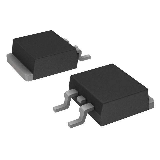
| 供应商器件封装 | TO-263(D2Pak) |
| 其它名称 | SUM110N06-3M9H-E3CT |
| 典型关闭延迟时间 | 75 ns |
| 功率-最大值 | 3.75W |
| 包装 | 剪切带 (CT) |
| 商标 | Vishay / Siliconix |
| 安装类型 | 表面贴装 |
| 安装风格 | SMD/SMT |
| 封装 | Reel |
| 封装/外壳 | TO-263-3,D²Pak(2 引线+接片),TO-263AB |
| 封装/箱体 | D2PAK-2 |
| 工厂包装数量 | 800 |
| 晶体管极性 | N-Channel |
| 最大工作温度 | + 175 C |
| 最小工作温度 | - 55 C |
| 标准包装 | 1 |
| 漏源极电压(Vdss) | 60V |
| 电流-连续漏极(Id)(25°C时) | 110A (Tc) |
| 系列 | SUM |
| 通道模式 | Enhancement |
| 配置 | Single |


- 商务部:美国ITC正式对集成电路等产品启动337调查
- 曝三星4nm工艺存在良率问题 高通将骁龙8 Gen1或转产台积电
- 太阳诱电将投资9.5亿元在常州建新厂生产MLCC 预计2023年完工
- 英特尔发布欧洲新工厂建设计划 深化IDM 2.0 战略
- 台积电先进制程称霸业界 有大客户加持明年业绩稳了
- 达到5530亿美元!SIA预计今年全球半导体销售额将创下新高
- 英特尔拟将自动驾驶子公司Mobileye上市 估值或超500亿美元
- 三星加码芯片和SET,合并消费电子和移动部门,撤换高东真等 CEO
- 三星电子宣布重大人事变动 还合并消费电子和移动部门
- 海关总署:前11个月进口集成电路产品价值2.52万亿元 增长14.8%


PDF Datasheet 数据手册内容提取
SUM110N06-3m9H Vishay Siliconix N-Channel 60-V (D-S) 175 °C MOSFET FEATURES PRODUCT SUMMARY • TrenchFET® Power MOSFET V (V) r (Ω) I (A) Q (Typ) (BR)DSS DS(on) D g 60 0.0039 at VGS = 10 V 110a 200 (cid:129) 175 °C Junction Temperature RoHS (cid:129) Low Thermal Resistance Package COMPLIANT (cid:129) High Threshold Voltage At High Temperature (cid:129) 100 % R Tested g D TO-263 G G D S Top View S Ordering Information:SUM110N06-3m9H-E3 (Lead (Pb)-free) N-Channel MOSFET ABSOLUTE MAXIMUM RATINGS T = 25°C, unless otherwise noted C Parameter Symbol Limit Unit Drain-Source Voltage VDS 60 V Gate-Source Voltage VGS ± 20 TC = 25 °C 110a Continuous Drain Current (TJ = 175 °C) TC = 125 °C ID 110a A Pulsed Drain Current IDM 440 Single Pulse Avalanche Current IAS 70 Single Pulse Avalanche Energy L = 0.1 mH EAS 245 mJ TC = 25 °C 375c Maximum Power Dissipationb T = 25 °Cd PD 3.75 W A Operating Junction and Storage Temperature Range TJ, Tstg - 55 to 175 °C THERMAL RESISTANCE RATINGS Parameter Symbol Limit Unit Junction-to-Ambient PCB Mountd RthJA 40 °C/W Junction-to-Case (Drain) RthJC 0.4 Notes: a. Package limited. b. Duty cycle ≤ 1 %. c. See SOA curve for voltage derating. d. When mounted on 1" square PCB (FR-4 material). Document Number: 73236 www.vishay.com S-70534-Rev. C, 26-Mar-07 1
SUM110N06-3m9H Vishay Siliconix SPECIFICATIONS T = 25°C, unless otherwise noted J Parameter Symbol Test Conditions Min Typ Max Unit Static Drain-Source Breakdown Voltage V(BR)DSS VGS = 0 V, ID = 250 µA 60 V Gate-Threshold Voltage VGS(th) VDS = VGS, ID = 250 µA 3.4 4.5 Gate-Body Leakage IGSS VDS = 0 V, VGS = ± 20 V 100 nA VDS = 60 V, VGS = 0 V 1 Zero Gate Voltage Drain Current IDSS VDS = 60 V, VGS = 0 V, TJ = 125 °C 50 µA VDS = 60 V, VGS = 0 V, TJ = 175 °C 250 On-State Drain Currenta ID(on) VDS ≥ 5 V, VGS = 10 V 120 A VGS = 10 V, ID = 30 A 0.00325 0.0039 Drain-Source On-State Resistancea rDS(on) VGS = 10 V, ID = 30 A, TJ = 125 °C 0.0063 Ω VGS = 10 V, ID = 30 A, TJ = 175 °C 0.0082 Forward Transconductancea gfs VDS = 15 V, ID = 30 A 30 S Dynamicb Input Capacitance Ciss 15 800 Output Capacitance Coss VGS = 0 V, VDS = 25 V, f = 1 MHz 1050 pF Reverse Transfer Capacitance Crss 600 Gate Resistance Rg f = 1 MHz 0.6 1.2 1.8 Ω Total Gate Chargec Qg 200 300 Gate-Source Chargec Qgs VDS = 30 V, VGS = 10 V, ID = 110 A 80 nC Gate-Drain Chargec Qgd 45 Turn-On Delay Timec td(on) 45 70 Rise Timec tr VDD = 30 V, RL = 0.27 Ω 160 240 ns Turn-Off Delay Timec td(off) ID ≅ 110 A, VGEN = 10 V, Rg = 2.5 Ω 75 115 Fall Timec tf 14 25 Source-Drain Diode Ratings and Characteristics (T = 25°C)b C Continuous Current IS 110 A Pulsed Current ISM 240 Forward Voltagea VSD IF = 85 A, VGS = 0 V 1.1 1.5 V Reverse Recovery Time trr 65 100 ns Peak Reverse Recovery Current IRM(REC) IF = 85 A, di/dt = 100 A/µs 4.4 6.6 A Reverse Recovery Charge Qrr 143 330 nC Notes: a. Pulse test; pulse width ≤ 300 µs, duty cycle ≤ 2 %. b. Guaranteed by design, not subject to production testing. c. Independent of operating temperature. Stresses beyond those listed under “Absolute Maximum Ratings” may cause permanent damage to the device. These are stress ratings only, and functional operation of the device at these or any other conditions beyond those indicated in the operational sections of the specifications is not implied. Exposure to absolute maximum rating conditions for extended periods may affect device reliability. www.vishay.com Document Number: 73236 2 S-70534-Rev. C, 26-Mar-07
SUM110N06-3m9H Vishay Siliconix TYPICAL CHARACTERISTICS 25°C, unless otherwise noted 250 250 VGS = 10 thru 7 V 200 200 Current (A) 150 6 V Current (A) 150 Drain 100 Drain 100 - ID - D TC = 125 °C I 50 50 25 °C 5 V -55 °C 0 0 0 2 4 6 8 10 0 1 2 3 4 5 6 7 VDS- Drain-to-Source Voltage (V) VGS- Gate-to-Source Voltage (V) Output Characteristics Transfer Characteristics 300 0.006 TC = -55 °C 250 25 °C 0.005 S) Ω) uctance ( 200 125 °C sistance ( 0.004 VGS = 10 V nd 150 Re 0.003 co n- s O an - Tr 100 n) 0.002 - fs DS(o g r 50 0.001 0 0.000 0 15 30 45 60 75 90 0 20 40 60 80 100 120 ID- Drain Current (A) ID- Drain Current (A) Transconductance On-Resistance vs. Drain Current 21000 20 18000 Ciss e (V) 16 VIDD =S 1=1 300 A V ance (pF) 1125000000 urce Voltag 12 cit So pa 9000 o- Ca e-t 8 C- 6000 - Gat Coss GS 4 3000 Crss V 0 0 0 10 20 30 40 50 60 0 50 100 150 200 250 300 350 400 VDS- Drain-to-Source Voltage (V) Qg- Total Gate Charge (nC) Capacitance Gate Charge Document Number: 73236 www.vishay.com S-70534-Rev. C, 26-Mar-07 3
SUM110N06-3m9H Vishay Siliconix TYPICAL CHARACTERISTICS 25°C, unless otherwise noted 2.0 100 VGS= 10 V ID = 30 A 1.7 ce A) On-Resistanmalized) 1.4 ce Current ( 10 TJ= 150 °C TJ= 25 °C - S(on)(Nor 1.1 - Sour D S r I 0.8 0.5 1 -50 -25 0 25 50 75 100 125 150 175 0 0.3 0.6 0.9 1.2 TJ- Junction Temperature (°C) VSD- Source-to-Drain Voltage (V) On-Resistance vs. Junction Temperature Source-Drain Diode Forward Voltage 1000 74 72 100 ID = 10 mA 70 IAV (A) at TA= 25 °C V) (a)Dav 10 (R)DSS 68 I V(B 66 IAV (A) at TA= 150 °C 64 1 62 0.1 60 -50 -25 0 25 50 75 100 125 150 175 0.00001 0.0001 0.001 0.01 0.1 1 tin (Sec) TJ- Junction Temperature (°C) Avalanche Current vs. Time Drain Source Breakdown vs. Junction Temperature www.vishay.com Document Number: 73236 4 S-70534-Rev. C, 26-Mar-07
SUM110N06-3m9H Vishay Siliconix THERMAL RATINGS 300 1000 10 µs 250 *Limited by rDS(on) 100 A) 200 A) 100 µs Current ( 150 Current ( 10 1 ms Drain Drain 1d0c, m10s0 ms - D 100 - D I Limited By Package I 1 TC = 25 °C 50 Single Pulse 0 0.1 0 25 50 75 100 125 150 175 0.1 1 10 100 TC- Case Temperature (°C) VDS- Drain-to-Source Voltage (V) *VGS minimum VGS at which rDS(on)isspecified Maximum Avalanche and Drain Current Safe Operating Area vs. Case Temperature 2 1 Duty Cycle = 0.5 nt e e Transiedance 0.2 ctivmp zed Effehermal I 0.1 0.002.050.1 maliT Single Pulse or N 0.01 10-4 10-3 10-2 10-1 1 Square Wave Pulse Duration (sec) Normalized Thermal Transient Impedance, Junction-to-Case Vishay Siliconix maintains worldwide manufacturing capability. Products may be manufactured at one of several qualified locations. Reliability data for Silicon Tech- nology and Package Reliability represent a composite of all qualified locations. For related documents such as package/tape drawings, part marking, and reliability data, see http://www.vishay.com/ppg?73236. Document Number: 73236 www.vishay.com S-70534-Rev. C, 26-Mar-07 5
Legal Disclaimer Notice Vishay Disclaimer All product specifications and data are subject to change without notice. Vishay Intertechnology, Inc., its affiliates, agents, and employees, and all persons acting on its or their behalf (collectively, “Vishay”), disclaim any and all liability for any errors, inaccuracies or incompleteness contained herein or in any other disclosure relating to any product. Vishay disclaims any and all liability arising out of the use or application of any product described herein or of any information provided herein to the maximum extent permitted by law. The product specifications do not expand or otherwise modify Vishay’s terms and conditions of purchase, including but not limited to the warranty expressed therein, which apply to these products. No license, express or implied, by estoppel or otherwise, to any intellectual property rights is granted by this document or by any conduct of Vishay. The products shown herein are not designed for use in medical, life-saving, or life-sustaining applications unless otherwise expressly indicated. Customers using or selling Vishay products not expressly indicated for use in such applications do so entirely at their own risk and agree to fully indemnify Vishay for any damages arising or resulting from such use or sale. Please contact authorized Vishay personnel to obtain written terms and conditions regarding products designed for such applications. Product names and markings noted herein may be trademarks of their respective owners. Document Number: 91000 www.vishay.com Revision: 18-Jul-08 1