ICGOO在线商城 > 分立半导体产品 > 晶体管 - FET,MOSFET - 单 > STY145N65M5
 Datasheet下载
- 型号: STY145N65M5
- 制造商: STMicroelectronics
- 库位|库存: xxxx|xxxx
- 要求:
| 数量阶梯 | 香港交货 | 国内含税 |
| +xxxx | $xxxx | ¥xxxx |
查看当月历史价格
查看今年历史价格
STY145N65M5产品简介:
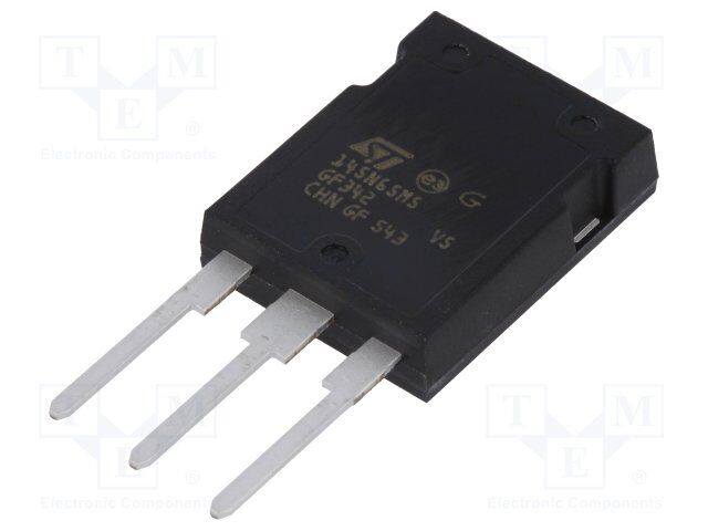
ICGOO电子元器件商城为您提供STY145N65M5由STMicroelectronics设计生产,在icgoo商城现货销售,并且可以通过原厂、代理商等渠道进行代购。 STY145N65M5价格参考¥177.92-¥183.39。STMicroelectronicsSTY145N65M5封装/规格:晶体管 - FET,MOSFET - 单, N-Channel 650V 138A (Tc) 625W (Tc) Through Hole MAX247™。您可以下载STY145N65M5参考资料、Datasheet数据手册功能说明书,资料中有STY145N65M5 详细功能的应用电路图电压和使用方法及教程。
| 参数 | 数值 |
| 产品目录 | |
| 描述 | MOSFET N-CH 650V 138A MAX247MOSFET N-Ch 650 V 0.012 Ohm 138 A MDmesh V |
| 产品分类 | FET - 单分离式半导体 |
| FET功能 | 标准 |
| FET类型 | MOSFET N 通道,金属氧化物 |
| Id-ContinuousDrainCurrent | 138 A |
| Id-连续漏极电流 | 138 A |
| 品牌 | STMicroelectronics |
| 产品手册 | |
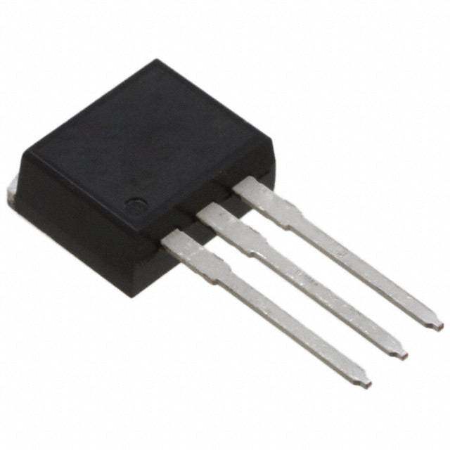
| 产品图片 |
|
| rohs | 符合RoHS无铅 / 符合限制有害物质指令(RoHS)规范要求 |
| 产品系列 | 晶体管,MOSFET,STMicroelectronics STY145N65M5MDmesh™ V |
| 数据手册 | |
| 产品型号 | STY145N65M5 |
| Pd-PowerDissipation | 625 W |
| Pd-功率耗散 | 625 W |
| Qg-GateCharge | 414 nC |
| Qg-栅极电荷 | 414 nC |
| RdsOn-Drain-SourceResistance | 15 mOhms |
| RdsOn-漏源导通电阻 | 15 mOhms |
| Vds-Drain-SourceBreakdownVoltage | 710 V |
| Vds-漏源极击穿电压 | 710 V |
| Vgs-Gate-SourceBreakdownVoltage | 25 V |
| Vgs-栅源极击穿电压 | 25 V |
| Vgsth-Gate-SourceThresholdVoltage | 4 V |
| Vgsth-栅源极阈值电压 | 4 V |
| 上升时间 | 11 ns |
| 下降时间 | 82 ns |
| 不同Id时的Vgs(th)(最大值) | 5V @ 250µA |
| 不同Vds时的输入电容(Ciss) | 18500pF @ 100V |
| 不同Vgs时的栅极电荷(Qg) | 414nC @ 10V |
| 不同 Id、Vgs时的 RdsOn(最大值) | 15 毫欧 @ 69A, 10V |
| 产品种类 | MOSFET |
| 供应商器件封装 | MAX-247 |
| 其它名称 | 497-13638-5 |
| 其它有关文件 | http://www.st.com/web/catalog/sense_power/FM100/CL824/SC1167/PF253737?referrer=70071840 |
| 功率-最大值 | 625W |
| 包装 | 管件 |
| 商标 | STMicroelectronics |
| 安装类型 | 通孔 |
| 安装风格 | Through Hole |
| 封装 | Tube |
| 封装/外壳 | MAX247™ |
| 封装/箱体 | Max247-3 |
| 工厂包装数量 | 30 |
| 晶体管极性 | N-Channel |
| 最大工作温度 | + 150 C |
| 最小工作温度 | - 55 C |
| 标准包装 | 30 |
| 漏源极电压(Vdss) | 650V |
| 特色产品 | http://www.digikey.cn/product-highlights/zh/mdmesh-v-power-mosfets/50075 |
| 电流-连续漏极(Id)(25°C时) | 138A (Tc) |
| 系列 | STY145N65M5 |
| 配置 | Single |


PDF Datasheet 数据手册内容提取
STY145N65M5 N-channel 650 V, 0.012 Ω typ., 138 A MDmesh™ M5 Power MOSFET in a Max247 package Datasheet - production data Features Order code VDS @ TJmax RDS(on) max. ID STY145N65M5 710 V 0.015 Ω 138 A • Extremely low R DS(on) • Low gate charge and input capacitance • Excellent switching performance 3 • 100% avalanche tested 2 1 Applications Max247 • Switching applications Figure 1: Internal schematic diagram Description This device is an N-channel Power MOSFET based on the MDmesh™ M5 innovative vertical process technology combined with the well- known PowerMESH™ horizontal layout. The resulting product offers extremely low on- resistance, making it particularly suitable for applications requiring high power and superior efficiency. Table 1: Device summary Order code Marking Package Packaging STY145N65M5 145N65M5 Max247 Tube November 2015 DocID023718 Rev 3 1/12 This is information on a product in full production. www.st.com
Contents STY145N65M5 Contents 1 Electrical ratings ............................................................................. 3 2 Electrical characteristics ................................................................ 4 2.1 Electrical characteristics (curves) ...................................................... 6 3 Test circuits ..................................................................................... 8 4 Package information ....................................................................... 9 4.1 Max247 package information ............................................................ 9 5 Revision history ............................................................................ 11 2/12 DocID023718 Rev 3
STY145N65M5 Electrical ratings 1 Electrical ratings Table 2: Absolute maximum ratings Symbol Parameter Value Unit VGS Gate-source voltage ± 25 V ID Drain current (continuous) at TC = 25 °C 138 A ID Drain current (continuous) at TC = 100 °C 87 A IDM(1) Drain current (pulsed) 552 A PTOT Total dissipation at TC = 25 °C 625 W Avalanche current, repetitive or not repetitive (pulse width IAR limited by Tjmax) 12 A EAS VSDinDg =le 5 p0u Vls)e avalanche energy (starting Tj = 25 °C, ID = IAR, 2420 mJ dv/dt(2) Peak diode recovery voltage slope 15 V/ns Tstg Storage temperature - 55 to 150 °C Tj Max. operating junction temperature 150 Notes: (1)Pulse width limited by safe operating area. (2)ISD ≤ 138 A, di/dt ≤ 400 A/µs; VDS(peak) < V(BR)DSS, VDD = 400 V. Table 3: Thermal data Symbol Parameter Value Unit Rthj-case Thermal resistance junction-case max 0.2 °C/W Rthj-amb Thermal resistance junction-ambient max 30 °C/W DocID023718 Rev 3 3/12
Electrical characteristics STY145N65M5 2 Electrical characteristics T = 25 °C unless otherwise specified C Table 4: On/off states Symbol Parameter Test conditions Min. Typ. Max. Unit Drain-source breakdown V(BR)DSS voltage VGS = 0 V, ID = 1 mA 650 V VGS = 0 V, VDS = 650 V 10 µA Zero gate voltage drain IDSS current VGS = 0 V, VDS = 650 V, 100 µA TC = 125 °C IGSS Gate-body leakage current VDS = 0 V, VGS = ±25 V ±100 nA VGS(th) Gate threshold voltage VDS = VGS, ID = 250 µA 3 4 5 V Static drain-source RDS(on) on-resistance VGS = 10 V, ID = 69 A 0.012 0.015 Ω Table 5: Dynamic Symbol Parameter Test conditions Min. Typ. Max. Unit Ciss Input capacitance - 18500 - pF Coss Output capacitance VDS= 100 V, f = 1 MHz, - 413 - pF Reverse transfer VGS = 0 V Crss capacitance - 11 - pF Equivalent output Co(er)(1) capacitance energy - 415 - pF related VGS = 0, VDS = 0 to 520 V Co(tr)(2) Ecaqpuaivcaitlaennct eo utitmpuet related - 1950 - pF RG Intrinsic gate resistance f = 1 MHz, open drain - 0.7 - Ω Qg Total gate charge VDD = 520 V, ID = 69 A, - 414 - nC Qgs Gate-source charge V"TGeSs =t c1ir0c uVi t( sfoere g Faitgeu creh a1r5g:e - 114 - nC Qgd Gate-drain charge behavior") - 164 - nC Notes: (1) Co(er) is defined as a constant equivalent capacitance giving the same stored energy as Coss when VDS increases from 0 to 80% VDSS (2) Co(tr) is defined as a constant equivalent capacitance giving the same charging time as Coss when VDS increases from 0 to 80% VDSS 4/12 DocID023718 Rev 3
STY145N65M5 Electrical characteristics Table 6: Switching times Symbol Parameter Test conditions Min. Typ. Max. Unit td(V) Voltage delay time VDD = 400 V, ID = 85 A - 255 - ns tr(V) Voltage rise time RG = 4.7 Ω, VGS = 10 V - 11 - ns (see Figure 16: "Test circuit tf(i) Current fall time for inductive load switching - 82 - ns and diode recovery times" tC(off) Crossing time and Figure 19: "Switching - 88 - ns time waveform") Table 7: Source drain diode Symbol Parameter Test conditions Min. Typ. Max. Unit ISD Source-drain current - 138 A ISDM,(1) Source-drain current (pulsed) - 552 A VSD (2) Forward on voltage VGS = 0 V, ISD = 138 A - 1.5 V trr Reverse recovery time ISD = 138 A, - 568 ns di/dt = 100 A/µs, Qrr Reverse recovery charge VDD = 100 V (see Figure - 14.5 µC 16: "Test circuit for IRRM Reverse recovery current inductive load switching - 51 A and diode recovery times") trr Reverse recovery time ISD = 138 A, - 728 ns di/dt = 100 A/µs, Qrr Reverse recovery charge VDD = 100 V, Tj = 150 °C - 24.5 µC (see Figure 16: "Test circuit IRRM Reverse recovery current for inductive load switching - 67 A and diode recovery times") Notes: (1)Pulse width is limited by safe operating area (2)Pulsed: pulse duration = 300 µs, duty cycle 1.5% DocID023718 Rev 3 5/12
Electrical characteristics STY145N65M5 2.2 Electrical characteristics (curves) Figure 2: Safe operating area Figure 3: Thermal impedance AM09125v1 K δ=0.5 0.2 0.1 0.05 10-1 0.02 0.01 Zth=kRthj-c d=tp/t Single pulse tp t 10-2 10-4 10-3 10-2 10-1 tp(s) Figure 4: Output characteristics Figure 5: Transfer characteristics AM17901v1 AM17902v1 ID(A) ID VGS=10V 9V (A) VDS=30V 300 300 8V 250 250 200 200 150 150 7V 100 100 50 50 6V 0 0 0 5 10 15 20 25 VDS(V) 0 1 2 3 4 5 6 7 8 VGS(V) Figure 6: Gate charge vs gate-source voltage Figure 7: Static drain-source on-resistance 6/12 DocID023718 Rev 3
STY145N65M5 Electrical characteristics Figure 8: Capacitance variations Figure 9: Normalized gate threshold voltage vs temperature C AM15553v1 VGS(th) AM08899v1 (pF) (norm) 1.10 100000 ID= 250µA VDS=VGS Ciss 10000 1.00 1000 0.90 Coss 100 f=1 MHz 0.80 10 Crss 1 0.70 0.1 1 10 100 VDS(V) -50 -25 0 25 50 75 100 TJ(°C) Figure 10: Normalized on-resistance vs Figure 11: Normalized V(BR)DSS vs temperature temperature RDS(on) AM08900v1 V(BR)DSS AM10399v1 (norm) (norm) 2.1 1.08 ID = 69A 1.06 ID = 1mA VGS= 10V 1.7 1.04 1.02 1.3 1.00 0.98 0.9 0.96 0.94 0.5 0.92 -50 -25 0 25 50 75 100 TJ(°C) -50 -25 0 25 50 75 100 TJ(°C) Figure 12: Output capacitance stored energy Figure 13: Switching losses vs gate resistance AM15555v1 E(µJ) 9000 VDD=400V Eon VGS=10V 8000 ID=85 A 7000 6000 5000 4000 Eoff 3000 2000 1000 0 0 10 20 30 40 RG(W) The previous figure E includes reverse recovery of a SiC diode. on DocID023718 Rev 3 7/12
Test circuits STY145N65M5 3 Test circuits Figure 14: Test circuit for resistive load Figure 15: Test circuit for gate charge switching times behavior Figure 16: Test circuit for inductive load Figure 17: Unclamped inductive load test switching and diode recovery times circuit Figure 18: Unclamped inductive waveform Figure 19: Switching time waveform ConceptwaveformforInductiveLoadTurn-off Id 90%Vds 90%Id Tdelay--ooffff Vgs 90%Vgs oonn Vgs(I(t)))) 10%Vds 10%Id Vds TTrriissee TTffaallll Tcross--over AM05540v2_for_M5 8/12 DocID023718 Rev 3
STY145N65M5 Package information 4 Package information In order to meet environmental requirements, ST offers these devices in different grades of ECOPACK® packages, depending on their level of environmental compliance. ECOPACK® specifications, grade definitions and product status are available at: www.st.com. ECOPACK® is an ST trademark. 4.1 Max247 package information Figure 20: Max247 package outline 0094330_Rev_D DocID023718 Rev 3 9/12
Package information STY145N65M5 Table 8: Max247 package mechanical data mm Dim. Min. Typ. Max. A 4.70 - 5.30 A1 2.20 - 2.60 b 1.00 - 1.40 b1 2.00 - 2.40 b2 3.00 - 3.40 c 0.40 - 0.80 D 19.70 - 20.30 e 5.35 - 5.55 E 15.30 - 15.90 L 14.20 - 15.20 L1 3.70 - 4.30 10/12 DocID023718 Rev 3
STY145N65M5 Revision history 5 Revision history Table 9: Document revision history Date Revision Changes 25-Sep-2012 1 First release. Modified: IAR and EAS values 17-Jan-2013 2 Modified: typical values on Table 5, 6 and 7 Updated title, features and description on cover page. Document status promoted from preliminary to production data. Modified: Table 2: "Absolute maximum ratings" and Table 3: "Thermal 13-Nov-2015 3 data" Updated: Figure 4: "Output characteristics" and Figure 5: "Transfer characteristics" Minor text changes. DocID023718 Rev 3 11/12
STY145N65M5 IMPORTANT NOTICE – PLEASE READ CAREFULLY STMicroelectronics NV and its subsidiaries (“ST”) reserve the right to make changes, corrections, enhancements, modifications, and improvements to ST products and/or to this document at any time without notice. Purchasers should obtain the latest relevant information on ST products before placing orders. ST products are sold pursuant to ST’s terms and conditions of sale in place at the time of order acknowledgement. Purchasers are solely responsible for the choice, selection, and use of ST products and ST assumes no liability for application assistance or the design of Purchasers’ products. No license, express or implied, to any intellectual property right is granted by ST herein. Resale of ST products with provisions different from the information set forth herein shall void any warranty granted by ST for such product. ST and the ST logo are trademarks of ST. All other product or service names are the property of their respective owners. Information in this document supersedes and replaces information previously supplied in any prior versions of this document. © 2015 STMicroelectronics – All rights reserved 12/12 DocID023718 Rev 3
Mouser Electronics Authorized Distributor Click to View Pricing, Inventory, Delivery & Lifecycle Information: S TMicroelectronics: STY145N65M5