ICGOO在线商城 > 分立半导体产品 > 晶体管 - FET,MOSFET - 单 > STW9N150
 Datasheet下载
- 型号: STW9N150
- 制造商: STMicroelectronics
- 库位|库存: xxxx|xxxx
- 要求:
| 数量阶梯 | 香港交货 | 国内含税 |
| +xxxx | $xxxx | ¥xxxx |
查看当月历史价格
查看今年历史价格
STW9N150产品简介:
ICGOO电子元器件商城为您提供STW9N150由STMicroelectronics设计生产,在icgoo商城现货销售,并且可以通过原厂、代理商等渠道进行代购。 STW9N150价格参考。STMicroelectronicsSTW9N150封装/规格:晶体管 - FET,MOSFET - 单, 通孔 N 沟道 1500V 8A(Tc) 320W(Tc) TO-247-3。您可以下载STW9N150参考资料、Datasheet数据手册功能说明书,资料中有STW9N150 详细功能的应用电路图电压和使用方法及教程。
STMicroelectronics的STW9N150是一款单通道MOSFET(金属-氧化物-半导体场效应晶体管),主要用于高效能开关和功率管理应用。以下是其主要应用场景:

 1. 电源管理系统
STW9N150适用于各种电源转换和调节电路,如开关模式电源(SMPS)、直流-直流(DC-DC)转换器等。它能够实现高效的电压转换,减少能量损耗,提高电源系统的整体效率。特别适用于需要高电流、低导通电阻的应用场景。

 2. 电机驱动
在电机控制领域,STW9N150可以用于驱动小型直流电机或步进电机。由于其低导通电阻特性,能够有效降低发热,提升电机驱动的效率和可靠性。此外,它还可以用于无刷直流电机(BLDC)的电子换向系统中,确保电机平稳运行。

 3. 电池管理系统
STW9N150可用于电池保护电路,作为充放电路径中的开关元件。它能够快速响应过流、短路等异常情况,保护电池免受损坏。同时,其低导通电阻有助于减少电池内部的能量损耗,延长电池寿命。

 4. 工业自动化
在工业自动化设备中,STW9N150常用于控制信号的传输和处理。例如,在PLC(可编程逻辑控制器)中,它可以作为输入/输出端口的开关元件,实现对传感器、执行器等外围设备的精准控制。此外,它还适用于工业机器人的关节驱动、伺服控制系统等场合。

 5. 消费电子产品
STW9N150广泛应用于各类消费电子产品中,如智能手机、平板电脑、笔记本电脑等。它可以在充电电路、背光驱动、音频放大器等模块中发挥重要作用,提供高效稳定的电力支持,同时保证产品的轻薄设计和长续航能力。

 6. 汽车电子
在汽车电子领域,STW9N150可用于车载充电器、电动助力转向系统(EPS)、车身电子控制单元(ECU)等关键部件。其出色的耐压和耐温性能,确保了在复杂多变的车载环境中稳定可靠的工作表现。

综上所述,STW9N150凭借其优异的电气特性和广泛的适用性,在多个领域中展现出卓越的性能,满足不同应用场景的需求。
| 参数 | 数值 |
| 产品目录 | |
| ChannelMode | Enhancement |
| 描述 | MOSFET N-CH 1500V 8A TO-247MOSFET N-CH 1500V HI-VOLT PWRMESH PWR MOSFET |
| 产品分类 | FET - 单分离式半导体 |
| FET功能 | 标准 |
| FET类型 | MOSFET N 通道,金属氧化物 |
| Id-ContinuousDrainCurrent | 8 A |
| 品牌 | STMicroelectronics |
| 产品手册 | |
| 产品图片 |
|
| rohs | 符合RoHS无铅 / 符合限制有害物质指令(RoHS)规范要求 |
| 产品系列 | 晶体管,MOSFET,STMicroelectronics STW9N150PowerMESH™ |
| 数据手册 | |
| 产品型号 | STW9N150 |
| Pd-PowerDissipation | 320 W |
| RdsOn-Drain-SourceResistance | 2.5 Ohms |
| Vds-Drain-SourceBreakdownVoltage | 1.5 kV |
| Vgs-Gate-SourceBreakdownVoltage | +/- 30 V |
| 上升时间 | 14.7 ns |
| 下降时间 | 52 ns |
| 不同Id时的Vgs(th)(最大值) | 5V @ 250µA |
| 不同Vds时的输入电容(Ciss) | 3255pF @ 25V |
| 不同Vgs时的栅极电荷(Qg) | 89.3nC @ 10V |
| 不同 Id、Vgs时的 RdsOn(最大值) | 2.5 欧姆 @ 4A,10V |
| 产品目录页面 | |
| 产品种类 | Power MOSFET Transistors |
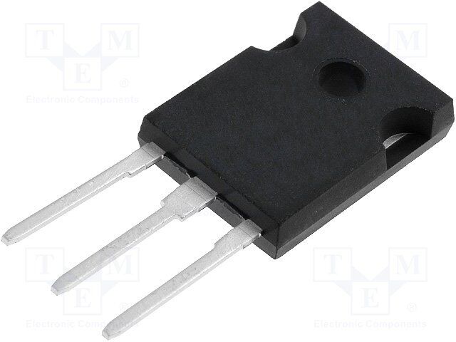
| 供应商器件封装 | TO-247-3 |
| 其它名称 | 497-8465-5 |
| 其它有关文件 | http://www.st.com/web/catalog/sense_power/FM100/CL824/SC1168/PF167035?referrer=70071840 |
| 典型关闭延迟时间 | 86 ns |
| 功率-最大值 | 320W |
| 包装 | 管件 |
| 参考设计库 | http://www.digikey.com/rdl/4294959904/4294959862/146 |
| 商标 | STMicroelectronics |
| 安装类型 | 通孔 |
| 安装风格 | Through Hole |
| 封装 | Tube |
| 封装/外壳 | TO-247-3 |
| 封装/箱体 | TO-247 |
| 工具箱 | /product-detail/zh/Q7096737/497-8014-KIT-ND/3479580 |
| 工厂包装数量 | 30 |
| 晶体管极性 | N-Channel |
| 最大工作温度 | + 150 C |
| 最小工作温度 | - 55 C |
| 标准包装 | 30 |
| 漏源极电压(Vdss) | 1500V(1.5kV) |
| 特色产品 | http://www.digikey.com/cn/zh/ph/ST/MOSFET.html |
| 电流-连续漏极(Id)(25°C时) | 8A (Tc) |
| 系列 | STW9N150 |
| 配置 | Single |


PDF Datasheet 数据手册内容提取
STW9N150 Ω N-channel 1500 V - 1.8 - 8 A - TO-247 very high voltage PowerMESH™ Power MOSFET Features Type V R I Pw DSS DS(on) D STW9N150 1500 V < 2.5 Ω 8 A 320 W ■ 100% avalanche tested ■ Avalanche ruggedness 3 ■ Gate charge minimized 2 1 ■ Very low intrinsic capacitances TO-247 ■ High speed switching ■ Very low on-resistance Application ■ Switching applications Figure 1. Internal schematic diagram Description Using the well consolidated high voltage MESH OVERLAY™ process, STMicroelectronics has designed an advanced family of Power MOSFETs with outstanding performances. The strengthened layout coupled with the company’s proprietary edge termination structure, gives the lowest R per area, unrivalled gate charge and DS(on) switching characteristics. Table 1. Device summary Order code Marking Package Packaging STW9N150 9N150 TO-247 Tube January 2008 Rev 2 1/12 www.st.com 12
Contents STW9N150 Contents 1 Electrical ratings . . . . . . . . . . . . . . . . . . . . . . . . . . . . . . . . . . . . . . . . . . . . 3 2 Electrical characteristics . . . . . . . . . . . . . . . . . . . . . . . . . . . . . . . . . . . . . 4 2.1 Electrical characteristics (curves) . . . . . . . . . . . . . . . . . . . . . . . . . . . . . 5 3 Test circuits . . . . . . . . . . . . . . . . . . . . . . . . . . . . . . . . . . . . . . . . . . . . . . 8 4 Package mechanical data . . . . . . . . . . . . . . . . . . . . . . . . . . . . . . . . . . . . . 9 5 Revision history . . . . . . . . . . . . . . . . . . . . . . . . . . . . . . . . . . . . . . . . . . . 11 2/12
STW9N150 Electrical ratings 1 Electrical ratings Table 2. Absolute maximum ratings Symbol Parameter Value Unit V Drain-source voltage (V = 0) 1500 V DS GS V Gate- source voltage ± 30 V GS I Drain current (continuous) at T = 25 °C 8 A D C I Drain current (continuous) at T = 100 °C 5 A D C I (1) Drain current (pulsed) 32 A DM P Total dissipation at T = 25 °C 320 W TOT C Derating factor 2.56 W/°C T Operating junction temperature J -55 to 150 °C T Storage temperature stg 1. Pulse width limited by safe operating area Table 3. Thermal data Symbol Parameter Value Unit Rthj-case Thermal resistance junction-case max 0.39 °C/W Rthj-amb Thermal resistance junction-ambient max 50 °C/W T Maximum lead temperature for soldering purpose 300 °C/W J Table 4. Avalanche characteristics Symbol Parameter Max value Unit Avalanche current, repetitive or not-repetitive I 8 A AR (pulse width limited by T max) J Single pulse avalanche energy E 720 mJ AS (starting T = 25 °C, I = I , V = 50 V) J D AR DD 3/12
Electrical characteristics STW9N150 2 Electrical characteristics (Tcase =25°C unless otherwise specified) Table 5. On /off states Symbol Parameter Test conditions Min. Typ. Max. Unit Drain-source V I = 1 mA, V = 0 1500 V (BR)DSS breakdown voltage D GS Zero gate voltage V = Max rating 10 µA I DS DSS drain current (V = 0) V = Max rating, T =125 °C 500 µA GS DS C Gate-body leakage I V = ± 30 V ± 100 nA GSS current (V = 0) GS DS V Gate threshold voltage V = V , I = 250 µA 3 4 5 V GS(th) DS GS D Static drain-source on R V = 10 V, I = 4 A 1.8 2.5 Ω DS(on resistance GS D Table 6. Dynamic Symbol Parameter Test conditions Min. Typ. Max. Unit Forward g (1) V = 15 V, I = 4 A 7.5 S fs transconductance DS D Input capacitance C 3255 pF iss Output capacitance C V = 25 V, f = 1 MHz, V = 0 294 pF oss DS GS Reverse transfer C 22.4 pF rss capacitance Equivalent Output C V = 0, V = 0 to 1200 V 118 pF oss eq. capacitance GS DS f=1MHz Gate DC Bias=0 R Gate input resistance Test signal level=20 mV 2.4 Ω g open drain Q Total gate charge V = 1200 V, I = 8 A, 89.3 nC g DD D Q Gate-source charge V = 10 V 15.8 nC gs GS Q Gate-drain charge (see Figure 15) 50.4 nC gd 1. Pulsed: Pulse duration = 300 µs, duty cycle 1.5% 4/12
STW9N150 Electrical characteristics Table 7. Switching times Symbol Parameter Test conditions Min. Typ. Max Unit t Turn-on delay time 41 ns d(on) V = 750 V, I = 4 A, t Rise time DD D 14.7 ns r R = 4.7 Ω, V = 10 V t Turn-off-delay time G GS 86 ns d(off) (see Figure 14) t Fall time 52 ns f Table 8. Source drain diode Symbol Parameter Test conditions Min. Typ. Max Unit I Source-drain current 8 A SD I (1) Source-drain current (pulsed) 32 A SDM V (2) Forward on voltage I = 8 A, V = 0 1.6 V SD SD GS t Reverse recovery time I = 8 A, di/dt = 100 A/µs 988 ns rr SD Q Reverse recovery charge V = 60 V 9.5 µC rr DD I Reverse recovery current (see Figure 16) 19.3 A RRM t Reverse recovery time I = 8 A, di/dt = 100 A/µs 884 ns rr SD Q Reverse recovery charge V = 60 V T = 150 °C 8.2 µC rr DD J I Reverse recovery current (see Figure 16) 18.6 A RRM 1. Pulse width limited by safe operating area 2. Pulsed: pulse duration = 300 µs, duty cycle 1.5% 5/12
Electrical characteristics STW9N150 2.1 Electrical characteristics (curves) Figure 2. Safe operating area Figure 3. Thermal impedance Figure 4. Output characteristics Figure 5. Transfer characteristics Figure 6. Normalized BV vs temperature Figure 7. Static drain-source on resistance DSS RDS(on) HV41520 (Ω) 1.9 VGS =10V 1.8 1.7 1.6 1.5 0 1 2 3 4 5 6 ID(A) 6/12
STW9N150 Electrical characteristics Figure 8. Gate charge vs gate-source voltage Figure 9. Capacitance variations HV41500 V(VGS) VDDID = =182A00V VGS =10V 10 8 6 4 2 0 0 20 40 60 80 100 Qg (nC) Figure 10. Normalized gate threshold voltage Figure 11. Normalized on resistance vs vs temperature temperature Figure 12. Source-drain diode forward Figure 13. Maximum avalanche energy vs characteristics temperature HV41480 EAS (mJ) 700 ID = 8A 600 500 400 300 200 100 0 0 25 50 75 100 125 TJ (˚C) 7/12
Test circuits STW9N150 3 Test circuits Figure 14. Switching times test circuit for Figure 15. Gate charge test circuit resistive load Figure 16. Test circuit for inductive load Figure 17. Unclamped Inductive load test switching and diode recovery times circuit Figure 18. Unclamped inductive waveform Figure 19. Switching time waveform 8/12
STW9N150 Package mechanical data 4 Package mechanical data In order to meet environmental requirements, ST offers these devices in ECOPACK® packages. These packages have a Lead-free second level interconnect. The category of second level interconnect is marked on the package and on the inner box label, in compliance with JEDEC Standard JESD97. The maximum ratings related to soldering conditions are also marked on the inner box label. ECOPACK is an ST trademark. ECOPACK specifications are available at: www.st.com 9/12
Package mechanical data STW9N150 TO-247 MECHANICAL DATA mm. inch DIM. MIN. TYP MAX. MIN. TYP. MAX. A 4.85 5.15 0.19 0.20 A1 2.20 2.60 0.086 0.102 b 1.0 1.40 0.039 0.055 b1 2.0 2.40 0.079 0.094 b2 3.0 3.40 0.118 0.134 c 0.40 0.80 0.015 0.03 D 19.85 20.15 0.781 0.793 E 15.45 15.75 0.608 0.620 e 5.45 0.214 L 14.20 14.80 0.560 0.582 L1 3.70 4.30 0.14 0.17 L2 18.50 0.728 øP 3.55 3.65 0.140 0.143 øR 4.50 5.50 0.177 0.216 S 5.50 0.216 10/12
STW9N150 Revision history 5 Revision history T able 9. Document revision history Date Revision Changes 24-May-2007 1 First release 04-Jan-2007 2 Document status promoted from preliminary data to datasheet 11/12
STW9N150 Please Read Carefully: Information in this document is provided solely in connection with ST products. STMicroelectronics NV and its subsidiaries (“ST”) reserve the right to make changes, corrections, modifications or improvements, to this document, and the products and services described herein at any time, without notice. All ST products are sold pursuant to ST’s terms and conditions of sale. Purchasers are solely responsible for the choice, selection and use of the ST products and services described herein, and ST assumes no liability whatsoever relating to the choice, selection or use of the ST products and services described herein. No license, express or implied, by estoppel or otherwise, to any intellectual property rights is granted under this document. If any part of this document refers to any third party products or services it shall not be deemed a license grant by ST for the use of such third party products or services, or any intellectual property contained therein or considered as a warranty covering the use in any manner whatsoever of such third party products or services or any intellectual property contained therein. UNLESS OTHERWISE SET FORTH IN ST’S TERMS AND CONDITIONS OF SALE ST DISCLAIMS ANY EXPRESS OR IMPLIED WARRANTY WITH RESPECT TO THE USE AND/OR SALE OF ST PRODUCTS INCLUDING WITHOUT LIMITATION IMPLIED WARRANTIES OF MERCHANTABILITY, FITNESS FOR A PARTICULAR PURPOSE (AND THEIR EQUIVALENTS UNDER THE LAWS OF ANY JURISDICTION), OR INFRINGEMENT OF ANY PATENT, COPYRIGHT OR OTHER INTELLECTUAL PROPERTY RIGHT. UNLESS EXPRESSLY APPROVED IN WRITING BY AN AUTHORIZED ST REPRESENTATIVE, ST PRODUCTS ARE NOT RECOMMENDED, AUTHORIZED OR WARRANTED FOR USE IN MILITARY, AIR CRAFT, SPACE, LIFE SAVING, OR LIFE SUSTAINING APPLICATIONS, NOR IN PRODUCTS OR SYSTEMS WHERE FAILURE OR MALFUNCTION MAY RESULT IN PERSONAL INJURY, DEATH, OR SEVERE PROPERTY OR ENVIRONMENTAL DAMAGE. ST PRODUCTS WHICH ARE NOT SPECIFIED AS "AUTOMOTIVE GRADE" MAY ONLY BE USED IN AUTOMOTIVE APPLICATIONS AT USER’S OWN RISK. Resale of ST products with provisions different from the statements and/or technical features set forth in this document shall immediately void any warranty granted by ST for the ST product or service described herein and shall not create or extend in any manner whatsoever, any liability of ST. ST and the ST logo are trademarks or registered trademarks of ST in various countries. Information in this document supersedes and replaces all information previously supplied. The ST logo is a registered trademark of STMicroelectronics. All other names are the property of their respective owners. © 2008 STMicroelectronics - All rights reserved STMicroelectronics group of companies Australia - Belgium - Brazil - Canada - China - Czech Republic - Finland - France - Germany - Hong Kong - India - Israel - Italy - Japan - Malaysia - Malta - Morocco - Singapore - Spain - Sweden - Switzerland - United Kingdom - United States of America www.st.com 12/12
Mouser Electronics Authorized Distributor Click to View Pricing, Inventory, Delivery & Lifecycle Information: S TMicroelectronics: STW9N150