ICGOO在线商城 > 分立半导体产品 > 晶体管 - FET,MOSFET - 单 > STW7N95K3
 Datasheet下载
- 型号: STW7N95K3
- 制造商: STMicroelectronics
- 库位|库存: xxxx|xxxx
- 要求:
| 数量阶梯 | 香港交货 | 国内含税 |
| +xxxx | $xxxx | ¥xxxx |
查看当月历史价格
查看今年历史价格
STW7N95K3产品简介:
ICGOO电子元器件商城为您提供STW7N95K3由STMicroelectronics设计生产,在icgoo商城现货销售,并且可以通过原厂、代理商等渠道进行代购。 STW7N95K3价格参考¥询价-¥询价。STMicroelectronicsSTW7N95K3封装/规格:晶体管 - FET,MOSFET - 单, 通孔 N 沟道 950V 7.2A(Tc) 150W(Tc) TO-247-3。您可以下载STW7N95K3参考资料、Datasheet数据手册功能说明书,资料中有STW7N95K3 详细功能的应用电路图电压和使用方法及教程。
| 参数 | 数值 |
| 产品目录 | |
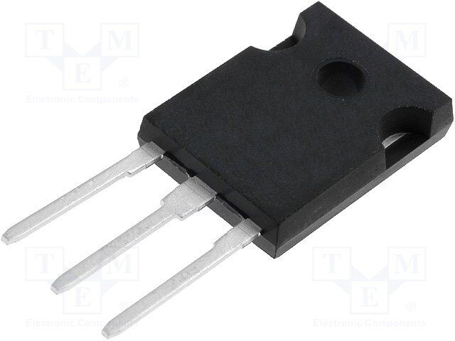
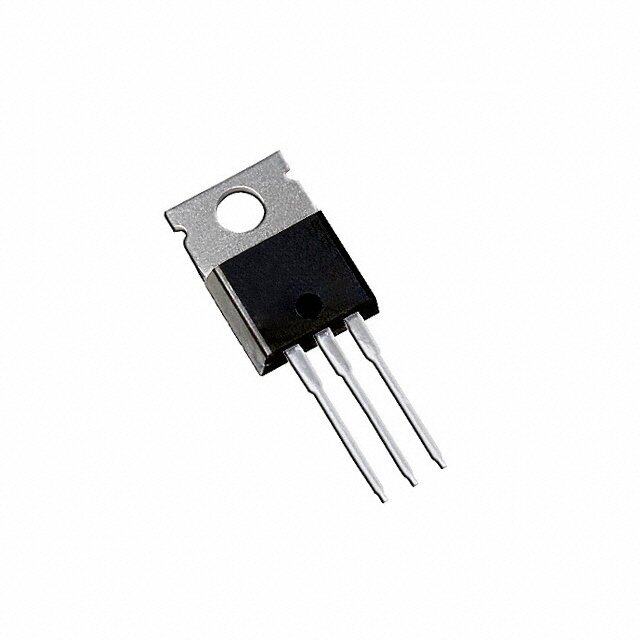
| 描述 | MOSFET N-CH 950V 7.2A TO-247 |
| 产品分类 | FET - 单 |
| FET功能 | 标准 |
| FET类型 | MOSFET N 通道,金属氧化物 |
| 品牌 | STMicroelectronics |
| 数据手册 | |
| 产品图片 |
|
| 产品型号 | STW7N95K3 |
| rohs | 无铅 / 符合限制有害物质指令(RoHS)规范要求 |
| 产品系列 | SuperMESH3™ |
| 不同Id时的Vgs(th)(最大值) | 5V @ 100µA |
| 不同Vds时的输入电容(Ciss) | 1031pF @ 100V |
| 不同Vgs时的栅极电荷(Qg) | 34nC @ 10V |
| 不同 Id、Vgs时的 RdsOn(最大值) | 1.35 欧姆 @ 3.6A,10V |
| 产品目录页面 | |
| 供应商器件封装 | TO-247-3 |
| 其它名称 | 497-8798-5 |
| 其它有关文件 | http://www.st.com/web/catalog/sense_power/FM100/CL824/SC1168/PF219921?referrer=70071840 |
| 功率-最大值 | 150W |
| 包装 | 管件 |
| 安装类型 | 通孔 |
| 封装/外壳 | TO-247-3 |
| 标准包装 | 30 |
| 漏源极电压(Vdss) | 950V |
| 电流-连续漏极(Id)(25°C时) | 7.2A (Tc) |


- 商务部:美国ITC正式对集成电路等产品启动337调查
- 曝三星4nm工艺存在良率问题 高通将骁龙8 Gen1或转产台积电
- 太阳诱电将投资9.5亿元在常州建新厂生产MLCC 预计2023年完工
- 英特尔发布欧洲新工厂建设计划 深化IDM 2.0 战略
- 台积电先进制程称霸业界 有大客户加持明年业绩稳了
- 达到5530亿美元!SIA预计今年全球半导体销售额将创下新高
- 英特尔拟将自动驾驶子公司Mobileye上市 估值或超500亿美元
- 三星加码芯片和SET,合并消费电子和移动部门,撤换高东真等 CEO
- 三星电子宣布重大人事变动 还合并消费电子和移动部门
- 海关总署:前11个月进口集成电路产品价值2.52万亿元 增长14.8%
.jpg)


PDF Datasheet 数据手册内容提取
STF7N95K3 STP7N95K3, STW7N95K3 N-channel 950 V, 1.1 Ω, 7.2 A, TO-220, TO-220FP, TO-247 Zener-protected SuperMESH3™ Power MOSFET Features R Type V DS(on) I Pw DSS max D STF7N95K3 950 V < 1.35 Ω 7.2 A 35 W 3 2 1 STP7N95K3 950 V < 1.35 Ω 7.2 A 150 W TO-247 STW7N95K3 950 V < 1.35 Ω 7.2 A 150 W ■ 100% avalanche tested 3 2 1 ■ Extremely large avalanche performance TO-220 3 ■ Gate charge minimized 2 1 ■ Very low intrinsic capacitances TO-220FP ■ Zener-protected Application Figure 1. Internal schematic diagram ■ Switching applications Description The new SuperMESH3™ series is obtained through the combination of a further fine tuning of ST's well established strip-based PowerMESH™ layout with a new optimized vertical structure. In addition to pushing on-resistance significantly down, special attention has been taken to ensure a very good dynamic performances coupled with a very large avalanche capability for the most demanding application. Table 1. Device summary Order codes Marking Package Packaging STF7N95K3 7N95K3 TO-220FP Tube STP7N95K3 7N95K3 TO-220 Tube STW7N95K3 7N95K3 TO-247 Tube January 2009 Rev 1 1/15 www.st.com 15
Contents STF7N95K3, STP7N95K3, STW7N95K3 Contents 1 Electrical ratings . . . . . . . . . . . . . . . . . . . . . . . . . . . . . . . . . . . . . . . . . . . . 3 2 Electrical characteristics . . . . . . . . . . . . . . . . . . . . . . . . . . . . . . . . . . . . . 4 2.1 Electrical characteristics (curves) . . . . . . . . . . . . . . . . . . . . . . . . . . . . 6 3 Test circuits . . . . . . . . . . . . . . . . . . . . . . . . . . . . . . . . . . . . . . . . . . . . . . 9 4 Package mechanical data . . . . . . . . . . . . . . . . . . . . . . . . . . . . . . . . . . . . 10 5 Revision history . . . . . . . . . . . . . . . . . . . . . . . . . . . . . . . . . . . . . . . . . . . 14 2/15
STF7N95K3, STP7N95K3, STW7N95K3 Electrical ratings 1 Electrical ratings Table 2. Absolute maximum ratings Value Symbol Parameter Unit TO-220, TO-247 TO-220FP V Gate-source voltage ± 30 V GS I Drain current (continuous) at T = 25 °C 7.2 7.2 (1) A D C I Drain current (continuous) at T = 100 °C 4.5 4.5 (1) A D C I (2) Drain current (pulsed) 28.8 28.8 (1) A DM P Total dissipation at T = 25 °C 150 35 W TOT C Max current during repetitive or single pulse I 9 A AR avalanche (pulse width limited by T ) JMAX E Single pulse avalanche energy (3) 220 mJ AS Derating factor 1.12 0.24 W/°C dv/dt (4) Peak diode recovery voltage slope 6 V/ns Insulation withstand voltage (RMS) from all three V leads to external heat sink 2000 V ISO (t=1 s;T =25 °C) C T Operating junction temperature j -55 to 150 °C T Storage temperature stg 1. Limited by package 2. Pulse width limited by safe operating area 3. Starting T = 25 °C, I = I , V = 50 V j D AR DD 4. I ≤ 7.2 A, di/dt = 100 A/µs, V < V SD Peak (BR)DSS Table 3. Thermal data Symbol Parameter TO-220 TO-247 TO-220FP Unit R Thermal resistance junction-case max 0.83 3.57 °C/W thj-case Rt Thermal resistance junction-ambient max 62.5 50 62.5 °C/W hj-amb T Maximum lead temperature for soldering purpose 300 °C l 3/15
Electrical characteristics STF7N95K3, STP7N95K3, STW7N95K3 2 Electrical characteristics (Tcase = 25 °C unless otherwise specified) Table 4. On /off states Symbol Parameter Test conditions Min. Typ. Max. Unit Drain-source V I = 1 mA, V = 0 950 V (BR)DSS breakdown voltage D GS Zero gate voltage V = Max rating 1 µA I DS DSS drain current (V = 0) V = Max rating, T =125 °C 50 µA GS DS C Gate-body leakage I V = ± 20 V 10 µA GSS current (V = 0) GS DS V Gate threshold voltage V = V , I = 100 µA 3 4 5 V GS(th) DS GS D Static drain-source on R V = 10 V, I = 3.6 A 1.1 1.35 Ω DS(on) resistance GS D Table 5. Dynamic Symbol Parameter Test conditions Min. Typ. Max. Unit Forward g (1) V = 15 V, I = 3.6 A 5 S fs transconductance DS D Input capacitance C 1031 pF Ciss Output capacitance VDS = 100 V, f = 1 MHz, 79 pF Coss Reverse transfer VGS = 0 0.9 pF rss capacitance Equivalent C (2) capacitance time V = 0 to 760 V, V = 0 60 pF o(tr) DS GS related Equivalent C (3) capacitance energy V = 0 to 760 V, V = 0 36 pF o(er) DS GS related f=1 MHz Gate DC Bias=0 Test R Gate input resistance signal level = 20 mV open 2.4 Ω G drain Q Total gate charge V = 760 V, I = 7.2 A, 34 nC g DD D Q Gate-source charge V = 10 V 6 nC gs GS Q Gate-drain charge (see Figure20) 20 nC gd 1. Pulsed: pulse duration = 300 µs, duty cycle 1.5% 2. C time related is defined as a constant equivalent capacitance giving the same charging time as C oss eq. oss when V increases from 0 to 80% V DS DSS 3. C energy related is defined as a constant equivalent capacitance giving the same stored energy as oss eq. C when V increases from 0 to 80% V oss DS DSS 4/15
STF7N95K3, STP7N95K3, STW7N95K3 Electrical characteristics Table 6. Switching times Symbol Parameter Test conditions Min. Typ. Max Unit t Turn-on delay time 14 ns d(on) V = 475 V, I = 3.6 A, t Rise time DD D 9 ns r R = 4.7 Ω, V = 10 V t Turn-off-delay time G GS 36 ns d(off) (see Figure19) t Fall time 23 ns f Table 7. Source drain diode Symbol Parameter Test conditions Min. Typ. Max. Unit I Source-drain current 7.2 A SD I (1) Source-drain current (pulsed) 28.8 A SDM V (2) Forward on voltage I = 7.2 A, V = 0 1.6 V SD SD GS t Reverse recovery time 450 ns rr I = 7.2 A, di/dt = 100A/µs Q Reverse recovery charge SD 6 µC rr V = 60 V (see Figure24) I Reverse recovery current DD 28 A RRM t Reverse recovery time I = 7.2 A, di/dt = 100 A/µs 550 ns rr SD Q Reverse recovery charge V = 60 V, T = 150 °C 8 µC rr DD j I Reverse recovery current (see Figure24) 28 A RRM 1. Pulse width limited by safe operating area 2. Pulsed: Pulse duration = 300 µs, duty cycle 1.5% Table 8. Gate-source Zener diode Symbol Parameter Test conditions Min. Typ. Max. Unit Gate-source breakdown BV (1) Igs=± 1mA (open drain) 30 V GSO voltage 1. The built-in back-to-back Zener diodes have specifically been designed to enhance not only the device’s ESD capability, but also to make them safely absorb possible voltage transients that may occasionally be applied from gate to source. In this respect the Zener voltage is appropriate to achieve an efficient and cost-effective intervention to protect the device’s integrity. These integrated Zener diodes thus avoid the usage of external components 5/15
Electrical characteristics STF7N95K3, STP7N95K3, STW7N95K3 2.1 Electrical characteristics (curves) Figure 2. Safe operating area for TO-220 Figure 3. Thermal impedance for TO-220 ID AM01576v1 (A) Tj=150°C Tc=25°C Single pulse 100 10 1 Operatmiitoen di nb ty hims aaxr eRa DiSs(on) 1111000mm0µsµsss Li 0.1 0.1 1 10 100 VDS(V) Figure 4. Safe operating area for TO-220FP Figure 5. Thermal impedance for TO-220FP ID AM01577v1 (A) 10 1 Operatmiitoen di nb ty hims aaxr eRa DiSs(on) 11100m0µsµss Li 10ms Tj=150°C 0.1 Tc=25°C Single pulse 0.01 0.1 1 10 100 VDS(V) Figure 6. Safe operating area for TO-247 Figure 7. Thermal impedance for TO-247 ID AM01578v1 (A) 10 1 Operatimiotne id n btyh ism aarx eRa iDsS(on) 11100m0µsµss Li Tj=150°C 10ms Tc=25°C Single pulse 0.1 0.1 1 10 100 VDS(V) 6/15
STF7N95K3, STP7N95K3, STW7N95K3 Electrical characteristics Figure 8. Output characteristics Figure 9. Transfer characteristics ID AM01579v1 ID AM01580v1 (A) (A) VGS=10V 9 VDS=15V 12 8 10 7 7V 6 8 5 6 4 4 3 6V 2 2 1 5V 0 0 0 5 10 15 20 25VDS(V) 0 2 4 6 8 10VGS(V) Figure 10. Normalized B vs temperature Figure 11. Static drain-source on resistance VDSS BVDSS AM01581v1 RDS(on) AM01586v1 (norm) (Ω) ID = 3.6 A 1.10 1.4 VGS =10 V 1.00 1.3 0.90 1.2 0.80 1.1 0.70 1.0 -50 0 50 100 TJ(°C) 1.5 2 2.5 3 3.5 4 4.5 5 ID(A) Figure 12. Gate charge vs gate-source voltage Figure 13. Capacitance variations VGS AM01583v1 C AM01584v1 (V) (pF) VDD=760 V 12 VGS=10 V 700 1000 Ciss ID=7.2 A 600 10 500 100 8 400 Coss 6 10 300 4 200 Crss 1 2 100 0 0 0.1 0 10 20 30 40 Qg(nC) 0.1 1 10 100 VDS(V) 7/15
Electrical characteristics STF7N95K3, STP7N95K3, STW7N95K3 Figure 14. Output capacitance stored energy Figure 15. Normalized on resistance vs temperature ECoss AM03244v1 RDS(on) AM01582v1 (µJ) (norm) 14 3.0 12 2.5 10 2.0 8 1.5 6 1.0 4 0.5 2 0 0 0 200 400 600 800 VDS(V) -50 0 50 100 TJ(°C) Figure 16. Source-drain diode forward Figure 17. Normalized gate threshold voltage characteristics vs temperature VSD AM01587v1 VGS(th) AM01585v1 (V) (norm) TJ=-50°C 1.2 0.9 1.1 1.0 TJ=25°C 0.8 0.9 0.8 0.7 0.7 TJ=150°C 0.6 0.6 0.5 0.5 0.4 1 2 3 4 5 6 7 8 ISD(A) -50 0 50 100 150 TJ(°C) Figure 18. Maximum avalanche energy vs temperature EAS AM01588v1 (mJ) ID=9 A 220 200 180 160 140 120 100 80 60 40 20 0 0 20 40 60 80 100 120 140TJ(°C) 8/15
STF7N95K3, STP7N95K3, STW7N95K3 Test circuits 3 Test circuits Figure 19. Switching times test circuit for Figure 20. Gate charge test circuit resistive load VDD 12V 47kΩ 1kΩ 100nF RL 2µ20F0 3µ.F3 VDD IG=CONST VD Vi=20V=VGMAX 100Ω D.U.T. VGS 2200 RG D.U.T. µF 2.7kΩ VG PW 47kΩ 1kΩ PW AM01468v1 AM01469v1 Figure 21. Test circuit for inductive load Figure 22. Unclamped inductive load test switching and diode recovery times circuit L A A A D FAST L=100µH VD G D.U.T. DIODE 2200 3.3 µF µF VDD S B 3.3 1000 B B µF µF 25Ω D VDD ID G RG S Vi D.U.T. Pw AM01470v1 AM01471v1 Figure 23. Unclamped inductive waveform Figure 24. Switching time waveform V(BR)DSS ton toff VD tdon tr tdoff tf 90% 90% IDM 10% ID 0 10% VDS VDD VDD 90% VGS AM01472v1 0 10% AM01473v1 9/15
Package mechanical data STF7N95K3, STP7N95K3, STW7N95K3 4 Package mechanical data In order to meet environmental requirements, ST offers these devices in different grades of ECOPACK® packages, depending on their level of environmental compliance. ECOPACK® specifications, grade definitions and product status are available at: www.st.com. ECOPACK® is an ST trademark. 10/15
STF7N95K3, STP7N95K3, STW7N95K3 Package mechanical data TO-220 mechanical data mm inch Dim Min Typ Max Min Typ Max A 4.40 4.60 0.173 0.181 b 0.61 0.88 0.024 0.034 b1 1.14 1.70 0.044 0.066 c 0.49 0.70 0.019 0.027 D 15.25 15.75 0.6 0.62 D1 1.27 0.050 E 10 10.40 0.393 0.409 e 2.40 2.70 0.094 0.106 e1 4.95 5.15 0.194 0.202 F 1.23 1.32 0.048 0.051 H1 6.20 6.60 0.244 0.256 J1 2.40 2.72 0.094 0.107 L 13 14 0.511 0.551 L1 3.50 3.93 0.137 0.154 L20 16.40 0.645 L30 28.90 1.137 ∅P 3.75 3.85 0.147 0.151 Q 2.65 2.95 0.104 0.116 11/15
Package mechanical data STF7N95K3, STP7N95K3, STW7N95K3 TO-220FP mechanical data mm Dim. Min. Typ. Max. A 4.4 4.6 B 2.5 2.7 D 2.5 2.75 E 0.45 0.7 F 0.75 1 F1 1.15 1.70 F2 1.15 1.5 G 4.95 5.2 G1 2.4 2.7 H 10 10.4 L2 16 L3 28.6 30.6 L4 9.8 10.6 L5 2.9 3.6 L6 15.9 16.4 L7 9 9.3 Dia 3 3.2 L7 E A B D Dia L5 L6 F1 F2 F H G G1 L2 L4 L3 7012510_Rev_J 12/15
STF7N95K3, STP7N95K3, STW7N95K3 Package mechanical data TO-247 Mechanical data mm. Dim. Min. Typ Max. A 4.85 5.15 A1 2.20 2.60 b 1.0 1.40 b1 2.0 2.40 b2 3.0 3.40 c 0.40 0.80 D 19.85 20.15 E 15.45 15.75 e 5.45 L 14.20 14.80 L1 3.70 4.30 L2 18.50 øP 3.55 3.65 øR 4.50 5.50 S 5.50 13/15
Revision history STF7N95K3, STP7N95K3, STW7N95K3 5 Revision history T able 9. Document revision history Date Revision Changes 27-Jan-2009 1 First release 14/15
STF7N95K3, STP7N95K3, STW7N95K3 Please Read Carefully: Information in this document is provided solely in connection with ST products. STMicroelectronics NV and its subsidiaries (“ST”) reserve the right to make changes, corrections, modifications or improvements, to this document, and the products and services described herein at any time, without notice. All ST products are sold pursuant to ST’s terms and conditions of sale. Purchasers are solely responsible for the choice, selection and use of the ST products and services described herein, and ST assumes no liability whatsoever relating to the choice, selection or use of the ST products and services described herein. No license, express or implied, by estoppel or otherwise, to any intellectual property rights is granted under this document. If any part of this document refers to any third party products or services it shall not be deemed a license grant by ST for the use of such third party products or services, or any intellectual property contained therein or considered as a warranty covering the use in any manner whatsoever of such third party products or services or any intellectual property contained therein. UNLESS OTHERWISE SET FORTH IN ST’S TERMS AND CONDITIONS OF SALE ST DISCLAIMS ANY EXPRESS OR IMPLIED WARRANTY WITH RESPECT TO THE USE AND/OR SALE OF ST PRODUCTS INCLUDING WITHOUT LIMITATION IMPLIED WARRANTIES OF MERCHANTABILITY, FITNESS FOR A PARTICULAR PURPOSE (AND THEIR EQUIVALENTS UNDER THE LAWS OF ANY JURISDICTION), OR INFRINGEMENT OF ANY PATENT, COPYRIGHT OR OTHER INTELLECTUAL PROPERTY RIGHT. UNLESS EXPRESSLY APPROVED IN WRITING BY AN AUTHORIZED ST REPRESENTATIVE, ST PRODUCTS ARE NOT RECOMMENDED, AUTHORIZED OR WARRANTED FOR USE IN MILITARY, AIR CRAFT, SPACE, LIFE SAVING, OR LIFE SUSTAINING APPLICATIONS, NOR IN PRODUCTS OR SYSTEMS WHERE FAILURE OR MALFUNCTION MAY RESULT IN PERSONAL INJURY, DEATH, OR SEVERE PROPERTY OR ENVIRONMENTAL DAMAGE. ST PRODUCTS WHICH ARE NOT SPECIFIED AS "AUTOMOTIVE GRADE" MAY ONLY BE USED IN AUTOMOTIVE APPLICATIONS AT USER’S OWN RISK. Resale of ST products with provisions different from the statements and/or technical features set forth in this document shall immediately void any warranty granted by ST for the ST product or service described herein and shall not create or extend in any manner whatsoever, any liability of ST. ST and the ST logo are trademarks or registered trademarks of ST in various countries. Information in this document supersedes and replaces all information previously supplied. The ST logo is a registered trademark of STMicroelectronics. All other names are the property of their respective owners. © 2009 STMicroelectronics - All rights reserved STMicroelectronics group of companies Australia - Belgium - Brazil - Canada - China - Czech Republic - Finland - France - Germany - Hong Kong - India - Israel - Italy - Japan - Malaysia - Malta - Morocco - Singapore - Spain - Sweden - Switzerland - United Kingdom - United States of America www.st.com 15/15
Mouser Electronics Authorized Distributor Click to View Pricing, Inventory, Delivery & Lifecycle Information: S TMicroelectronics: STF7N95K3 STW7N95K3 STP7N95K3