ICGOO在线商城 > 集成电路(IC) > PMIC - AC-DC 转换器,离线开关 > STR-W6052S

 Datasheet下载
- 型号: STR-W6052S
- 制造商: Sanken
- 库位|库存: xxxx|xxxx
- 要求:
| 数量阶梯 | 香港交货 | 国内含税 |
| +xxxx | $xxxx | ¥xxxx |
查看当月历史价格
查看今年历史价格
STR-W6052S产品简介:
ICGOO电子元器件商城为您提供STR-W6052S由Sanken设计生产,在icgoo商城现货销售,并且可以通过原厂、代理商等渠道进行代购。 STR-W6052S价格参考¥11.90-¥25.29。SankenSTR-W6052S封装/规格:PMIC - AC-DC 转换器,离线开关, Converter Offline Flyback Topology 60kHz ~ 74kHz TO-220F-6L。您可以下载STR-W6052S参考资料、Datasheet数据手册功能说明书,资料中有STR-W6052S 详细功能的应用电路图电压和使用方法及教程。
| 参数 | 数值 |
| 产品目录 | 集成电路 (IC) |
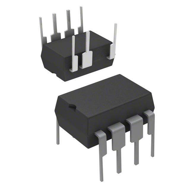
| 描述 | IC REG PWM CONV AC/DC TO-220F-6 |
| 产品分类 | |
| 品牌 | Sanken |
| 数据手册 | |
| 产品图片 |
|
| 产品型号 | STR-W6052S |
| rohs | 无铅 / 符合限制有害物质指令(RoHS)规范要求 |
| 产品系列 | - |
| 供应商器件封装 | TO-220-6L(成形) |
| 其它名称 | STR-W6052S DK |
| 功率(W) | 40W |
| 包装 | 管件 |
| 封装/外壳 | TO-220-7(成形引线),6 引线 |
| 工作温度 | -20°C ~ 115°C |
| 标准包装 | 50 |
| 电压-击穿 | 650V |
| 电压-输入 | 8.1 V ~ 32 V |
| 电压-输出 | - |
| 输出隔离 | 隔离 |
| 频率范围 | 60kHz ~ 74kHz |
.jpg)


- 商务部:美国ITC正式对集成电路等产品启动337调查
- 曝三星4nm工艺存在良率问题 高通将骁龙8 Gen1或转产台积电
- 太阳诱电将投资9.5亿元在常州建新厂生产MLCC 预计2023年完工
- 英特尔发布欧洲新工厂建设计划 深化IDM 2.0 战略
- 台积电先进制程称霸业界 有大客户加持明年业绩稳了
- 达到5530亿美元!SIA预计今年全球半导体销售额将创下新高
- 英特尔拟将自动驾驶子公司Mobileye上市 估值或超500亿美元
- 三星加码芯片和SET,合并消费电子和移动部门,撤换高东真等 CEO
- 三星电子宣布重大人事变动 还合并消费电子和移动部门
- 海关总署:前11个月进口集成电路产品价值2.52万亿元 增长14.8%


PDF Datasheet 数据手册内容提取
Off-Line PWM Controllers with Integrated Power MOSFET STR-W6000S Series General Descriptions Package The STR-W6000S series are power ICs for switching power supplies, incorporating a MOSFET and a current TO220F-6L mode PWM controller IC. The low standby power is accomplished by the automatic switching between the PWM operation in normal operation and the burst-oscillation under light load conditions. The product achieves high cost-performance power supply systems with few external components. Features Current Mode Type PWM Control Not to Scale Brown-In and Brown-Out function Auto Standby Function Lineup No Load Power Consumption < 30 mW Electrical Characteristics Operation Mode f = 67 kHz OSC(AVG) Normal Operation ----------------------------- PWM Mode Standby ---------------------------- Burst Oscillation Mode V R Products DSS DS(ON) Random Switching Function (min.) (max.) Slope Compensation Function STR-W6051S 3.95 Ω Leading Edge Blanking Function STR-W6052S 650 V 2.8 Ω Bias Assist Function STR-W6053S 1.9 Ω Audible Noise Suppression function during Standby STR-W6072S 800 V 3.6 Ω mode Protections Output Power, P * OUT ・Overcurrent Protection (OCP); Pulse-by-Pulse, P (Open frame) built-in compensation circuit to minimize OCP point Products OUT variation on AC input voltage AC230V AC85~265V ・Overload Protection (OLP); auto-restart STR-W6051S 45 W 30 W ・Overvoltage Protection (OVP); auto-restart STR-W6052S 60 W 40 W ・Thermal Shutdown Protection (TSD); auto-restart STR-W6053S 90 W 60 W STR-W6072S 50 W 32 W * The output power is actual continues power that is measured at 50 °C ambient. The peak output power can be 120 to 140 % of the Typical Application Circuit value stated here. Core size, ON Duty, and thermal design affect the output power. It may be less than the value stated here. VAC BR1 T1 D51 L51 VOUT(+) Applications C1 C6 R1 R54 PC1 R51 White goods P D1 S C51 R52 R55 C53 Office automation equipment U1 C52 R53 Industrial equipment D2 R2 U51 R56 STR-W6000S C2 D VOUT(-) D/ST2S/OCPVCCGNDFB/OLPBR RA 1 3 4567 RB C5 C3 C4 ROCP PC1 RC CY TC_STR-W6000S_1_R1 STR-W6000S - DS Rev.2.0 SANKEN ELECTRIC CO.,LTD. 1 Aug. 07, 2014 http://www.sanken-ele.co.jp/en/
STR-W6000S Series CONTENTS General Descriptions ----------------------------------------------------------------------- 1 1. Absolute Maximum Ratings --------------------------------------------------------- 3 2. Electrical Characteristics ------------------------------------------------------------ 4 3. Performance Curves ------------------------------------------------------------------ 5 3.1 Derating Curves --------------------------------------------------------------- 5 3.2 Ambient Temperature versus Power Dissipation Curves ------------ 6 3.3 MOSFET Safe Operating Area Curves ---------------------------------- 7 3.4 Transient Thermal Resistance Curves ----------------------------------- 8 4. Functional Block Diagram ----------------------------------------------------------- 9 5. Pin Configuration Definitions ------------------------------------------------------- 9 6. Typical Application Circuit -------------------------------------------------------- 10 7. Package Outline ----------------------------------------------------------------------- 11 8. Marking Diagram -------------------------------------------------------------------- 11 9. Operational Description ------------------------------------------------------------- 12 9.1 Startup Operation ----------------------------------------------------------- 12 9.2 Undervoltage Lockout (UVLO) ------------------------------------------- 13 9.3 Bias Assist Function --------------------------------------------------------- 13 9.4 Constant Output Voltage Control ---------------------------------------- 13 9.5 Leading Edge Blanking Function ---------------------------------------- 14 9.6 Random Switching Function ---------------------------------------------- 14 9.7 Automatic Standby Mode Function-------------------------------------- 14 9.8 Brown-In and Brown-Out Function ------------------------------------- 15 9.9 Overcurrent Protection Function (OCP) ------------------------------- 16 9.10 Overload Protection Function (OLP) ----------------------------------- 17 9.11 Overvoltage Protection (OVP) -------------------------------------------- 18 9.12 Thermal Shutdown Function (TSD) ------------------------------------- 18 10. Design Notes --------------------------------------------------------------------------- 18 10.1 External Components ------------------------------------------------------- 18 10.2 PCB Trace Layout and Component Placement ----------------------- 20 11. Pattern Layout Example ------------------------------------------------------------ 22 12. Reference Design of Power Supply ----------------------------------------------- 23 OPERATING PRECAUTIONS -------------------------------------------------------- 25 IMPORTANT NOTES ------------------------------------------------------------------- 26 STR-W6000S - DS Rev.2.0 SANKEN ELECTRIC CO.,LTD. 2 Aug. 07, 2014
STR-W6000S Series 1. Absolute Maximum Ratings The polarity value for current specifies a sink as "+," and a source as "−," referencing the IC. Unless otherwise specified T = 25 °C A Parameter Symbol Test Conditions Pins Rating Units Notes 5.0 STR-W6051S 7.0 STR-W6052S Drain Peak Current(1) I Single pulse 1 – 3 A DPEAK 7.5 STR-W6072S 9.5 STR-W6053S 5.0 STR-W6051S Maximum Switching Single pulse 7.0 STR-W6052S I 1 – 3 A Current(2) DMAX Ta= ‒20 to 125°C 7.5 STR-W6072S 9.5 STR-W6053S I =2.0A 47 STR-W6051S LPEAK I =2.3A 60 STR-W6072S Avalanche Energy(3)(4) E LPEAK 1 – 3 mJ AS I =2.3A 62 STR-W6052S LPEAK I =2.7A 86 STR-W6053S LPEAK S/OCP Pin Voltage V 3 – 5 − 2 to 6 V OCP VCC Pin Voltage V 4 – 5 32 V CC FB/OLP Pin Voltage V 6 – 5 − 0.3 to 14 V FB FB/OLP Pin Sink Current I 6 – 5 1.0 mA FB BR Pin Voltage V 7 – 5 − 0.3 to 7 V BR BR Pin Sink Current I 7 – 5 1.0 mA BR 22.3 STR-W6051S 23.6 STR-W6052S With infinite MOSFET Power heatsink 1 – 3 W P 25.8 STR-W6072S Dissipation(5) D1 26.5 STR-W6053S Without heatsink 1 – 3 1.3 W Control Part Power P V ×I 4 – 5 0.13 W Dissipation D2 CC CC Internal Frame Temperature T − − 20 to 115 °C in Operation F Operating Ambient T − − 20 to 115 °C Temperature OP Storage Temperature T − − 40 to 125 °C stg Junction Temperature T − 150 °C ch (1)Refer to 3.3 MOSFET Safe Operating Area Curves. (2) The maximum switching current is the drain current determined by the drive voltage of the IC and threshold voltage (V ) of the MOSFET. th (3) Refer to Figure 3-2 Avalanche Energy Derating Coefficient Curve. (4) Single pulse, V = 99 V, L = 20 mH DD (5) Refer to 3.2 Ta-P curves. D1 STR-W6000S - DS Rev.2.0 SANKEN ELECTRIC CO.,LTD. 3 Aug. 07, 2014
STR-W6000S Series 2. Electrical Characteristics The polarity value for current specifies a sink as "+," and a source as "−," referencing the IC. Unless otherwise specified, T = 25 °C, V = 18 V A CC Test Parameter Symbol Pins Min. Typ. Max. Units Notes Conditions Power Supply Startup Operation Operation Start Voltage V 4 – 5 13.8 15.3 16.8 V CC(ON) Operation Stop Voltage(1) V 4 – 5 7.3 8.1 8.9 V CC(OFF) Circuit Current in Operation I V = 12 V 4 – 5 − − 2.5 mA CC(ON) CC Startup Circuit Operation V 4 – 5 − 40 − V Voltage ST(ON) Startup Current I V = 13.5 V 4 – 5 − 3.9 − 2.5 − 1.1 mA STARTUP CC Startup Current Biasing I V CC 4 – 5 8.5 9.5 10.5 V Threshold Voltage CC(BIAS) = − 100 µA Normal Operation Average Switching f 1 – 5 60 67 74 kHz Frequency OSC(AVG) Switching Frequency Δf 1 – 5 − 5 − kHz Modulation Deviation Maximum ON Duty D 1 – 5 63 71 79 % MAX Protection Function Leading Edge Blanking Time t − − 390 − ns BW OCP Compensation DPC − − 18 − mV/μs Coefficient OCP Compensation ON Duty D − − 36 − % DPC OCP Threshold Voltage at V 3 – 5 0.70 0.78 0.86 V Zero ON Duty OCP(L) OCP Threshold Voltage at V V = 32 V 3 – 5 0.79 0.88 0.97 V 36% ON Duty OCP(H) CC Maximum Feedback Current I V = 12 V 6 – 5 − 340 − 230 − 150 µA FB(MAX) CC Minimum Feedback Current I 6 – 5 − 30 − 15 − 7 µA FB(MIN) FB/OLP pin Oscillation Stop V 6 – 5 0.85 0.95 1.05 V Threshold Voltage FB(STB) OLP Threshold Voltage V 6 – 5 7.3 8.1 8.9 V FB(OLP) OLP Operation Current I V = 12 V 4 – 5 − 300 − µA CC(OLP) CC OLP Delay Time t 6 – 5 54 68 82 ms OLP FB/OLP Pin Clamp Voltage V 6 – 5 11 12.8 14 V FB(CLAMP) Brown-In Threshold Voltage V V = 32 V 7 – 5 5.2 5.6 6 V BR(IN) CC Brown-Out Threshold V V = 32 V 7 – 5 4.45 4.8 5.15 V Voltage BR(OUT) CC BR Pin Clamp Voltage V V = 32 V 7 – 5 6 6.4 7 V BR(CLAMP) CC BR Function Disabling V V = 32 V 7 – 5 0.3 0.48 0.7 V Threshold BR(DIS) CC OVP Threshold Voltage V 4 – 5 26 29 32 V CC(OVP) Thermal Shutdown Operating T − 130 − − °C Temperature j(TSD) (1) V > V always. CC(BIAS) CC(OFF) STR-W6000S - DS Rev.2.0 SANKEN ELECTRIC CO.,LTD. 4 Aug. 07, 2014
STR-W6000S Series Test Parameter Symbol Pins Min. Typ. Max. Units Notes Conditions MOSFET Drain-to-Source Breakdown 650 − − STR-W605×S V 8 – 1 V Voltage DSS 800 − − STR-W6072S Drain Leakage Current I 8 – 1 − − 300 μA DSS − − 3.95 STR-W6051S − − 3.6 STR-W6072S On Resistance R 8 – 1 Ω DS(ON) − − 2.8 STR-W6052S − − 1.9 STR-W6053S Switching Time t 8 – 1 − − 250 ns f Thermal Resistance − − 2.63 STR-W6051S Channel to Frame Thermal − − 2.26 STR-W6052S θ − °C/W Resistance(2) ch-F − − 2.03 STR-W6072S − − 1.95 STR-W6053S (2) The thermal resistance between the channels of the MOSFET and the internal frame. 3. Performance Curves 3.1 Derating Curves 100 100 %) ( %) ent 80 ( 80 ci Areaefficient 60 ng Coeffi 60 g Co ati afe Operatinre Derating 40 perature Der 40 Seratu 20 Tem 20 mp AS e E T 0 0 25 50 75 100 125 150 0 25 50 75 100 125 Channel Temperature,Tch (°C) Channel Temperature,Tch (°C) Figure 3-1 SOA Temperature Derating Coefficient Curve Figure 3-2 Avalanche Energy Derating Coefficient Curve STR-W6000S - DS Rev.2.0 SANKEN ELECTRIC CO.,LTD. 5 Aug. 07, 2014
STR-W6000S Series 3.2 Ambient Temperature versus Power Dissipation Curves STR-W6051S STR-W6052S 30 30 R1 _ W) 25 P =22.3W W6051S_R1 ) 25 PD1=23.6W TR-W6052S on, P(D1 20 D1 With infinite heatsink PD1_STR- n, P(WD1 20 With infinite heatsink PD1_S pati 15 atio 15 ssi sip Di Dis er 10 r 10 w e w o P o P 5 Without heatsink 5 Without heatsink P =1.3W P =1.3W D1 D1 0 0 0 25 50 75 100 125 150 0 25 50 75 100 125 150 Ambient Temperature, T (°C ) Ambient Temperature, T (°C ) A A STR-W6053S STR-W6072S n, P(W)D1 223050 PD1=26.5W With infinite heatsink PD1_STR-W6053S_R1 P(W)D1 223050 PD1=25.8W With infinite heatsink PD1_STR-W6072S_R1 Dissipatio 15 ssipation, 15 er 10 Di 10 w r o we P 5 Without heatsink Po 5 Without heatsink P =1.3W P =1.3W D1 D1 0 0 0 25 50 75 100 125 150 0 25 50 75 100 125 150 Ambient Temperature, T (°C ) Ambient Temperature, T (°C ) A A STR-W6000S - DS Rev.2.0 SANKEN ELECTRIC CO.,LTD. 6 Aug. 07, 2014
STR-W6000S Series 3.3 MOSFET Safe Operating Area Curves When the IC is used, the safe operating area curve should be multiplied by the temperature derating coefficient derived from Figure 3-1. The broken line in the safe operating area curve is the drain current curve limited by on-resistance. Unless otherwise specified, T = 25 °C, Single pulse A STR-W6051S STR-W6052S 10 10 0.1ms R-W6051S_R1 0.1ms W6052S_R1 Drain Current, I(A)D 0.11 1ms SOA_ST Drain Current, I(A)D 0.11 1ms SOA_STR- 0.01 0.01 1 10 100 1000 1 10 100 1000 Drain-to-Source Voltage (V) Drain-to-Source Voltage (V) STR-W6053S STR-W6072S 100 R1 100 R1 _ _ S S (A)D 10 0.1ms A_STR-W6053 (A) 10 0.1ms A_STR-W6072 Current, I 1 1ms SO urrent, ID 1 1ms SO Drain 0.1 Drain C 0.1 0.01 0.01 1 10 100 1000 1 10 100 1000 Drain-to-Source Voltage (V) Drain-to-Source Voltage (V) STR-W6000S - DS Rev.2.0 SANKEN ELECTRIC CO.,LTD. 7 Aug. 07, 2014
STR-W6000S Series 3.4 Transient Thermal Resistance Curves STR-W6051S 10 R1 e _ stanc W6051S ResiW) 1 STR- mal °C/ TR_ ( her-c 0.1 Th nt θc e si n a Tr 0.01 1µ 10µ 100µ 1m 10m 100m Time (s) STR-W6052S 10 ResistanceW) 1 TR-W6052S_R1 al C/ R_S m° T ( erc Thh- 0.1 nt θc e si n a Tr 0.01 1µ 10µ 100µ 1m 10m 100m Time (s) STR-W6053S 10 ResistanceW) 1 TR-W6053S_R1 mal °C/ 0.1 TR_S ( erc h- Th nt θc 0.01 e si n a Tr 0.001 1µ 10µ 100µ 1m 10m 100m Time (s) STR-W6072S 10 nce S_R1 ResistaW) 1 R-W6072 mal (°C/ 0.1 TR_ST erc h- Th nt θc 0.01 e si n a Tr 0.001 1µ 10µ 100µ 1m 10m 100m Time (s) STR-W6000S - DS Rev.2.0 SANKEN ELECTRIC CO.,LTD. 8 Aug. 07, 2014
STR-W6000S Series 4. Functional Block Diagram VCC D/ST 4 Startup 1 UVLO REG VREG OVP TSD BR Brown-in 7 Brown-out 6.4V DRV PWM OSC S Q R OCP 7V VCC Drain peak current OLP compensation S/OCP FB/OLP Feedback LEB 3 6 control 12.8V Slope GND compensation 5 BD_STR-W6000S_R1 5. Pin Configuration Definitions Pin Name Descriptions 1 D/ST 1 D/ST MOSFET drain and startup current input 2 − (Pin removed) 3 S/OCP MOSFET source and overcurrent protection 4 VCC 3 S/OCP (OCP) signal input 5 GND Power supply voltage input for control part and 6 FB/OLP 4 VCC overvoltage protection (OVP) signal input 7 BR 5 GND Ground Constant voltage control signal input and over (LF2003) 6 FB /OLP load protection (OLP) signal input 7 BR Brown-In and Brown-Out detection voltage input STR-W6000S - DS Rev.2.0 SANKEN ELECTRIC CO.,LTD. 9 Aug. 07, 2014
STR-W6000S Series 6. Typical Application Circuit The following drawings show circuits enabled and disabled the Brown-In/Brown-Out function. The PCB traces D/ST pins should be as wide as possible, in order to enhance thermal dissipation. In applications having a power supply specified such that D/ST pin has large transient surge voltages, a clamp snubber circuit of a capacitor-resistor-diode (CRD) combination should be added on the primary winding P, or a damper snubber circuit of a capacitor (C) or a resistor-capacitor (RC) combination should be added between the D/ST pin and the S/OCP pin. L51 BR1 CRD clamp snubber T1 D51 VOUT VAC (+) C6 R1 R54 PC1 R51 C1 P R55 C51 D1 S R52 C53 C52 R53 U51 R56 STR-W6000S RA (-) P P L D/ST2S/OCVCCGNDFB/OBR RB 1 3 4 5 6 7 D2 R2 C5 C2 D PC1 ROCP C3 RC C4 C(CR) CY damper snubber TC_STR-W6000S_2_R1 Figure 6-1 Typical application circuit (enabled Brown-In/Brown-Out function, DC line detection) L51 BR1 CRD clamp snubber T1 D51 VOUT VAC (+) C6 R1 R54 PC1 R51 C1 P R55 C51 D1 S R52 C53 C52 R53 U51 R56 STR-W6000S (-) P P L T CCDO D/S2S/OVCGNFB/BR 1 3 4 5 6 7 D2 R2 C5 C2 D PC1 ROCP C3 C(RC) damper snubber CY TC_STR-W6000S_3_R1 Figure 6-2 Typical application circuit (disabled Brown-In/Brown-Out function) STR-W6000S - DS Rev.2.0 SANKEN ELECTRIC CO.,LTD. 10 Aug. 07, 2014
STR-W6000S Series 7. Package Outline TO220F-6L The pin 2 is removed to provide greater creepage and clearance isolation between the high voltage pin (pin 1: D/ST) and the low voltage pin (pin 3: S/OCP). 10.0±0.2 4.2±0.2 Gate burr 2.8±0.2 0.5 2 0. ± 4 0.2 ± .9 7 2 6.9±0.3 3.2±0.φ 1 2.6±0.1 (Dimensionsfromroot) 5 2.8 6-0.74±0.15 ±0. .0 5 5 6-0.65+-00..21 R-en5.4)d (2-R1) 10.4±0. ( 0.45+0.2 6×P1.27±0.15=7.62±0.15 -0.1 (Dimensionsfromroot) 5.08±0.6 (Dimensionsbetweentips) 0.5 0.5 0.5 0.5 Front view Side view 1 2 3 4 5 6 7 NOTE S: 1) Di mension is in millimeters 2) Le adform: LF No.2003 3) Ga te burr indicates protrusion of 0.3 mm (max). 4) Pb-free. Device composition compliant with the RoHS directive 8. Marking Diagram STR W 6 0 × × S Part Number Y M D D X Lot Number 2 1 3 7 Y is the last digit of the year (0 to 9) M is the month (1 to 9, O, N or D) DD is a day (01 to 31) X is the Sanken Control Symbol STR-W6000S - DS Rev.2.0 SANKEN ELECTRIC CO.,LTD. 11 Aug. 07, 2014
STR-W6000S Series 9. Operational Description With Brown-In / Brown-Out function When BR pin voltage is more than V = 0.48 V BR(DIS) All of the parameter values used in these descriptions and less than V = 5.6 V, the Bias Assist Function BR(IN) are typical values, unless they are specified as (refer to Section 9.3) is disabled. Thus, VCC pin minimum or maximum. voltage repeats increasing to V and decreasing to CC(ON) With regard to current direction, "+" indicates sink V (shown in Figure 9-3). When BR pin voltage CC(OFF) current (toward the IC) and "–" indicates source becomes V or more, the IC starts switching BR(IN) current (from the IC). operation. 9.1 Startup Operation BR1 T1 VAC Figure 9-1 shows the circuit around IC. Figure 9-2 C1 P shows the start up operation. The IC incorporates the startup circuit. The circuit is 1 connected to D/ST pin. When D/ST pin voltage reaches to Startup Circuit Operation Voltage V = 40 V, the D/ST D2 R2 ST(ON) U1 4 startup circuit starts operation. VCC During the startup process, the constant current, C2 V D I = − 2.5 mA, charges C2 at VCC pin. When D STARTUP 5 VCC pin voltage increases to VCC(ON) = 15.3 V, the BR GND control circuit starts operation. 7 During the IC operation, the voltage rectified the auxiliary winding voltage, V , of Figure 9-1 becomes a D power source to the VCC pin. After switching operation Figure 9-1 VCC pin peripheral circuit begins, the startup circuit turns off automatically so that (Without Brown-In / Brown-Out) its current consumption becomes zero. The approximate value of auxiliary winding voltage is about 15 V to 20 V, taking account of the winding turns VCC pin of D winding so that VCC pin voltage becomes voltage Equation (1) within the specification of input and output V CC(ON) voltage variation of power supply. V (max.)V V (min.) CC(BIAS) CC CC(OVP) t START Drain current, I ⇒10.5 (V) VCC 26 (V) (1) D The oscillation start timing of IC depends on Brown-In / Brown-Out function (refer to Section 9.8). Figure 9-2 Startup operation (Without Brown-In / Brown-Out) Without Brown-In / Brown-Out function (BR pin voltage is V = 0.48 V or less) BR(DIS) When VCC pin voltage increases to V , the IC VCC pin CC(ON) starts switching operation, As shown in Figure 9-2. voltage t START V CC(ON) The startup time of IC is determined by C2 capacitor V CC(OFF) value. The approximate startup time t (shown in START Figure 9-2) is calculated as follows: BR pin V -V t C2× CC(ON) CC(INT) (2) voltage VBR(IN) START I STRATUP where, Drain current, tSTART : Startup time of IC (s) ID V : Initial voltage on VCC pin (V) CC(INT) Figure 9-3 Startup operation (With Brown-In / Brown-Out) STR-W6000S - DS Rev.2.0 SANKEN ELECTRIC CO.,LTD. 12 Aug. 07, 2014
STR-W6000S Series 9.2 Undervoltage Lockout (UVLO) biasing voltage, V = 9.5 V. While the Bias Assist CC(BIAS) function is activated, any decrease of the VCC pin Figure 9-4 shows the relationship of VCC pin voltage voltage is counteracted by providing the startup current, and circuit current I . When VCC pin voltage decreases CC I , from the startup circuit. Thus, the VCC pin STARTUP to V = 8.1 V, the control circuit stops operation by CC(OFF) voltage is kept almost constant. UVLO (Undervoltage Lockout) circuit, and reverts to By the Bias Assist function, the value of C2 is the state before startup. allowed to be small and the startup time becomes shorter. Also, because the increase of VCC pin voltage becomes Circuit current, I faster when the output runs with excess voltage, the CC response time of the OVP function becomes shorter. I CC(ON) It is necessary to check and adjust the startup process based on actual operation in the application, so that poor starting conditions may be avoided. Stop Start 9.4 Constant Output Voltage Control The IC achieves the constant voltage control of the VCC pin power supply output by using the current-mode control V V CC(OFF) CC(ON) voltage method, which enhances the response speed and provides the stable operation. Figure 9-4 Relationship between The FB/OLP pin voltage is internally added the slope VCC pin voltage and I compensation at the feedback control (refer to Section 4 CC Functional Block Diagram), and the target voltage, V , SC is generated. The IC compares the voltage, V , of a ROCP 9.3 Bias Assist Function current detection resistor with the target voltage, VSC, by the internal FB comparator, and controls the peak value Figure 9-5 shows VCC pin voltage behavior during of V so that it gets close to V , as shown in Figure ROCP SC the startup period. 9-6 and Figure 9-7. After VCC pin voltage increases to V = 15.3 V CC(ON) at startup, the IC starts the operation. Then circuit current increases and VCC pin voltage decreases. At the U1 same time, the auxiliary winding voltage V increases in D proportion to output voltage. These are all balanced to S/OCP GND FB/OLP produce VCC pin voltage. 3 5 6 VCC pin Startup success PC1 voltage IC starts operation Target operating VROCP ROCP C3 IFB V voltage CC(ON) V Increase with rising of CC(BIAS) output voltage Figure 9-6 FB/OLP pin peripheral circuit Bias assist period V CC(OFF) Target voltage including Startup failure Slope Compensation Time - VSC Figure 9-5 VCC pin voltage during startup period + V ROCP The surge voltage is induced at output winding at Voltage on both FB Comparator turning off a power MOSFET. When the output load is sides of ROCP light at startup, the surge voltage causes the unexpected feedback control. This results the lowering of the output Drain current, power and VCC pin voltage. When the VCC pin voltage I decreases to V = 8.1 V, the IC stops switching D CC(OFF) operation and a startup failure occurs. In order to prevent this, the Bias Assist function is activated when the VCC Figure 9-7 Drain current, I , and FB comparator D pin voltage decreases to the startup current threshold operation in steady operation STR-W6000S - DS Rev.2.0 SANKEN ELECTRIC CO.,LTD. 13 Aug. 07, 2014
STR-W6000S Series Light load conditions In peak-current-mode control method, there is a case When load conditions become lighter, the output that the power MOSFET turns off due to unexpected voltage, V , increases. Thus, the feedback current response of FB comparator or overcurrent protection OUT from the error amplifier on the secondary-side also circuit (OCP) to the steep surge current in turning on a increases. The feedback current is sunk at the FB/OLP power MOSFET. pin, transferred through a photo-coupler, PC1, and the In order to prevent this response to the surge voltage FB/OLP pin voltage decreases. Thus, V decreases, in turning-on the power MOSFET, the Leading Edge SC and the peak value of V is controlled to be low, Blanking, t = 390 ns is built-in. During t , the OCP ROCP BW BW and the peak drain current of I decreases. threshold voltage becomes about 1.7 V which is higher D This control prevents the output voltage from than the normal OCP threshold voltage (refer to Section increasing. 9.9). Heavy load conditions When load conditions become greater, the IC 9.6 Random Switching Function performs the inverse operation to that described above. The IC modulates its switching frequency randomly Thus, V increases and the peak drain current of I SC D by superposing the modulating frequency on f in increases. OSC(AVG) normal operation. This function reduces the conduction This control prevents the output voltage from noise compared to others without this function, and decreasing. simplifies noise filtering of the input lines of power supply. In the current mode control method, when the drain current waveform becomes trapezoidal in continuous operating mode, even if the peak current level set by the 9.7 Automatic Standby Mode Function target voltage is constant, the on-time fluctuates based on the initial value of the drain current. Automatic standby mode is activated automatically This results in the on-time fluctuating in multiples of when the drain current, I , reduces under light load the fundamental operating frequency as shown in Figure D conditions, at which I is less than 15 % to 20 % of the 9-8. This is called the subharmonics phenomenon. D maximum drain current (it is in the OCP state). The In order to avoid this, the IC incorporates the Slope operation mode becomes burst oscillation, as shown in Compensation function. Because the target voltage is Figure 9-9. Burst oscillation mode reduces switching added a down-slope compensation signal, which reduces losses and improves power supply efficiency because of the peak drain current as the on-duty gets wider relative periodic non-switching intervals. to the FB/OLP pin signal to compensate V , the SC subharmonics phenomenon is suppressed. Even if subharmonic oscillations occur when the IC Output current, Burst oscillation I has some excess supply being out of feedback control, OUT such as during startup and load shorted, this does not affect performance of normal operation. Below several kHz Target voltage Drain current, without Slope Compensation I D Normal Standby Normal operation operation operation Figure 9-9 Auto Standby mode timing t t ON1 ON2 Generally, to improve efficiency under light load conditions, the frequency of the burst oscillation mode T T T becomes just a few kilohertz. Because the IC suppresses the peak drain current well during burst oscillation mode, Figure 9-8 Drain current, I , waveform D audible noises can be reduced. in subharmonic oscillation If the VCC pin voltage decreases to V = 9.5 V CC(BIAS) during the transition to the burst oscillation mode, the Bias Assist function is activated and stabilizes the 9.5 Leading Edge Blanking Function Standby mode operation, because I is provided to STARTUP the VCC pin so that the VCC pin voltage does not The IC uses the peak-current-mode control method decrease to V . for the constant voltage control of output. CC(OFF) STR-W6000S - DS Rev.2.0 SANKEN ELECTRIC CO.,LTD. 14 Aug. 07, 2014
STR-W6000S Series However, if the Bias Assist function is always There are two types of detection method as follows: activated during steady-state operation including standby mode, the power loss increases. Therefore, the VCC pin voltage should be more than VCC(BIAS), for 9.8.1 DC Line Detection example, by adjusting the turns ratio of the auxiliary winding and secondary winding and/or reducing the Figure 9-11 shows BR pin peripheral circuit of DC value of R2 in Figure 10-2 (refer to Section 10.1 line detection. There is a ripple voltage on C1 Peripheral Components for a detail of R2). occurring at a half period of AC cycle. In order to detect each peak of the ripple voltage, the time constant of R and C4 should be shorter than a half C period of AC cycle. 9.8 Brown-In and Brown-Out Function Since the cycle of the ripple voltage is shorter than This function stops switching operation when it t , the switching operation does not stop when only OLP detects low input line voltage, and thus prevents the bottom part of the ripple voltage becomes lower excessive input current and overheating. than V . BR(OUT) This function turns on and off switching operation Thus it minimizes the influence of load conditions according to the BR pin voltage detecting the AC input on the voltage detection. voltage. When BR pin voltage becomes more than V = 0.48 V, this function is activated. BR(DIS) BR1 V Figure 9-10 shows waveforms of the BR pin voltage AC and the drain currnet. R A Even if the IC is in the operating state that the VCC C1 U1 pin voltage is VCC(OFF) or more, when the AC input VDC RB 7 voltage decreases from steady-state and the BR pin BR GND voltage falls to V = 4.8 V or less for the OLP BR(OUT) R C4 5 Delay Time, t = 68 ms, the IC stops switching C OLP operation. When the AC input voltage increases and the BR pin voltage reaches VBR(IN) = 5.6 V or more in the operating Figure 9-11 DC line detection state that the VCC pin voltage is V or more, the IC CC(OFF) starts switching operation. The components around BR pin: In case the Brown-In and Brown-Out function is ・ R and R are a few megohms. Because of high A B unnecessary, connect the BR pin trace to the GND pin voltage applied and high resistance, it is trace so that the BR pin voltage is V or less. BR(DIS) recommended to select a resistor designed against This function is disabled during switching operation electromigration or use a combination of resistors stop period in burst oscillation mode. When the BR pin in series for that to reduce each applied voltage, voltage falls to V or less in burst oscillation mode BR(OUT) according to the requirement of the application. and the sum of switching operation period becomes tOLP = 68 ms or more, the IC stops switching operation. ・ RC is a few hundred kilohms ・ C4 is 470 pF to 2200 pF for high frequency noise BR pin voltage reduction V BR(IN) Neglecting the effect of both input resistance and V BR(OUT) forward voltage of rectifier diode, the reference value of C1 voltage when Brown-In and Brown-Out Drain current, tOLP I function is activated is calculated as follows: D R R V V 1 A B Figure 9-10 BR pin voltage and drain current waveforms DC(OP) BR(TH) RC (3) where, V : C1 voltage when Brown-In and DC(OP) Brown-Out function is activated V : Any one of threshold voltage of BR pin BR(TH) (see Table 9-1) STR-W6000S - DS Rev.2.0 SANKEN ELECTRIC CO.,LTD. 15 Aug. 07, 2014
STR-W6000S Series Table 9-1 BR pin threshold voltage Neglecting the effect of input resistance is zero, the reference effective value of AC input voltage when Value Parameter Symbol Brown-In and Brown-Out function is activated is (Typ.) calculated as follows: Brown-In Threshold Voltage V 5.6 V BR(IN) Brown-Out Threshold Voltage V 4.8 V R R BR(OUT) V V 1 A B (5) AC(OP)RMS 2 BR(TH) RC V can be expressed as the effective value of AC DC(OP) input voltage using Equation (4). where, V :The effective value of AC input voltage AC(OP)RMS 1 when Brown-In and Brown-Out function V V (4) AC(OP)RMS 2 DC(OP) is activated V :Any one of threshold voltage of BR pin BR(TH) (see Table 9-1) R , R , R and C4 should be selected based on actual A B C operation in the application. R , R , R and C4 should be selected based on A B C actual operation in the application. 9.8.2 AC Line Detection Figure 9-12 shows BR pin peripheral circuit of AC 9.9 Overcurrent Protection Function line detection. (OCP) In order to detect the AC input voltage, the time constant of R and C4 should be longer than the Overcurrent Protection Function (OCP) detects each C period of AC cycle. Thus the response of BR pin drain peak current level of a power MOSFET on detection becomes slow compared with the DC line pulse-by-pulse basis, and limits the output power when detection. the current level reaches to OCP threshold voltage. This method detects the AC input voltage, and thus During Leading Edge Blanking Time (tBW), OCP is it minimizes the influence from load conditions. disabled. When power MOSFET turns on, the surge voltage width of S/OCP pin should be less than t , as BW shown in Figure 9-13. In order to prevent surge voltage, V BR1 pay extra attention to ROCP trace layout (refer to Section AC ). In addition, if a C (RC) damper snubber of Figure RA 4 9-14 is used, reduce the capacitor value of damper RS VCC U1 snubber. VDC RB C1 7 BR GND tBW R C4 5 C V ’ OCP Figure 9-12 AC line detection The components around BR pin: Surge pulse voltage width at turning on ・ R and R are a few megohms. Because of high A B voltage applied and high resistance, it is Figure 9-13 S/OCP pin voltage recommended to select a resistor designed against electromigration or use a combination of resistors in series for that to reduce each applied voltage, according to the requirement of the application. ・ R is a few hundred kilohms C ・ R must be adjusted so that the BR pin voltage is S more than V = 0.48 V when the VCC pin BR(DIS) voltage is V = 8.1 V CC(OFF) ・ C4 is 0.22 μF to 1 μF for averaging AC input voltage and high frequency noise reduction. STR-W6000S - DS Rev.2.0 SANKEN ELECTRIC CO.,LTD. 16 Aug. 07, 2014
STR-W6000S Series C(RC) V 'V DPCONTime OCP OCP(L) Damper snubber T1 ONDuty D51 V DPC C1 C51 OCP(L) f (6) OSC(AVG) 1 where, D/ST V : OCP Threshold Voltage at Zero ON Duty OCP(L) U1 C(RC) DPC: OCP Compensation Coefficient S/OCP Damper snubber ONTime: On-time of power MOSFET 3 ONDuty: On duty of power MOSFET R OCP f : Average PWM Switching Frequency OSC(AVG) Figure 9-14 Damper snubber 9.10 Overload Protection Function (OLP) Figure 9-16 shows the FB/OLP pin peripheral circuit, < Input Compensation Function > and Figure 9-17 shows each waveform for OLP ICs with PWM control usually have some propagation operation. delay time. The steeper the slope of the actual drain current at a high AC input voltage is, the larger the detection voltage of actual drain peak current is, U1 compared to V . Thus, the peak current has some OCP variation depending on the AC input voltage in OCP GND FB/OLP VCC state. 3 6 4 In order to reduce the variation of peak current in D2 R2 OCP state, the IC incorporates a built-in Input PC1 Compensation function. The Input Compensation Function is the function of C3 C2 correction of OCP threshold voltage depending with AC D input voltage, as shown in Figure 9-15. When AC input voltage is low (ON Duty is broad), the OCP threshold voltage is controlled to become high. Figure 9-16 FB/OLP pin peripheral circuit The difference of peak drain current become small compared with the case where the AC input voltage is high (ON Duty is narrow). Non-switching interval The compensation signal depends on ON Duty. The VCC pin voltage relation between the ON Duty and the OCP threshold V CC(ON) voltage after compensation V ' is expressed as OCP V Equation (6). When ON Duty is broader than 36 %, the CC(OFF) V ' becomes a constant value V = 0.88 V OCP OCP(H) FB/OLP pin voltage 1.0 V tOLP tOLP FB(OLP) r e aft V Voltage n, V'OCP VOOCCPP((HL)) Drain currenItD, old satio hn se hremp Figure 9-17 OLP operational waveforms To CP c DDPC DMAX O When the peak drain current of I is limited by OCP D 0.5 operation, the output voltage, V , decreases and the 0 50 100 OUT ON Duty (%) feedback current from the secondary photo-coupler becomes zero. Thus, the feedback current, I , charges FB C3 connected to the FB/OLP pin and the FB/OLP pin Figure 9-15 Relationship between ON Duty and Drain voltage increases. When the FB/OLP pin voltage Current Limit after compensation STR-W6000S - DS Rev.2.0 SANKEN ELECTRIC CO.,LTD. 17 Aug. 07, 2014
STR-W6000S Series increases to V = 8.1 V or more for the OLP delay 9.12 Thermal Shutdown Function (TSD) FB(OLP) time, t = 68 ms or more, the OLP function is OLP When the temperature of control circuit increases to activated, the IC stops switching operation. T = 130 °C or more, Thermal Shutdown function During OLP operation, Bias Assist Function is j(TSD) (TSD) is activated, the IC stops switching operation. disabled. Thus, VCC pin voltage decreases to V , CC(OFF) During TSD operation, the Bias Assist function is the control circuit stops operation. After that, the IC disabled, the intermittent operation by UVLO is repeated reverts to the initial state by UVLO circuit, and the IC (refer to Section 9.10). When the fault condition is starts operation when VCC pin voltage increases to removed and the temperature decreases to less than V by startup current. Thus the intermittent CC(ON) T , the IC returns to normal operation automatically. operation by UVLO is repeated in OLP state. j(TSD) This intermittent operation reduces the stress of parts such as power MOSFET and secondary side rectifier diode. In addition, this operation reduces power consumption because the switching period in this 10. Design Notes intermittent operation is short compared with oscillation stop period. When the abnormal condition is removed, the IC returns to normal operation automatically. 10.1 External Components Take care to use properly rated, including derating as necessary and proper type of components. 9.11 Overvoltage Protection (OVP) When a voltage between VCC pin and GND pin CRD clamp snubber increases to V = 29 V or more, OVP function is BR1 T1 CC(OVP) VAC activated, the IC stops switching operation. During OVP C6 R1 C1 operation, the Bias Assist function is disabled, the P intermittent operation by UVLO is repeated (refer to D1 Section 9.10). When the fault condition is removed, the U1 IC returns to normal operation automatically (refer to FigIunr ec a9s-e1 8t)h. e VCC pin voltage is provided by using D/ST1 2S/OCP3VCC4GND5FB/OLP6BR7 RRAB D2 R2 auxiliary winding of transformer, the overvoltage conditions such as output voltage detection circuit open C5 D C2 can be detected because the VCC pin voltage is C(RC) ROCP C3 C4 RC proportional to output voltage. The approximate value of sdnaumbpbeerr PC1 output voltage V in OVP condition is calculated OUT(OVP) by using Equation (7). Figure 10-1 The IC peripheral circuit V V OUT(NORMAL) 29 (V) (7) Input and Output Electrolytic Capacitor OUT(OVP) V Apply proper derating to ripple current, voltage, and CC(NORMAL) temperature rise. Use of high ripple current and low impedance types, designed for switch mode power where, supplies, is recommended. V : Output voltage in normal operation OUT(NORMAL) V : VCC pin voltage in normal operation CC(NORMAL) S/OCP Pin Peripheral Circuit In Figure 10-1, R is the resistor for the current VCC pin voltage OCP detection. A high frequency switching current flows V CC(OVP) to R , and may cause poor operation if a high OCP inductance resistor is used. Choose a low inductance VCC(ON) and high surge-tolerant type. V CC(OFF) VCC Pin Peripheral Circuit The value of C2 in Figure 10-1 is generally Drain current, recommended to be 10µ to 47μF (refer to Section 9.1 I Startup Operation, because the startup time is D determined by the value of C2). In actual power supply circuits, there are cases in which the VCC pin voltage fluctuates in proportion to Figure 9-18 OVP operational waveforms the output current, I (see Figure 10-2), and the OUT Overvoltage Protection function (OVP) on the VCC STR-W6000S - DS Rev.2.0 SANKEN ELECTRIC CO.,LTD. 18 Aug. 07, 2014
STR-W6000S Series pin may be activated. This happens because C2 is ・ A damper snubber circuit of a capacitor (C) or a charged to a peak voltage on the auxiliary winding D, resistor-capacitor (RC) combination should be which is caused by the transient surge voltage coupled added between the D/ST pin and the S/OCP pin. from the primary winding when the power MOSFET In case the damper snubber circuit is added, this turns off. components should be connected near D/ST pin For alleviating C2 peak charging, it is effective to add and S/OCP pin. some value R2, of several tenths of ohms to several ohms, in series with D2 (see Figure 10-1). The Peripheral circuit of secondary side shunt regulator optimal value of R2 should be determined using a Figure 10-3 shows the secondary side detection circuit transformer matching what will be used in the actual with the standard shunt regulator IC (U51). application, because the variation of the auxiliary C52 and R53 are for phase compensation. The value winding voltage is affected by the transformer of C52 and R53 are recommended to be around structural design. 0.047μF to 0.47μF and 4.7 kΩ to 470 kΩ, respectively. They should be selected based on actual operation in the application. VCC pin voltage Without R2 L51 T1 D51 VOUT (+) With R2 R54 PC1 R51 Output current, I OUT R55 C51 R52 Figure 10-2 Variation of VCC pin voltage and power S C53 C52 R53 FB/OLP Pin Peripheral Circuit C3 is for high frequency noise reduction and phase U51 compensation, and should be connected close to these R56 pins. The value of C3 is recommended to be about (-) 2200 pF to 0.01µF, and should be selected based on actual operation in the application. Figure 10-3 Peripheral circuit of secondary side shunt BR pin peripheral circuit regulator (U51) Because R and R (see Figure 10-1) are applied high A B voltage and are high resistance, the following should be Transformer considered according to the requirement of the Apply proper design margin to core temperature rise application: by core loss and copper loss. ▫ Select a resistor designed against electromigration, Because the switching currents contain high or frequency currents, the skin effect may become a ▫ Use a combination of resistors in series for that to consideration. reduce each applied voltage Choose a suitable wire gauge in consideration of the RMS current and a current density of 4 to 6 A/mm2. See the section 9.8 about the AC input voltage If measures to further reduce temperature are still detection function and the components around BR pin. necessary, the following should be considered to When the detection resistor (R , R , R ) value is A B C increase the total surface area of the wiring: decreased and the C4 value is increased to prevent ▫ Increase the number of wires in parallel. unstable operation resulting from noise at the BR pin, ▫ Use litz wires. pay attention to the low efficiency and the slow ▫ Thicken the wire gauge. response of BR pin. In the following cases, the surge of VCC pin Snubber Circuit voltage becomes high. In case the surge voltage of V is large, the circuit DS ▫ The surge voltage of primary main winding, P, is should be added as follows (see Figure 10-1); high (low output voltage and high output current ・ A clamp snubber circuit of a capacitor-resistor- power supply designs) diode (CRD) combination should be added on the ▫ The winding structure of auxiliary winding, D, is primary winding P. susceptible to the noise of winding P. STR-W6000S - DS Rev.2.0 SANKEN ELECTRIC CO.,LTD. 19 Aug. 07, 2014
STR-W6000S Series 10.2 PCB Trace Layout and Component When the surge voltage of winding D is high, the Placement VCC pin voltage increases and the Overvoltage Protection function (OVP) may be activated. In Since the PCB circuit trace design and the component transformer design, the following should be layout significantly affects operation, EMI noise, and considered; power dissipation, the high frequency PCB trace should ▫ The coupling of the winding P and the secondary be low impedance with small loop and wide trace. output winding S should be maximized to reduce the In addition, the ground traces affect radiated EMI noise, leakage inductance. and wide, short traces should be taken into account. ▫ The coupling of the winding D and the winding S Figure 10-5 shows the circuit design example. should be maximized. ▫ The coupling of the winding D and the winding P (1) Main Circuit Trace Layout should be minimized. This is the main trace containing switching currents, and thus it should be as wide trace and small loop as In the case of multi-output power supply, the possible. coupling of the secondary-side stabilized output If C1 and the IC are distant from each other, placing winding, S1, and the others (S2, S3…) should be a capacitor such as film capacitor (about 0.1 μF and maximized to improve the line-regulation of those with proper voltage rating) close to the transformer outputs. or the IC is recommended to reduce impedance of the high frequency current loop. Figure 10-4 shows the winding structural examples of two outputs. (2) Control Ground Trace Layout Winding structural example (a): Since the operation of IC may be affected from the S1 is sandwiched between P1 and P2 to large current of the main trace that flows in control maximize the coupling of them for surge ground trace, the control ground trace should be reduction of P1 and P2. separated from main trace and connected at a single D is placed far from P1 and P2 to minimize the point grounding of point A in Figure 10-5 as close to coupling to the primary for the surge reduction of the ROCP pin as possible. D. (3) VCC Trace Layout Winding structural example (b) This is the trace for supplying power to the IC, and P1 and P2 are placed close to S1 to maximize the thus it should be as small loop as possible. If C2 and coupling of S1 for surge reduction of P1 and P2. the IC are distant from each other, placing a D and S2 are sandwiched by S1 to maximize the capacitor such as film capacitor C (about 0.1 μF to f coupling of D and S1, and that of S1 and S2. 1.0 μF) close to the VCC pin and the GND pin is This structure reduces the surge of D, and recommended. improves the line-regulation of outputs. (4) R Trace Layout OCP R should be placed as close as possible to the OCP S/OCP pin. The connection between the power Margin tape ground of the main trace and the IC ground should be at a single point ground (point A in Figure 10-5) n obbi P1 S1 P2 S2 D which is close to the base of ROCP. B Margin tape (5) Peripheral components of the IC The components for control connected to the IC Winding structural example (a) should be placed as close as possible to the IC, and should be connected as short as possible to the each Margin tape pin. bin P1 S1 D S2 S1 P2 (6) Secondary Rectifier Smoothing Circuit Trace b Bo Layout: This is the trace of the rectifier smoothing loop, Margin tape carrying the switching current, and thus it should be Winding structural example (b) as wide trace and small loop as possible. If this trace is thin and long, inductance resulting from the loop Figure 10-4 Winding structural examples may increase surge voltage at turning off the power MOSFET. Proper rectifier smoothing trace layout helps to increase margin against the power MOSFET STR-W6000S - DS Rev.2.0 SANKEN ELECTRIC CO.,LTD. 20 Aug. 07, 2014
STR-W6000S Series breakdown voltage, and reduces stress on the clamp snubber circuit and losses in it. (7) Thermal Considerations Because the power MOSFET has a positive thermal coefficient of R , consider it in thermal design. DS(ON) Since the copper area under the IC and the D/ST pin trace act as a heatsink, its traces should be as wide as possible. (1)Main trace should be wide (6)Main trace of secondary side should trace and small loop be wide trace and small loop T1 C6 R1 D51 C1 P C51 D1 S U1 RA P P L T CCDO (3) Loop of the power D/S2S/OVCGNFB/BR RB supply should be small 1 3 4 5 6 7 D2 R2 C5 PC1 C2 D (7)Twriadcee foofr Dhe/SatT r epliena ssheould be ROCP C3 C4 RC A CY (4)ROCP should be as (2) Control GND trace should be (5)The components connected to the IC should close to S/OCP pin connected at a single point as be as close to the IC as possible, and should as possible. close to the ROCP as possible be connected as short as possible Figure 10-5 Peripheral circuit example around the IC STR-W6000S - DS Rev.2.0 SANKEN ELECTRIC CO.,LTD. 21 Aug. 07, 2014
STR-W6000S Series 11. Pattern Layout Example The following show the PCB pattern layout example and the schematic of the four outputs circuit using STR-W6000S series without Brown-In and Brown-Out function. The above circuit symbols correspond to these of Figure 11-1. Only the parts in the schematic are used. Other parts in PCB are leaved open. C11 and D4 are shorted. Figure 11-1 PCB circuit trace layout example T1 D56 CN51 3 OUT4(+) S4 C64 C65 R66 4 OUT4(-) CN1 1 F1 L1 JW1 D54 JW54 Z54 L53 JW51 Z53 5 OUT3(+) C2 R63 C1 C4 D1 TH1 JW3 S3 C60C61 C62 JW56 D55 R64 C63 R65 C3 6 OUT3(-) 3 C5 C6 R1 D52JW55 JW52 Z52 L52 8 OUT2(+) TK1 P1 D53 R60 S2 C56 JW61 R62 D2 C57 C58 R61 C59 7 OUT2(-) JW53 R59 R58 Z1 D4 D51 JJWW5578 L51 R57 STR-W6000S D3 R2 2 OUT1(+) P LP C8 C7 D C51 R51 JW59 D/ST2S/OCVCCGNDFB/OBR PC1 R54 1 3 4 5 6 7 R52 R55 S1 C52 C53 C55 C54 R53 C13 Z51 PC1 R56 R5 C11 C10 1 OUT1(-) C12 TK2 Figure 11-2 Circuit schematic for PCB circuit trace layout STR-W6000S - DS Rev.2.0 SANKEN ELECTRIC CO.,LTD. 22 Aug. 07, 2014
STR-W6000S Series 12. Reference Design of Power Supply As an example, the following show the power supply specification, the circuit schematic, the bill of materials, and the transformer specification. Power supply specification IC STR-W6053S Input voltage AC85 V to AC265 V Maximum output power 56 W (70.4 W ) PEAK Output 1 8 V / 2.5 A Output 2 12 V / 3 A (4.2 A ) PEAK Circuit schematic VAC F1 L1 C1 C2 BR1 VDC T1 D52 OUT1(+) 12V/4.2A C3 C4 R1 P1 S1 C55 TH1 C56 C57 R57 P2 D1 S2 OUT1(-) L51 D51 OUT2(+) R4 8V/2.5A U1 R54 C51 PC1 R51 P R5 P L T CCDO R55 D/S2S/OVCGNFB/BR R6 S3 C52 R52 C54 1 3 4 5 6 7 D2 R3 C53 R53 C5 C6 D U51 R56 PC1 R2 C7 R7 OUT2(-) C8 C9 TC_STR-W6000S_4_R1 Bill of materials Recommended Recommended Symbol Part type Ratings(1) Symbol Part type Ratings(1) Sanken Parts Sanken Parts F1 Fuse AC 250 V, 6 A PC1 Photo-coupler PC123 or equiv L1 (2) CM inductor 2.2 mH U1 IC - STR-W6053S See TH1 (2) NTC thermistor Short T1 Transformer the specification BR1 General 600 V, 6 A L51 Inductor 5 μH D1 Fast recovery 1000 V, 0.5 A EG01C D51 Schottky 100 V, 10 A FMEN-210A D2 Fast recovery 200 V, 1 A AL01Z D52 Fast recovery 150 V, 10 A FMEN-210B C1 (2) Film, X2 0.1 μF, 275 V C51 (2) Ceramic 470 pF, 1 kV C2 (2) Film, X2 0.1 μF, 275 V C52 Electrolytic 1000 μF, 16 V C3 Electrolytic 220 μF, 400 V C53 (2) Ceramic 0.15 μF, 50 V C4 Ceramic 3300 pF, 2 kV C54 Electrolytic 1000 µF, 16 V C5 (2) Ceramic Open C55 (2) Ceramic 470 pF, 1 kV C6 Electrolytic 22 μF, 50V C56 Electrolytic 1500 μF, 25 V C7 (2) Ceramic 0.01 μF C57 Electrolytic 1500 μF, 25 V C8 (2) Ceramic 1000 pF R51 General 1.5 kΩ C9 Ceramic, Y1 2200 pF, 250 V R52 General 1 kΩ R1 (3) Metal oxide 56 kΩ, 2 W R53 (2) General 33 kΩ R2 General 0.27 Ω, 1 W R54 (2) General, 1% 3.9 kΩ R3 General 5.6 Ω R55 General, 1% 22 kΩ R4 (3) General 2.2MΩ R56 General, 1% 6.8 kΩ R5 (3) General 2.2MΩ R57 General Open V = 2.5 V R6 (3) General 2.2MΩ U51 Shunt regulator REF TL431or equiv R7 (2) General 470kΩ (1) Unless otherwise specified, the voltage rating of capacitor is 50 V or less and the power rating of resistor is 1/8 W or less. (2) It is necessary to be adjusted based on actual operation in the application. (3) Resistors applied high DC voltage and of high resistance are recommended to select resistors designed against electromigration or use combinations of resistors in series for that to reduce each applied voltage, according to the requirement of the application. STR-W6000S - DS Rev.2.0 SANKEN ELECTRIC CO.,LTD. 23 Aug. 07, 2014
STR-W6000S Series Transformer specification ▫ Primary inductance, L :L :315 μH P P ▫ Core size :EER28L ▫ Al-value :163 nH/N2 (Center gap of about 0.8 mm) ▫ Winding specification Number of Wire diameter Winding Symbol Construction turns (T) (mm) Two-layers, Primary winding 1 P1 26 TEX – φ 0.35 × 2 solenoid winding Single-layer, Primary winding 2 P2 18 TEX – φ 0.35 × 2 solenoid winding Single-layer, Auxiliary winding D 10 TEX – φ 0.23 × 2 space winding Single-layer, Output winding 1 S1 7 φ 0.4 × 4 space winding Single-layer, Output winding 2 S2 7 φ 0.4 × 4 space winding Single-layer, Output winding 3 S3 5 φ 0.4 × 4 space winding OUT1(+) VDC 12V P1 S1 P1 OUT1(-) S2 P2 D D/ST S2 S3 VCC S1 D OUT2(+) P2 GND 8V Bobbin S3 OUT2(-) Cross-section view ●: Start at this pin STR-W6000S - DS Rev.2.0 SANKEN ELECTRIC CO.,LTD. 24 Aug. 07, 2014
STR-W6000S Series OPERATING PRECAUTIONS In the case that you use Sanken products or design your products by using Sanken products, the reliability largely depends on the degree of derating to be made to the rated values. Derating may be interpreted as a case that an operation range is set by derating the load from each rated value or surge voltage or noise is considered for derating in order to assure or improve the reliability. In general, derating factors include electric stresses such as electric voltage, electric current, electric power etc., environmental stresses such as ambient temperature, humidity etc. and thermal stress caused due to self-heating of semiconductor products. For these stresses, instantaneous values, maximum values and minimum values must be taken into consideration. In addition, it should be noted that since power devices or IC’s including power devices have large self-heating value, the degree of derating of junction temperature affects the reliability significantly. Because reliability can be affected adversely by improper storage environments and handling methods, please observe the following cautions. Cautions for Storage Ensure that storage conditions comply with the standard temperature (5 to 35°C) and the standard relative humidity (around 40 to 75%); avoid storage locations that experience extreme changes in temperature or humidity. Avoid locations where dust or harmful gases are present and avoid direct sunlight. Reinspect for rust on leads and solderability of the products that have been stored for a long time. Cautions for Testing and Handling When tests are carried out during inspection testing and other standard test periods, protect the products from power surges from the testing device, shorts between the product pins, and wrong connections. Ensure all test parameters are within the ratings specified by Sanken for the products. Remarks About Using Thermal Silicone Grease When thermal silicone grease is used, it shall be applied evenly and thinly. If more silicone grease than required is applied, it may produce excess stress. The thermal silicone grease that has been stored for a long period of time may cause cracks of the greases, and it cause low radiation performance. In addition, the old grease may cause cracks in the resin mold when screwing the products to a heatsink. Fully consider preventing foreign materials from entering into the thermal silicone grease. When foreign material is immixed, radiation performance may be degraded or an insulation failure may occur due to a damaged insulating plate. The thermal silicone greases that are recommended for the resin molded semiconductor should be used. Our recommended thermal silicone grease is the following, and equivalent of these. Type Suppliers G746 Shin-Etsu Chemical Co., Ltd. YG6260 Momentive Performance Materials Japan LLC SC102 Dow Corning Toray Co., Ltd. Cautions for Mounting to a Heatsink When the flatness around the screw hole is insufficient, such as when mounting the products to a heatsink that has an extruded (burred) screw hole, the products can be damaged, even with a lower than recommended screw torque. For mounting the products, the mounting surface flatness should be 0.05mm or less. Please select suitable screws for the product shape. Do not use a flat-head machine screw because of the stress to the products. Self-tapping screws are not recommended. When using self-tapping screws, the screw may enter the hole diagonally, not vertically, depending on the conditions of hole before threading or the work situation. That may stress the products and may cause failures. Recommended screw torque: 0.588 to 0.785 N・m (6 to 8 kgf・cm). For tightening screws, if a tightening tool (such as a driver) hits the products, the package may crack, and internal stress fractures may occur, which shorten the lifetime of the electrical elements and can cause catastrophic failure. Tightening with an air driver makes a substantial impact. In addition, a screw torque higher than the set torque can be applied and the package may be damaged. Therefore, an electric driver is recommended. When the package is tightened at two or more places, first pre-tighten with a lower torque at all places, then tighten with the specified torque. When using a power driver, torque control is mandatory. STR-W6000S - DS Rev.2.0 SANKEN ELECTRIC CO.,LTD. 25 Aug. 07, 2014
STR-W6000S Series Soldering When soldering the products, please be sure to minimize the working time, within the following limits: • 260 ± 5 °C 10 ± 1 s (Flow, 2 times) • 380 ± 10 °C 3.5 ± 0.5 s (Soldering iron, 1 time) Soldering should be at a distance of at least 1.5 mm from the body of the products. Electrostatic Discharge When handling the products, the operator must be grounded. Grounded wrist straps worn should have at least 1MΩ of resistance from the operator to ground to prevent shock hazard, and it should be placed near the operator. Workbenches where the products are handled should be grounded and be provided with conductive table and floor mats. When using measuring equipment such as a curve tracer, the equipment should be grounded. When soldering the products, the head of soldering irons or the solder bath must be grounded in order to prevent leak voltages generated by them from being applied to the products. The products should always be stored and transported in Sanken shipping containers or conductive containers, or be wrapped in aluminum foil. IMPORTANT NOTES The contents in this document are subject to changes, for improvement and other purposes, without notice. Make sure that this is the latest revision of the document before use. Application examples, operation examples and recommended examples described in this document are quoted for the sole purpose of reference for the use of the products herein and Sanken can assume no responsibility for any infringement of industrial property rights, intellectual property rights, life, body, property or any other rights of Sanken or any third party which may result from its use. Unless otherwise agreed in writing by Sanken, Sanken makes no warranties of any kind, whether express or implied, as to the products, including product merchantability, and fitness for a particular purpose and special environment, and the information, including its accuracy, usefulness, and reliability, included in this document. Although Sanken undertakes to enhance the quality and reliability of its products, the occurrence of failure and defect of semiconductor products at a certain rate is inevitable. Users of Sanken products are requested to take, at their own risk, preventative measures including safety design of the equipment or systems against any possible injury, death, fires or damages to the society due to device failure or malfunction. Sanken products listed in this document are designed and intended for the use as components in general purpose electronic equipment or apparatus (home appliances, office equipment, telecommunication equipment, measuring equipment, etc.). When considering the use of Sanken products in the applications where higher reliability is required (transportation equipment and its control systems, traffic signal control systems or equipment, fire/crime alarm systems, various safety devices, etc.), and whenever long life expectancy is required even in general purpose electronic equipment or apparatus, please contact your nearest Sanken sales representative to discuss, prior to the use of the products herein. The use of Sanken products without the written consent of Sanken in the applications where extremely high reliability is required (aerospace equipment, nuclear power control systems, life support systems, etc.) is strictly prohibited. When using the products specified herein by either (i) combining other products or materials therewith or (ii) physically, chemically or otherwise processing or treating the products, please duly consider all possible risks that may result from all such uses in advance and proceed therewith at your own responsibility. Anti radioactive ray design is not considered for the products listed herein. Sanken assumes no responsibility for any troubles, such as dropping products caused during transportation out of Sanken’s distribution network. The contents in this document must not be transcribed or copied without Sanken’s written consent. STR-W6000S - DS Rev.2.0 SANKEN ELECTRIC CO.,LTD. 26 Aug. 07, 2014