ICGOO在线商城 > 分立半导体产品 > 二极管 - 整流器 - 阵列 > STPS40SM80CT
 Datasheet下载
- 型号: STPS40SM80CT
- 制造商: STMicroelectronics
- 库位|库存: xxxx|xxxx
- 要求:
| 数量阶梯 | 香港交货 | 国内含税 |
| +xxxx | $xxxx | ¥xxxx |
查看当月历史价格
查看今年历史价格
STPS40SM80CT产品简介:
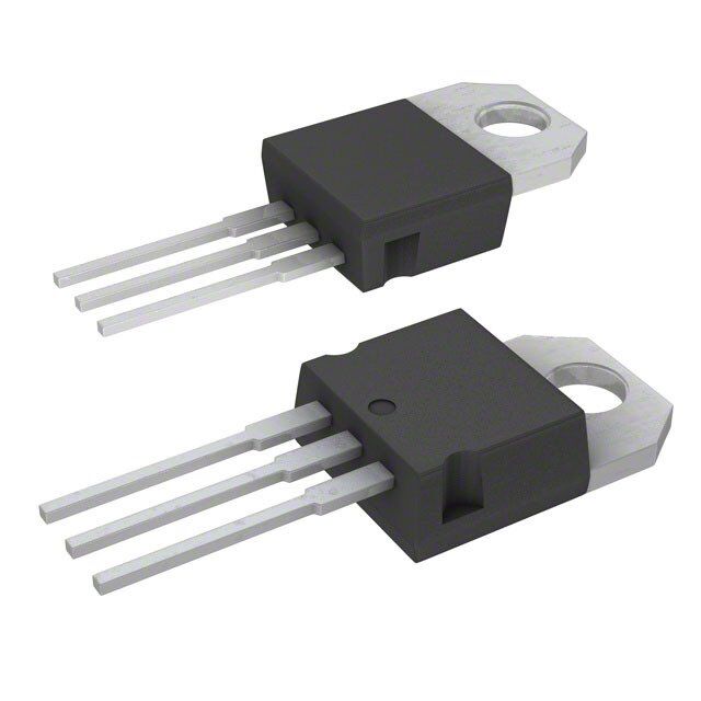
ICGOO电子元器件商城为您提供STPS40SM80CT由STMicroelectronics设计生产,在icgoo商城现货销售,并且可以通过原厂、代理商等渠道进行代购。 STPS40SM80CT价格参考¥8.84-¥8.84。STMicroelectronicsSTPS40SM80CT封装/规格:二极管 - 整流器 - 阵列, Diode Array 1 Pair Common Cathode Schottky 80V 20A Through Hole TO-220-3。您可以下载STPS40SM80CT参考资料、Datasheet数据手册功能说明书,资料中有STPS40SM80CT 详细功能的应用电路图电压和使用方法及教程。
STMicroelectronics(意法半导体)的STPS40SM80CT是一款二极管整流器阵列,属于功率半导体器件。该型号的应用场景主要集中在需要高效、可靠整流功能的电路中,以下是其主要应用场景及特点:

 1. 电源管理
   - 开关电源 (SMPS):STPS40SM80CT可用于开关电源中的整流部分,将交流电转换为直流电,支持高效的电压调节。
   - 逆变器:在逆变器设计中,这款二极管阵列可以用于输出整流或保护电路,确保电流单向流动。

 2. 电机驱动
   - 在电机控制和驱动电路中,该器件可作为续流二极管使用,吸收电机关闭时产生的反向电动势,保护其他敏感元件。
   - 适用于无刷直流电机(BLDC)、步进电机等驱动电路。

 3. 汽车电子
   - 车载充电器:用于汽车电子系统中的充电模块,例如USB充电接口或车载逆变器。
   - 负载突降保护:在汽车环境中,该器件能够承受电压瞬变并提供可靠的整流功能。

 4. 消费类电子产品
   - 适配器与充电器:在手机充电器、笔记本电脑适配器等产品中,STPS40SM80CT可用于输入整流阶段。
   - 家用电器:如冰箱、空调、洗衣机等家电中,该器件可用于电源整流和电机控制。

 5. 工业自动化
   - PLC 和传感器供电:在工业控制系统中,该器件可用于电源整流和信号隔离。
   - 伺服驱动器:为伺服电机提供稳定的电流路径,并保护驱动器免受反向电流损害。

 6. 通信设备
   - 在通信基站、路由器等设备中,该器件可用于电源模块中的整流和保护功能,确保系统的稳定运行。

 技术优势
- 低正向压降:减少功率损耗,提高系统效率。
- 高浪涌能力:能够承受瞬态电流冲击,增强可靠性。
- 紧凑封装:节省PCB空间,适合小型化设计。

总之,STPS40SM80CT凭借其高性能和可靠性,广泛应用于电源管理、电机驱动、汽车电子、消费类电子以及工业自动化等领域,是现代电子系统中不可或缺的整流解决方案之一。
| 参数 | 数值 |
| 产品目录 | |
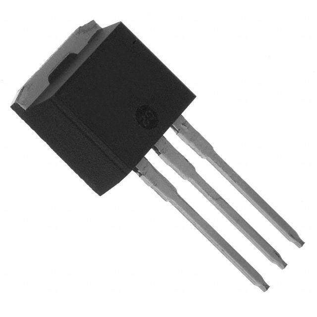
| 描述 | DIODE SCHOTTKY 80V 20A TO220AB肖特基二极管与整流器 Dual Schottky 80V 475mV Vf High Temp |
| 产品分类 | 二极管,整流器 - 阵列分离式半导体 |
| 品牌 | STMicroelectronics |
| 产品手册 | |
| 产品图片 |
|
| rohs | 符合RoHS无铅 / 符合限制有害物质指令(RoHS)规范要求 |
| 产品系列 | 二极管与整流器,肖特基二极管与整流器,STMicroelectronics STPS40SM80CT- |
| 数据手册 | |
| 产品型号 | STPS40SM80CT |
| 不同If时的电压-正向(Vf) | 800mV @ 20A |
| 不同 Vr时的电流-反向漏电流 | 50µA @ 80V |
| 二极管类型 | |
| 二极管配置 | 1 对共阴极 |
| 产品 | Schottky Rectifiers |
| 产品种类 | 肖特基二极管与整流器 |
| 供应商器件封装 | TO-220AB |
| 其它名称 | 497-11363-5 |
| 其它有关文件 | http://www.st.com/web/catalog/sense_power/FM64/CL1571/SC541/SS1618/PF251857?referrer=70071840 |
| 包装 | 管件 |
| 反向恢复时间(trr) | - |
| 商标 | STMicroelectronics |
| 安装类型 | 通孔 |
| 安装风格 | Through Hole |
| 封装 | Tube |
| 封装/外壳 | TO-220-3 |
| 封装/箱体 | TO-220-3 |
| 峰值反向电压 | 80 V |
| 工厂包装数量 | 50 |
| 技术 | Silicon |
| 最大二极管电容 | 45 pF |
| 最大反向漏泄电流 | 50 uA |
| 最大浪涌电流 | 200 A |
| 标准包装 | 50 |
| 正向电压下降 | 0.85 V |
| 正向连续电流 | 30 A |
| 热阻 | 0.88°C/W Jc |
| 电压-DC反向(Vr)(最大值) | 80V |
| 电流-平均整流(Io)(每二极管) | 20A |
| 系列 | STPS40SM80C |
| 速度 | 快速恢复 =< 500 ns,> 200mA(Io) |
| 配置 | Dual |


- 商务部:美国ITC正式对集成电路等产品启动337调查
- 曝三星4nm工艺存在良率问题 高通将骁龙8 Gen1或转产台积电
- 太阳诱电将投资9.5亿元在常州建新厂生产MLCC 预计2023年完工
- 英特尔发布欧洲新工厂建设计划 深化IDM 2.0 战略
- 台积电先进制程称霸业界 有大客户加持明年业绩稳了
- 达到5530亿美元!SIA预计今年全球半导体销售额将创下新高
- 英特尔拟将自动驾驶子公司Mobileye上市 估值或超500亿美元
- 三星加码芯片和SET,合并消费电子和移动部门,撤换高东真等 CEO
- 三星电子宣布重大人事变动 还合并消费电子和移动部门
- 海关总署:前11个月进口集成电路产品价值2.52万亿元 增长14.8%


PDF Datasheet 数据手册内容提取
STPS40SM80C Power Schottky rectifier Features A1 ■ High junction temperature capability K A2 ■ Optimized trade-off between leakage current K K and forward voltage drop ■ Low leakage current A2 ■ Avalanche capability specified A2 ■ Insulated package TO-220FPAB A1 K A1 – insulated voltage: 2000 V I2PAK D2PAK – package capacitance: 45 pF STPS40SM80CR STPS40SM80CG-TR K Description This dual diode Schottky rectifier is suited for high A1 frequency switch mode power supply. A2 K K A2 Packaged in TO-220AB, I2PAK, D2PAK and TO- A1 220FPAB, this device is particularly suited for use TO-220AB TO-220FPAB in notebook, game station, LCD TV and desktop STPS40SM80CT STPS40SM80CFP adapters, providing these applications with a good efficiency at both low and high load. Figure 1. Electrical characteristics(a) T able 1. Device summary I V Symbol Value "Forward" I IF(AV) 2 x 20 A 2 x IO X V 80 V RRM IF T (max) 175 °C j IO X V (typ) 520 mV VRRM F VAR VR V IR VTo VF(Io) VF VF(2xIo) "Reverse" IAR a. V and I must respect the reverse safe ARM ARM operating area defined in Figure13. V and I are AR AR pulse measurements (t < 1 µs). V , I , V and V , p R R RRM F are static characteristics April 2011 Doc ID 018719 Rev 1 1/11 www.st.com 11
Characteristics STPS40SM80C 1 Characteristics T able 2. Absolute ratings (limiting values, per diode, at T = 25 °C unless amb otherwise specified) Symbol Parameter Value Unit V Repetitive peak reverse voltage 80 V RRM I Forward rms current 30 A F(RMS) TO-220AB, T = 145 °C Per diode 20 c IF(AV) Aδv=e 0ra.5ge forward current, I2PAK, D2PAK Tc = 145 °C Per device 40 A TO-220FPAB T = 90 °C Per diode 20 c Surge non repetitive I t = 10 ms sinusoidal T = 25 °C 200 A FSM forward current p c P (1) Repetitive peak avalanche power T = 25 °C, t = 1 µs 9500 W ARM j p Maximum repetitive peak V (2) t < 1 µs, T < 150 °C, I < 28.5 A 100 V ARM avalanche voltage p j AR Maximum single pulse V (2) t < 1 µs, T < 150 °C, I < 28.5 A 100 V ASM peak avalanche voltage p j AR T Storage temperature range -65 to +175 °C stg T Maximum operating junction temperature(3) 175 °C j 1. For temperature or pulse time duration deratings, please refer to figure 3 and 4. More details regarding the avalanche energy measurements and diode validation in the avalanche are provided in the application notes AN1768 and AN2025. 2. See Figure13 dPtot 1 3. < condition to avoid thermal runaway for a diode on its own heatsink dTj Rth(j-a) T able 3. Thermal parameters Symbol Parameter Value Unit TO-220AB per diode 1.60 I2PAK, D2PAK total 0.88 R Junction to case °C/W th(j-c) per diode 4.90 TO-220FPAB total 4.00 TO-220AB 0.15 R Coupling I2PAK, D2PAK °C/W th(c) TO-220FPAB 3.10 When the two diodes 1 and 2 are used simultaneously: ΔT(diode 1) = P(diode 1) x R (Per diode) + P(diode 2) x R j th(j-c) th(c) 2/11 Doc ID 018719 Rev 1
STPS40SM80C Characteristics Table 4. S tatic electrical characteristics (per diode) Symbol Parameter Test conditions Min. Typ. Max. Unit T = 25 °C - 15 50 µA I (1) Reverse leakage current j V = V R R RRM T = 125 °C - 10 30 mA j T = 25 °C - 0.590 0.655 j I = 10 A F T = 125 °C - 0.520 0.560 j T = 25 °C - 0.720 0.800 V (2) Forward voltage drop j I = 20 A V F F T = 125 °C - 0.605 0.690 j T = 25 °C - 0.875 0.985 j I = 40 A F T = 125 °C - 0.725 0.850 j 1. Pulse test: t = 5 ms, δ < 2 % p 2. Pulse test: t = 380 µs, δ < 2 % p To evaluate the conduction losses use the following equation: P = 0.53 x I + 0.008 x I 2 F(AV) F (RMS) Figure 2. A verage forward power dissipation Figure 3. Average forward current versus versus average forward current ambient temperature (per diode) (δ = 0.5, per diode) P (W) I (A) 20 F(AV) 24 F(AV) 18 T δ= 0.5 δ= 1 22 Rth(j-a)= Rth(j-c) 20 16 δ= tp/T tp δ= 0.2 18 14 TO-220AB / I 2PAK / D 2PAK δ= 0.1 16 12 δ= 0.05 14 10 12 TO-220FPAB 8 10 8 6 6 4 4 2 2 0 IF(AV)(A) 0 Tamb(°C) 0 2 4 6 8 10 12 14 16 18 20 22 24 26 0 25 50 75 100 125 150 175 Figure 4. N ormalized avalanche power Figure 5. Normalized avalanche power derating versus pulse duration derating versus junction temperature PARM(tp) PARM(Tj) P (1µs) P (25 °C) 1 ARM 1.2 ARM 1 0.1 0.8 0.6 0.01 0.4 0.2 0.001 tp(µs) 0 Tj(°C) 0.01 0.1 1 10 100 1000 25 50 75 100 125 150 Doc ID 018719 Rev 1 3/11
Characteristics STPS40SM80C Figure 6. Non repetitive surge peak forward Figure 7. Non repetitive surge peak forward current versus overload duration current versus overload duration (maximum values, per diode) (maximum values, per diode) I (A) I (A) 220 M 120 M 200 TO-220AB / I 2PAK / D 2PAK 110 TO-220FPAB 180 100 160 90 140 Tc= 25 °C 7800 Tc= 25 °C 120 100 Tc= 75 °C 60 Tc= 75 °C 50 80 Tc= 125 °C 40 Tc= 125 °C 60 30 40 IM 20 IM 20 δ= 0t.5 t(s) 10 δ= 0t.5 t(s) 0 0 1.E-03 1.E-02 1.E-01 1.E+00 1.E-03 1.E-02 1.E-01 1.E+00 Figure 8. Relative thermal impedance Figure 9. Relative thermal impedance junction to case versus pulse junction to case versus pulse duration duration (TO-220FPAB) Z /R Z /R 1.0 th(j-c) th(j-c) 1.0 th(j-c) th(j-c) TO-220AB / I 2PAK / D 2PAK TO-220FPAB 0.9 0.9 0.8 0.8 0.7 0.7 0.6 0.6 0.5 0.5 0.4 0.4 0.3 0.3 Single pulse 0.2 Single pulse 0.2 0.1 0.1 0.0 tp(s) 0.0 tp(s) 1.E-04 1.E-03 1.E-02 1.E-01 1.E+00 1.E-03 1.E-02 1.E-01 1.E+00 1.E+01 Figure 10. Reverse leakage current versus Figure 11. Junction capacitance versus reverse voltage applied reverse voltage applied (typical values, per diode) (typical values, per diode) I (µA) C(pF) 1.E+05 R 10000 F = 1 MHz Tj= 150 °C Vosc= 30 mVRMS 1.E+04 Tj= 25 °C T= 125 °C j T= 100 °C 1.E+03 j T= 75 °C 1000 j 1.E+02 T= 50 °C j 1.E+01 T= 25 °C j V (V) V (V) 1.E+00 R 100 R 0 10 20 30 40 50 60 70 80 1 10 100 4/11 Doc ID 018719 Rev 1
STPS40SM80C Characteristics Figure 12. Forward voltage drop versus Figure 13. Reverse safe operating area forward current (per diode) (t < 1 µs and T < 150 °C) p j 40 IFM(A) 29.0 Iarm(A) I (V ) 150 °C,1µs 35 Tj= 125 °C 28.0 arm arm (Maximum values) 27.0 30 26.0 25 25.0 T= 125 °C j 20 (Typical values) 24.0 23.0 15 22.0 10 Tj= 25 °C 21.0 (Maximum values) 5 20.0 V (V) 0 VFM(V) 19.0 arm 0.0 0.1 0.2 0.3 0.4 0.5 0.6 0.7 0.8 0.9 1.0 100 105 110 115 120 125 130 135 140 145 150 Figure 14. Thermal resistance junction to ambient versus copper surface under tab for D2PAK R (°C/W) 80 th(j-a) epoxy printed board copper thickness = 35 µm 70 60 D2PAK 50 40 30 20 10 S (cm2) 0 Cu 0 5 10 15 20 25 30 35 40 Doc ID 018719 Rev 1 5/11
Package information STPS40SM80C 2 Package information ● Epoxy meets UL94, V0 ● Cooling method: by conduction (C) ● Recommended torque value: 0.4 to 0.6 N·m In order to meet environmental requirements, ST offers these devices in different grades of ECOPACK® packages, depending on their level of environmental compliance. ECOPACK® specifications, grade definitions and product status are available at: www.st.com. ECOPACK® is an ST trademark. T able 5. TO-220AB dimensions Dimensions Ref. Millimeters Inches Min. Max. Min. Max. A 4.40 4.60 0.173 0.181 C 1.23 1.32 0.048 0.051 H2 A D 2.40 2.72 0.094 0.107 Dia C E 0.49 0.70 0.019 0.027 L5 L7 F 0.61 0.88 0.024 0.034 F1 1.14 1.70 0.044 0.066 L6 F2 1.14 1.70 0.044 0.066 L2 F2 G 4.95 5.15 0.194 0.202 F1 L9 D G1 2.40 2.70 0.094 0.106 H2 10 10.40 0.393 0.409 L4 F L2 16.4 Typ. 0.645 Typ. M L4 13 14 0.511 0.551 G1 E L5 2.65 2.95 0.104 0.116 G L6 15.25 15.75 0.600 0.620 L7 6.20 6.60 0.244 0.259 L9 3.50 3.93 0.137 0.154 M 2.6 Typ. 0.102 Typ. Dia. 3.75 3.85 0.147 0.151 6/11 Doc ID 018719 Rev 1
STPS40SM80C Package information Table 6. TO-220FPAB dimensions Dimensions Ref. Millimeters Inches Min. Max. Min. Max. A 4.4 4.9 0.173 0.192 A B 2.5 2.9 0.098 0.114 H B D 2.45 2.75 0.096 0.108 E 0.4 0.7 0.016 0.028 Dia. F 0.6 1 0.024 0.039 L6 F1 1.15 1.7 0.045 0.067 L7 L2 F2 1.15 1.7 0.045 0.067 L3 G 4.95 5.2 0.195 0.205 G1 2.4 2.7 0.094 0.106 F1 F2 L4 D H 10 10.7 0.394 0.421 L2 16 Typ. 0.630 Typ. F E G1 L3 28.6 30.6 1.126 1.205 L4 9.8 10.7 0.386 0.421 G L6 15.8 16.4 0.622 0.646 L7 9 9.9 0.354 0.390 Dia. 2.9 3.5 0.114 0.138 Doc ID 018719 Rev 1 7/11
Package information STPS40SM80C T able 7. D2PAK dimensions Dimensions Ref. Millimeters Inches Min. Max. Min. Max. A 4.40 4.60 0.173 0.181 A A1 2.49 2.69 0.098 0.106 E C2 L2 A2 0.03 0.23 0.001 0.009 B 0.70 0.93 0.027 0.037 D B2 1.14 1.70 0.045 0.067 L C 0.45 0.60 0.017 0.024 L3 A1 C2 1.23 1.36 0.048 0.054 B2 C R D 8.95 9.35 0.352 0.368 B E 10.00 10.40 0.393 0.409 G G 4.88 5.28 0.192 0.208 A2 L 15.00 15.85 0.590 0.624 M * L2 1.27 1.40 0.050 0.055 V2 L3 1.40 1.75 0.055 0.069 * FLAT ZONE NO LESSTHAN 2mm M 2.40 3.20 0.094 0.126 R 0.40 typ. 0.016 typ. V2 0° 8° 0° 8° Figure 15. D2PAK footprint (dimensions in mm) 16.90 10.30 5.08 1.30 3.70 8.90 8/11 Doc ID 018719 Rev 1
STPS40SM80C Package information T able 8. I2PAK dimensions Dimensions Ref. Millimeters Inches Min. Max. Min. Max. A A 4.40 4.60 0.173 0.181 E c2 A1 2.40 2.72 0.094 0.107 L2 b 0.61 0.88 0.024 0.035 b1 1.14 1.70 0.044 0.067 D c 0.49 0.70 0.019 0.028 L1 A1 c2 1.23 1.32 0.048 0.052 D 8.95 9.35 0.352 0.368 b1 L e 2.40 2.70 0.094 0.106 e1 4.95 5.15 0.195 0.203 b c E 10 10.40 0.394 0.409 e e1 L 13 14 0.512 0.551 L1 3.50 3.93 0.138 0.155 L2 1.27 1.40 0.050 0.055 Doc ID 018719 Rev 1 9/11
Ordering information STPS40SM80C 3 Ordering information T able 9. Ordering information Order code Marking Package Weight Base qty Delivery mode STPS40SM80CT PS40SM80CT TO-220AB 1.9 g 50 Tube STPS40SM80CFP PS40SM80CFP TO-220FPAB 2.0 g 50 Tube STPS40SM80CR PS40SM80CR I2PAK 1.49 g 50 Tube STPS40SM80CG-TR PS40SM80CG D2PAK 1.48 g 1000 Tape and reel 4 Revision history T able 10. Revision history Date Revision Changes 11-Apr-2011 1 First issue. 10/11 Doc ID 018719 Rev 1
STPS40SM80C Please Read Carefully: Information in this document is provided solely in connection with ST products. STMicroelectronics NV and its subsidiaries (“ST”) reserve the right to make changes, corrections, modifications or improvements, to this document, and the products and services described herein at any time, without notice. All ST products are sold pursuant to ST’s terms and conditions of sale. Purchasers are solely responsible for the choice, selection and use of the ST products and services described herein, and ST assumes no liability whatsoever relating to the choice, selection or use of the ST products and services described herein. No license, express or implied, by estoppel or otherwise, to any intellectual property rights is granted under this document. If any part of this document refers to any third party products or services it shall not be deemed a license grant by ST for the use of such third party products or services, or any intellectual property contained therein or considered as a warranty covering the use in any manner whatsoever of such third party products or services or any intellectual property contained therein. UNLESS OTHERWISE SET FORTH IN ST’S TERMS AND CONDITIONS OF SALE ST DISCLAIMS ANY EXPRESS OR IMPLIED WARRANTY WITH RESPECT TO THE USE AND/OR SALE OF ST PRODUCTS INCLUDING WITHOUT LIMITATION IMPLIED WARRANTIES OF MERCHANTABILITY, FITNESS FOR A PARTICULAR PURPOSE (AND THEIR EQUIVALENTS UNDER THE LAWS OF ANY JURISDICTION), OR INFRINGEMENT OF ANY PATENT, COPYRIGHT OR OTHER INTELLECTUAL PROPERTY RIGHT. UNLESS EXPRESSLY APPROVED IN WRITING BY AN AUTHORIZED ST REPRESENTATIVE, ST PRODUCTS ARE NOT RECOMMENDED, AUTHORIZED OR WARRANTED FOR USE IN MILITARY, AIR CRAFT, SPACE, LIFE SAVING, OR LIFE SUSTAINING APPLICATIONS, NOR IN PRODUCTS OR SYSTEMS WHERE FAILURE OR MALFUNCTION MAY RESULT IN PERSONAL INJURY, DEATH, OR SEVERE PROPERTY OR ENVIRONMENTAL DAMAGE. ST PRODUCTS WHICH ARE NOT SPECIFIED AS "AUTOMOTIVE GRADE" MAY ONLY BE USED IN AUTOMOTIVE APPLICATIONS AT USER’S OWN RISK. Resale of ST products with provisions different from the statements and/or technical features set forth in this document shall immediately void any warranty granted by ST for the ST product or service described herein and shall not create or extend in any manner whatsoever, any liability of ST. ST and the ST logo are trademarks or registered trademarks of ST in various countries. Information in this document supersedes and replaces all information previously supplied. The ST logo is a registered trademark of STMicroelectronics. All other names are the property of their respective owners. © 2011 STMicroelectronics - All rights reserved STMicroelectronics group of companies Australia - Belgium - Brazil - Canada - China - Czech Republic - Finland - France - Germany - Hong Kong - India - Israel - Italy - Japan - Malaysia - Malta - Morocco - Philippines - Singapore - Spain - Sweden - Switzerland - United Kingdom - United States of America www.st.com Doc ID 018719 Rev 1 11/11