ICGOO在线商城 > STPS3030CR
 Datasheet下载
- 型号: STPS3030CR
- 制造商: STMicroelectronics
- 库位|库存: xxxx|xxxx
- 要求:
| 数量阶梯 | 香港交货 | 国内含税 |
| +xxxx | $xxxx | ¥xxxx |
查看当月历史价格
查看今年历史价格
STPS3030CR产品简介:
ICGOO电子元器件商城为您提供STPS3030CR由STMicroelectronics设计生产,在icgoo商城现货销售,并且可以通过原厂、代理商等渠道进行代购。 提供STPS3030CR价格参考以及STMicroelectronicsSTPS3030CR封装/规格参数等产品信息。 你可以下载STPS3030CR参考资料、Datasheet数据手册功能说明书, 资料中有STPS3030CR详细功能的应用电路图电压和使用方法及教程。
| 参数 | 数值 |
| 产品目录 | |
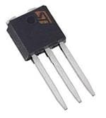
| 描述 | DIODE SCHOTTKY 30V 15A I2PAK肖特基二极管与整流器 LD PWR SCHOT |
| 产品分类 | 二极管,整流器 - 阵列分离式半导体 |
| 品牌 | STMicroelectronics |
| 产品手册 | |
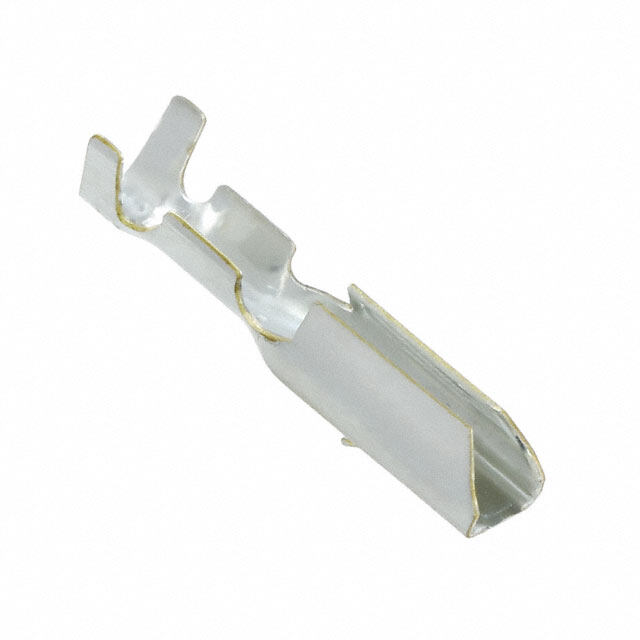
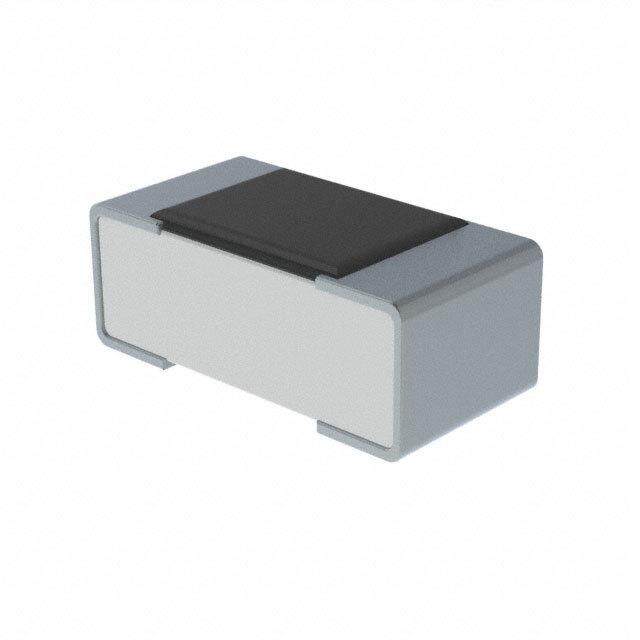
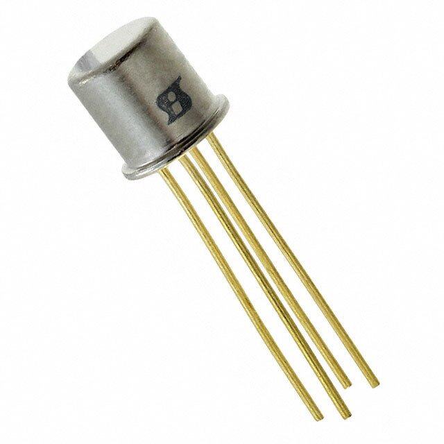
| 产品图片 |
|
| rohs | 符合RoHS无铅 / 符合限制有害物质指令(RoHS)规范要求 |
| 产品系列 | 二极管与整流器,肖特基二极管与整流器,STMicroelectronics STPS3030CR- |
| 数据手册 | |
| 产品型号 | STPS3030CR |
| 不同If时的电压-正向(Vf) | 490mV @ 15A |
| 不同 Vr时的电流-反向漏电流 | 1mA @ 30V |
| 二极管类型 | |
| 二极管配置 | 1 对共阴极 |
| 产品 | Schottky Rectifiers |
| 产品种类 | 肖特基二极管与整流器 |
| 供应商器件封装 | I2PAK |
| 其它名称 | 497-12648-5 |
| 其它有关文件 | http://www.st.com/web/catalog/sense_power/FM64/CL1571/SC541/SS1618/PF64878?referrer=70071840 |
| 包装 | 管件 |
| 反向恢复时间(trr) | - |
| 商标 | STMicroelectronics |
| 安装类型 | 通孔 |
| 安装风格 | SMD/SMT |
| 封装 | Tube |
| 封装/外壳 | TO-262-3,长引线,I²Pak,TO-262AA |
| 封装/箱体 | I2PAK |
| 峰值反向电压 | 30 V |
| 工作温度范围 | + 150 C |
| 工厂包装数量 | 50 |
| 技术 | Silicon |
| 最大反向漏泄电流 | 1000 uA |
| 最大工作温度 | + 150 C |
| 最大浪涌电流 | 250 A |
| 最小工作温度 | - 65 C |
| 标准包装 | 50 |
| 正向电压下降 | 0.58 V |
| 正向连续电流 | 30 A |
| 热阻 | 0.8°C/W Jc |
| 电压-DC反向(Vr)(最大值) | 30V |
| 电流-平均整流(Io)(每二极管) | 15A |
| 系列 | STPS3030C |
| 速度 | 快速恢复 =< 500 ns,> 200mA(Io) |
| 配置 | Dual Common Cathode |


- 商务部:美国ITC正式对集成电路等产品启动337调查
- 曝三星4nm工艺存在良率问题 高通将骁龙8 Gen1或转产台积电
- 太阳诱电将投资9.5亿元在常州建新厂生产MLCC 预计2023年完工
- 英特尔发布欧洲新工厂建设计划 深化IDM 2.0 战略
- 台积电先进制程称霸业界 有大客户加持明年业绩稳了
- 达到5530亿美元!SIA预计今年全球半导体销售额将创下新高
- 英特尔拟将自动驾驶子公司Mobileye上市 估值或超500亿美元
- 三星加码芯片和SET,合并消费电子和移动部门,撤换高东真等 CEO
- 三星电子宣布重大人事变动 还合并消费电子和移动部门
- 海关总署:前11个月进口集成电路产品价值2.52万亿元 增长14.8%

PDF Datasheet 数据手册内容提取
STPS3030/CT/CG/CR Low drop power Schottky rectifier Main product characteristics A1 I 2 x 15 A K F(AV) VRRM 30 V A2 T (max) 150° C j K V (max) 0.42 V F Features and benefits ■ Very small conduction losses A2 A2 ■ Negligible switching losses A1 A1K ■ Extremely fast switching D2PAK TO-220AB ■ Low forward voltage drop for higher efficiency STPS3030CG STPS3030CT ■ Low thermal resistance ■ Avalanche capability specified Description Dual Schottky rectifier suited for switch mode A2 power supply and high frequency DC to DC K converters. A1 I2PAK Packaged in TO-220AB, D2PAK and I2PAK, this STPS3030CR device is intended for use in low voltage high frequency inverters, free-wheeling and polarity j protection applications. October 2006 Rev 4 1/9 www.st.com 9
Characteristics STPS3030CT/CG/CR 1 Characteristics T able 1. Absolute ratings (limiting values, per diode) Symbol Parameter Value Unit V Repetitive peak reverse voltage 30 V RRM I RMS forward current 30 A F(RMS) T = 135° C Per diode 15 c I Average forward current A F(AV) δ = 0.5 Per device 30 I Surge non repetitive forward current t = 10 ms sinusoidal 250 A FSM p I Peak repetitive reverse current t = 2 µs square F= 1 kHz 1 A RRM p I Non repetitive peak reverse current t = 100 µs square 3 A RSM p P Repetitive peak avalanche power t = 1 µs T = 25° C 4100 W ARM p j T Storage temperature range -65 to + 150 °C stg T Maximum operating junction temperature (1) 150 °C j dV/dt Critical rate of rise of reverse voltage (rated V , T = 25° C) 10000 V/µs R j 1. d----dP----T-t--o-j---t<R-----t--h----(-1--j--–-----a----)- condition to avoid thermal runaway for a diode on its own heatsink T able 2. Thermal resistance Symbol Parameter Value Unit Per diode 1.2 R Junction to case TO-220AB - D2PAK - I2PAK th(j-c) Total 0.8 °C/W R Coupling 0.4 th(c) T able 3. Static electrical characteristics (per diode) Symbol Parameter Test conditions Min. Typ. Max. Unit T = 25° C 0.23 1.0 I (1) Reverse leakage current j V = V mA R R RRM T = 125° C 125 180 j T = 25° C I = 15 A 0.44 0.49 j F T = 125° C I = 15 A 0.36 0.40 V (1) Forward voltage drop j F V F T = 25° C I = 30 A 0.53 0.58 j F T = 125° C I = 30 A 0.49 0.53 j F 1. Pulse test: tp = 380 µs, δ < 2% To evaluate the conduction losses use the following equation: P = 0.26 x I + 0.0107 I 2 F(AV) F (RMS) 2/9
STPS3030CT/CG/CR Characteristics Figure 1. C onduction losses versus average Figure 2. Average forward current versus current ambient temperature (δ = 0.5) P(W) IF(av)(A) 10 18 δ= 0.1 δ= 0.2 δ= 0.5 9 δ= 0.05 16 Rth(j-a)=Rth(j-c) 8 14 7 δ= 1 12 6 10 5 8 4 6 Rth(j-a)=50°C/W 3 2 T 4 1 IF(av)(A) δ=tp/T tp 2 Tamb(°C) 0 0 0 2 4 6 8 10 12 14 16 18 20 0 25 50 75 100 125 150 Figure 3. N ormalized avalanche power Figure 4. Normalized avalanche power derating versus pulse duration derating versus junction temperature PARM(tp) PARM(tp) PARM(1µs) PARM(25°C) 1 1.2 1 0.1 0.8 0.6 0.01 0.4 0.2 tp(µs) Tj(°C) 0.001 0 0.01 0.1 1 10 100 1000 0 25 50 75 100 125 150 Figure 5. N on repetitive surge peak forward Figure 6. Relative variation of thermal current versus overload duration impedance junction to case versus (maximum values) pulse duration IM(A) Zth(j-c)/Rth(j-c) 250 1.0 225 0.9 200 0.8 175 0.7 150 0.6 δ= 0.5 125 TC=25°C 0.5 100 TC=75°C 0.4 δ= 0.2 75 0.3 δ= 0.1 50 TC=125°C 0.2 T Single pulse 25 t(s) 0.1 tp(s) δ=tp/T tp 0 0.0 1.E-03 1.E-02 1.E-01 1.E+00 1.E-03 1.E-02 1.E-01 1.E+00 3/9
Characteristics STPS3030CT/CG/CR Figure 7. R everse leakage current versus Figure 8. Junction capacitance versus reverse voltage applied (typical reverse voltage applied (typical values) values) IR(mA) C(nF) 1.E+03 10.0 1.E+02 Tj=150°C VFoTs=jc==123M50°HmCzV Tj=125°C 1.E+01 Tj=100°C Tj=75°C 1.0 1.E+00 Tj=50°C 1.E-01 Tj=25°C VR(V) VR(V) 1.E-02 0.1 0 5 10 15 20 25 30 1 10 100 Figure 9. F orward voltage drop versus Figure 10. Thermal resistance junction to forward current ambient versus copper surface under tab (epoxy printed board FR4, Cu = 35 µm) IFM(A) Rth(j-a)(°C/W) 100 80 D²PAK 70 ((MMaaxxTTiimmjj==uu11mm2255 vv°°aaCClluueess)) 60 ((TTyyppTTiijjcc==aa11ll22vv55aa°°llCCuueess)) 50 10 (MaxiTmj=u2m5 °vCalues) 40 30 20 VFM(V) 10 S(cm²) 1 0 0.0 0.2 0.4 0.6 0.8 1.0 1.2 0 5 10 15 20 25 30 35 40 4/9
STPS3030CT/CG/CR Package information 2 Package information ● Epoxy meets UL94,V0 ● Cooling method: C ● Recommended torque value: 0.55 Nm ● Maximum torque value: 0.70 Nm T able 4. I2PAK dimensions Dimensions Ref. Millimeters Inches Min. Max. Min. Max. A A 4.40 4.60 0.173 0.181 E c2 A1 2.40 2.72 0.094 0.107 L2 b 0.61 0.88 0.024 0.035 b1 1.14 1.70 0.044 0.067 D c 0.49 0.70 0.019 0.028 c2 1.23 1.32 0.048 0.052 L1 A1 D 8.95 9.35 0.352 0.368 e 2.40 2.70 0.094 0.106 b1 L e1 4.95 5.15 0.195 0.203 E 10 10.40 0.394 0.409 b c L 13 14 0.512 0.551 e L1 3.50 3.93 0.138 0.155 e1 L2 1.27 1.40 0.050 0.055 5/9
Package information STPS3030CT/CG/CR Table 5. D2PAK dimensions Dimensions Ref Millimeters Inches Min. Max. Min. Max. A 4.40 4.60 0.173 0.181 A A1 2.49 2.69 0.098 0.106 E C2 L2 A2 0.03 0.23 0.001 0.009 B 0.70 0.93 0.027 0.037 D L B2 1.14 1.70 0.045 0.067 L3 C 0.45 0.60 0.017 0.024 A1 C2 1.23 1.36 0.048 0.054 B2 C R B D 8.95 9.35 0.352 0.368 G E 10.00 10.40 0.393 0.409 A2 G 4.88 5.28 0.192 0.208 L 15.00 15.85 0.590 0.624 M * L2 1.27 1.40 0.050 0.055 V2 L3 1.40 1.75 0.055 0.069 * FLAT ZONE NO LESSTHAN 2mm M 2.40 3.20 0.094 0.126 R 0.40 typ. 0.016 typ. V2 0° 8° 0° 8° Figure 11. Footprint (dimensions in millimeters) 16.90 10.30 5.08 1.30 3.70 8.90 6/9
STPS3030CT/CG/CR Package information T able 6. TO-220AB dimensions Dimensions Ref Millimeters Inches Min. Max. Min. Max. A 4.40 4.60 0.173 0.181 C 1.23 1.32 0.048 0.051 D 2.40 2.72 0.094 0.107 H2 A Dia C E 0.49 0.70 0.019 0.027 L5 F 0.61 0.88 0.024 0.034 L7 F1 1.14 1.70 0.044 0.066 L6 F2 1.14 1.70 0.044 0.066 L2 F2 G 4.95 5.15 0.194 0.202 F1 L9 D G1 2.40 2.70 0.094 0.106 L4 H2 10 10.40 0.393 0.409 F M L2 16.4 typ. 0.645 typ. G1 E L4 13 14 0.511 0.551 G L5 2.65 2.95 0.104 0.116 L6 15.25 15.75 0.600 0.620 L7 6.20 6.60 0.244 0.259 L9 3.50 3.93 0.137 0.154 M 2.6 typ. 0.102 typ. Diam 3.75 3.85 0.147 0.151 In order to meet environmental requirements, ST offers these devices in ECOPACK® packages. These packages have a lead-free second level interconnect. The category of second level interconnect is marked on the package and on the inner box label, in compliance with JEDEC Standard JESD97. The maximum ratings related to soldering conditions are also marked on the inner box label. ECOPACK is an ST trademark. ECOPACK specifications are available at: www.st.com. 7/9
Ordering information STPS3030CT/CG/CR 3 Ordering information Delivery Ordering type Marking Package Weight Base qty mode STPS3030CT STPS3030CT TO-220AB 2.2 g 50 Tube STPS3030CG STPS3030CG D2PAK 1.48 g 50 Tube STPS3030CG-TR STPS3030CG D2PAK 1.48 g 1000 Tape and reel STPS3030CR STPS3030CR I2PAK 1.49 g 50 Tube 4 Revision history Date Revision Changes Jul-2006 3A Initial release. Reformatted to current standards. Corrected dimensions for I2PAK in 16-Oct-2006 4 Table 4 8/9
STPS3030CT/CG/CR Please Read Carefully: Information in this document is provided solely in connection with ST products. STMicroelectronics NV and its subsidiaries (“ST”) reserve the right to make changes, corrections, modifications or improvements, to this document, and the products and services described herein at any time, without notice. All ST products are sold pursuant to ST’s terms and conditions of sale. Purchasers are solely responsible for the choice, selection and use of the ST products and services described herein, and ST assumes no liability whatsoever relating to the choice, selection or use of the ST products and services described herein. No license, express or implied, by estoppel or otherwise, to any intellectual property rights is granted under this document. If any part of this document refers to any third party products or services it shall not be deemed a license grant by ST for the use of such third party products or services, or any intellectual property contained therein or considered as a warranty covering the use in any manner whatsoever of such third party products or services or any intellectual property contained therein. UNLESS OTHERWISE SET FORTH IN ST’S TERMS AND CONDITIONS OF SALE ST DISCLAIMS ANY EXPRESS OR IMPLIED WARRANTY WITH RESPECT TO THE USE AND/OR SALE OF ST PRODUCTS INCLUDING WITHOUT LIMITATION IMPLIED WARRANTIES OF MERCHANTABILITY, FITNESS FOR A PARTICULAR PURPOSE (AND THEIR EQUIVALENTS UNDER THE LAWS OF ANY JURISDICTION), OR INFRINGEMENT OF ANY PATENT, COPYRIGHT OR OTHER INTELLECTUAL PROPERTY RIGHT. UNLESS EXPRESSLY APPROVED IN WRITING BY AN AUTHORIZED ST REPRESENTATIVE, ST PRODUCTS ARE NOT RECOMMENDED, AUTHORIZED OR WARRANTED FOR USE IN MILITARY, AIR CRAFT, SPACE, LIFE SAVING, OR LIFE SUSTAINING APPLICATIONS, NOR IN PRODUCTS OR SYSTEMS WHERE FAILURE OR MALFUNCTION MAY RESULT IN PERSONAL INJURY, DEATH, OR SEVERE PROPERTY OR ENVIRONMENTAL DAMAGE. ST PRODUCTS WHICH ARE NOT SPECIFIED AS "AUTOMOTIVE GRADE" MAY ONLY BE USED IN AUTOMOTIVE APPLICATIONS AT USER’S OWN RISK. Resale of ST products with provisions different from the statements and/or technical features set forth in this document shall immediately void any warranty granted by ST for the ST product or service described herein and shall not create or extend in any manner whatsoever, any liability of ST. ST and the ST logo are trademarks or registered trademarks of ST in various countries. Information in this document supersedes and replaces all information previously supplied. The ST logo is a registered trademark of STMicroelectronics. All other names are the property of their respective owners. © 2006 STMicroelectronics - All rights reserved STMicroelectronics group of companies Australia - Belgium - Brazil - Canada - China - Czech Republic - Finland - France - Germany - Hong Kong - India - Israel - Italy - Japan - Malaysia - Malta - Morocco - Singapore - Spain - Sweden - Switzerland - United Kingdom - United States of America www.st.com 9/9