ICGOO在线商城 > 分立半导体产品 > 晶体管 - FET,MOSFET - 单 > STN4NF06L

 Datasheet下载
- 型号: STN4NF06L
- 制造商: STMicroelectronics
- 库位|库存: xxxx|xxxx
- 要求:
| 数量阶梯 | 香港交货 | 国内含税 |
| +xxxx | $xxxx | ¥xxxx |
查看当月历史价格
查看今年历史价格
STN4NF06L产品简介:
ICGOO电子元器件商城为您提供STN4NF06L由STMicroelectronics设计生产,在icgoo商城现货销售,并且可以通过原厂、代理商等渠道进行代购。 STN4NF06L价格参考。STMicroelectronicsSTN4NF06L封装/规格:晶体管 - FET,MOSFET - 单, 表面贴装 N 沟道 60V 4A(Tc) 3.3W(Tc) SOT-223。您可以下载STN4NF06L参考资料、Datasheet数据手册功能说明书,资料中有STN4NF06L 详细功能的应用电路图电压和使用方法及教程。
| 参数 | 数值 |
| 产品目录 | |
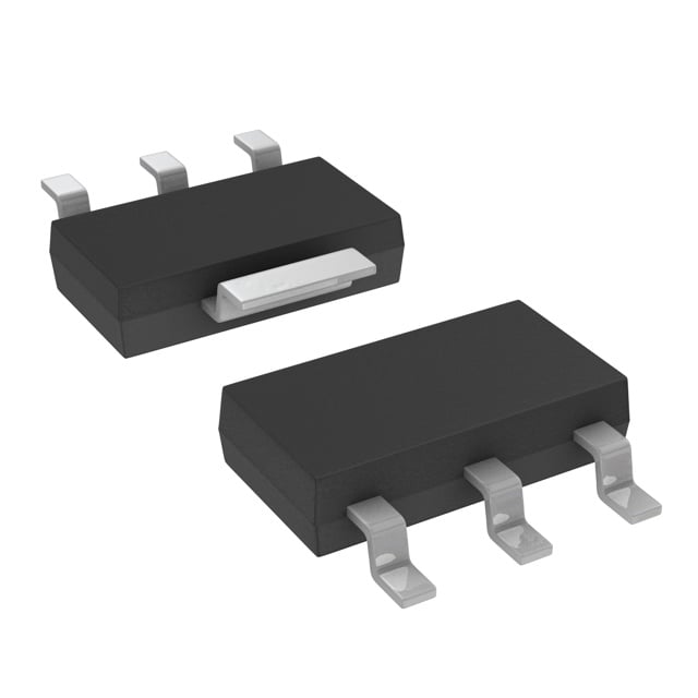
| 描述 | MOSFET N-CH 60V 4A SOT-223 |
| 产品分类 | FET - 单 |
| FET功能 | 逻辑电平门 |
| FET类型 | MOSFET N 通道,金属氧化物 |
| 品牌 | STMicroelectronics |
| 数据手册 | |
| 产品图片 |
|
| 产品型号 | STN4NF06L |
| rohs | 无铅 / 符合限制有害物质指令(RoHS)规范要求 |
| 产品系列 | STripFET™ II |
| 不同Id时的Vgs(th)(最大值) | 2.8V @ 250µA |
| 不同Vds时的输入电容(Ciss) | 340pF @ 25V |
| 不同Vgs时的栅极电荷(Qg) | 9nC @ 5V |
| 不同 Id、Vgs时的 RdsOn(最大值) | 100 毫欧 @ 1.5A,10V |
| 产品培训模块 | http://www.digikey.cn/PTM/IndividualPTM.page?site=cn&lang=zhs&ptm=26067 |
| 产品目录页面 | |
| 供应商器件封装 | SOT-223 |
| 其它名称 | 497-10315-1 |
| 其它有关文件 | http://www.st.com/web/catalog/sense_power/FM100/CL824/SC1165/PF185329?referrer=70071840 |
| 功率-最大值 | 3.3W |
| 包装 | 剪切带 (CT) |
| 安装类型 | 表面贴装 |
| 封装/外壳 | TO-261-4,TO-261AA |
| 标准包装 | 1 |
| 漏源极电压(Vdss) | 60V |
| 电流-连续漏极(Id)(25°C时) | 4A (Tc) |


- 商务部:美国ITC正式对集成电路等产品启动337调查
- 曝三星4nm工艺存在良率问题 高通将骁龙8 Gen1或转产台积电
- 太阳诱电将投资9.5亿元在常州建新厂生产MLCC 预计2023年完工
- 英特尔发布欧洲新工厂建设计划 深化IDM 2.0 战略
- 台积电先进制程称霸业界 有大客户加持明年业绩稳了
- 达到5530亿美元!SIA预计今年全球半导体销售额将创下新高
- 英特尔拟将自动驾驶子公司Mobileye上市 估值或超500亿美元
- 三星加码芯片和SET,合并消费电子和移动部门,撤换高东真等 CEO
- 三星电子宣布重大人事变动 还合并消费电子和移动部门
- 海关总署:前11个月进口集成电路产品价值2.52万亿元 增长14.8%


PDF Datasheet 数据手册内容提取
STN4NF06L Datasheet Automotive-grade N-channel 60 V, 0.07 Ω typ., 4 A STripFET II Power MOSFET in a SOT-223 package Features 4 Order code VDS RDS(on) max. ID STN4NF06L 60 V < 0.1 Ω 4 A 3 2 1 • AEC-Q101 qualified SOT-223 • Exceptional dv/dt capability • 100% avalanche tested • Low gate charge D(2, 4) Applications • Switching applications G(1) Description This Power MOSFET has been developed using STMicroelectronics' unique S(3) STripFET process, which is specifically designed to minimize input capacitance and Int_schem_nTnZ_SOT_223 gate charge. This renders the device suitable for use as primary switch in advanced high-efficiency isolated DC-DC converters for telecom and computer applications, and applications with low gate charge driving requirements. Product status link STN4NF06L Product summary Order code STN4NF06L Marking 4NF06L Package SOT-223 Packing Tape and reel DS5801 - Rev 3 - May 2020 www.st.com For further information contact your local STMicroelectronics sales office.
STN4NF06L Electrical ratings 1 Electrical ratings Table 1. Absolute maximum ratings Symbol Parameter Value Unit VDS Drain-source voltage (VGS = 0 V) 60 V VGS Gate-source voltage ±16 V Drain current (continuous) at TC = 25 °C 4 A ID(1) Drain current (continuous) at TC = 100 °C 2.9 A IDM(2) Drain current (pulsed) 16 A PTOT Total power dissipation at TC = 25 °C 3.3 W Derating Factor 0.026 W/°C dv/dt(3) Peak diode recovery avalanche energy 10 V/ns EAS(4) Single pulse avalanche energy 200 mJ Tstg Storage temperature range -55 to 150 °C TJ Operating junction temperature range 1. Current limited by the package. 2. Pulse width limited by safe operating area. 3. ISD ≤ 3 A, di/dt ≤ 150 A/μs, VDD = V(BR)DSS, TJ ≤ TJ max. 4. Starting TJ = 25 °C, ID = 4 A, VDD = 30 V. Table 2. Thermal data Symbol Parameter Value Unit Rthj-pcb (1) 38 °C/W Thermal resistance junction-pcb Rthj-pcb(2) 100 °C/W TJ(3) Maximum lead temperature for soldering purpose 260 °C 1. When Mounted on FR-4 board with 1 inch2 pad, 2 oz. of Cu. and t <10 s. 2. When mounted on minimum recommended footprint. 3. For 10 s 1.6 mm from case. DS5801 - Rev 3 page 2/14
STN4NF06L Electrical characteristics 2 Electrical characteristics T = 25 °C unless otherwise specified C Table 3. On-/off-states Symbol Parameter Test conditions Min. Typ. Max. Unit V(BR)DSS Drain-source breakdown voltage VGS = 0 V, ID = 250 μA 60 V VGS = 0 V, VDS = 60 V 1 µA IDSS Zero gate voltage drain current VGS = 0 V, VDS = 60 V, TC = 125 °C 10 µA IGSS Gate-body leakage current VDS = 0 V, VGS = ±16 V ±100 nA VGS(th) Gate threshold voltage VDS = VGS, ID = 250 µA 1 2.8 V VGS = 10 V, ID = 1.5 A 0.07 0.10 RDS(on) Static drain-source on-resistance Ω VGS = 5 V, ID = 1.5 A 0.085 0.12 Table 4. Dynamic Symbol Parameter Test conditions Min. Typ. Max. Unit Ciss Input capacitance - 340 pF Coss Output capacitance VDS = 25 V, f = 1 MHz, VGS = 0 V - 63 pF Crss Reverse transfer capacitance - 30 pF Qg Total gate charge VDD = 48 V, ID = 3 A - 7 9 nC Qgs Gate-source charge RG = 4.7 Ω, VGS = 5 V - 1.5 nC (see Figure 14. Test circuit for gate Qgd Gate-drain charge charge behavior) - 2.8 nC Table 5. Switching times Symbol Parameter Test conditions Min. Typ. Max. Unit td(on) Turn-on delay time VDD = 30 V, ID = 1.5 A, - 9 - ns tr Rise time RG = 4.7 Ω, VGS = 5 V - 25 - ns td(off) Turn-off delay time (see Figure 13. Test circuit for resistive - 20 - ns load switching times and tf Fall time Figure 18. Switching time waveform) - 10 - ns DS5801 - Rev 3 page 3/14
STN4NF06L Electrical characteristics Table 6. Source-drain diode Symbol Parameter Test conditions Min. Typ. Max. Unit ISD Source-drain current - 4 A ISDM(1) Source-drain current (pulsed) - 16 A VSD(2) Forward on voltage ISD = 4 A, VGS = 0 V - 1.5 V trr Reverse recovery time ISD = 4 A, di/dt = 100 A/µs, - 50 ns Qrr Reverse recovery charge VDD = 25 V, TJ = 150 °C - 88 nC (see Figure 15. Test circuit for inductive IRRM Reverse recovery current load switching and diode recovery times) - 3.5 A 1. Pulse width limited by safe operating area. 2. Pulsed: pulse duration = 300 µs, duty cycle 1.5%. DS5801 - Rev 3 page 4/14
STN4NF06L Electrical characteristics (curves) 2.1 Electrical characteristics (curves) Figure 1. Safe operating area Figure 2. Thermal impedance Figure 3. Output characteristics Figure 4. Transfer characteristics ID AM09065v1 (A) 30 VDS=8V 25 20 15 10 5 0 0 2 4 6 8 VGS(V) Figure 6. Gate charge vs. gate-source voltage Figure 5. Static drain-source on resistance RDS(on) AM09066v1 (mΩ) 95 90 VGS=10V 85 80 75 70 65 60 55 50 0 1 2 3 4 5 ID(A) DS5801 - Rev 3 page 5/14
STN4NF06L Electrical characteristics (curves) Figure 8. Normalized gate threshold voltage vs Figure 7. Capacitance variations temperature Figure 9. Normalized on-resistance vs temperature Figure 10. Source-drain diode forward characteristics VSD AM09067v1 VGS=10V (V) ID=1.5A TJ=-40°C 1.0 0.8 TJ=25°C 0.6 TJ=150°C 0.4 0.2 0 0 2 4 6 8 ISD(A) Figure 11. Normalized breakdown voltage vs temperature GC93240 DS5801 - Rev 3 page 6/14
STN4NF06L Test circuits 3 Test circuits Figure 12. Test circuit for resistive load switching times Figure 13. Test circuit for gate charge behavior VDD 12 V 47 kΩ 1 kΩ 100 nF RL 2200 3.3 + μF μF VDD VD VGS IG= CONST 100 Ω D.U.T. VGS RG D.U.T. pulse width 2200+ 2.7 kΩ VG pulse width μF 47 kΩ 1 kΩ AM01468v1 AM01469v1 Figure 14. Test circuit for inductive load switching and Figure 15. Unclamped inductive load test circuit diode recovery times A A A L G DD.U.T. fdaiostde 100 µH VD 2200 3.3 25 Ω S B B B D µ3F.3 +1µ0F00 VDD ID +µF µF VDD G D.U.T. + RG S Vi D.U.T. _ pulse width AM01471v1 AM01470v1 Figure 17. Switching time waveform Figure 16. Unclamped inductive waveform ton toff V(BR)DSS td(on) tr td(off) tf VD 90% 90% IDM ID 0 10% VDS 10% VDD VDD VGS 90% 0 10% AM01472v1 AM01473v1 DS5801 - Rev 3 page 7/14
STN4NF06L Package information 4 Package information In order to meet environmental requirements, ST offers these devices in different grades of ECOPACK packages, depending on their level of environmental compliance. ECOPACK specifications, grade definitions and product status are available at: www.st.com. ECOPACK is an ST trademark. 4.1 SOT-223 package information Figure 18. SOT-223 package outline 0046067_15 DS5801 - Rev 3 page 8/14
STN4NF06L SOT-223 package information Table 7. SOT-223 package mechanical data mm Dim. Min. Typ. Max. A 1.8 B 0.6 0.7 0.85 B1 2.9 3 3.15 c 0.24 0.26 0.35 D 6.3 6.5 6.7 e 2.3 e1 4.6 E 3.3 3.5 3.7 H 6.7 7 7.3 V 10 deg A1 0.02 0.1 Figure 19. SOT-223 recommended footprint (dimensions are in mm) 0046067 DS5801 - Rev 3 page 9/14
STN4NF06L SOT-223 packing information 4.2 SOT-223 packing information Figure 20. SOT-223 tape outline Figure 21. SOT-223 reel outline DS5801 - Rev 3 page 10/14
STN4NF06L SOT-223 packing information Table 8. SOT-223 tape and reel mechanical data Tape Tape mm mm Dim. Dim. Min. Typ. Max. Min. Max. A0 6.75 6.85 6.95 A 180 B0 7.30 7.40 7.50 N 60 K0 1.80 1.90 2.00 W1 12.4 F 5.40 5.50 5.60 W2 18.4 E 1.65 1.75 1.85 W3 11.9 15.4 W 11.7 12.0 12.3 P2 1.90 2.00 2.10 Base quantity pcs 1000 P0 3.90 4.00 4.10 Bulk quantity pcs 1000 P1 7.90 8.00 8.10 T 0.25 0.30 0.35 DΦ 1.50 1.55 1.60 D1Φ 1.50 1.60 1.70 DS5801 - Rev 3 page 11/14
STN4NF06L Revision history Table 9. Document revision history Date Version Changes 22-Apr-2008 1 Initial version. 29-Apr-2011 2 Figure 5, Figure 7, Figure 11 and Figure 12 have been updated. Updated Section 4.1 SOT-223 package information. 05-May-2020 3 Minor text changes. DS5801 - Rev 3 page 12/14
STN4NF06L Contents Contents 1 Electrical ratings ..................................................................2 2 Electrical characteristics...........................................................3 2.1 Electrical characteristics (curves) .................................................5 3 Test circuits .......................................................................7 4 Package information...............................................................8 4.1 SOT-223 package information....................................................8 4.2 SOT-223 packing information ...................................................10 Revision history .......................................................................12 DS5801 - Rev 3 page 13/14
STN4NF06L IMPORTANT NOTICE – PLEASE READ CAREFULLY STMicroelectronics NV and its subsidiaries (“ST”) reserve the right to make changes, corrections, enhancements, modifications, and improvements to ST products and/or to this document at any time without notice. Purchasers should obtain the latest relevant information on ST products before placing orders. ST products are sold pursuant to ST’s terms and conditions of sale in place at the time of order acknowledgement. Purchasers are solely responsible for the choice, selection, and use of ST products and ST assumes no liability for application assistance or the design of Purchasers’ products. No license, express or implied, to any intellectual property right is granted by ST herein. Resale of ST products with provisions different from the information set forth herein shall void any warranty granted by ST for such product. ST and the ST logo are trademarks of ST. For additional information about ST trademarks, please refer to www.st.com/trademarks. All other product or service names are the property of their respective owners. Information in this document supersedes and replaces information previously supplied in any prior versions of this document. © 2020 STMicroelectronics – All rights reserved DS5801 - Rev 3 page 14/14