ICGOO在线商城 > 集成电路(IC) > 接口 - 传感器,电容式触摸 > STMPE821QTR
- 型号: STMPE821QTR
- 制造商: STMicroelectronics
- 库位|库存: xxxx|xxxx
- 要求:
| 数量阶梯 | 香港交货 | 国内含税 |
| +xxxx | $xxxx | ¥xxxx |
查看当月历史价格
查看今年历史价格
STMPE821QTR产品简介:
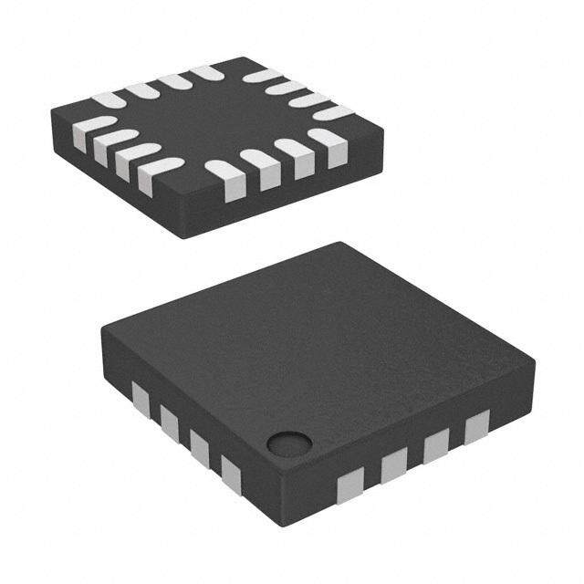
ICGOO电子元器件商城为您提供STMPE821QTR由STMicroelectronics设计生产,在icgoo商城现货销售,并且可以通过原厂、代理商等渠道进行代购。 STMPE821QTR价格参考¥询价-¥询价。STMicroelectronicsSTMPE821QTR封装/规格:接口 - 传感器,电容式触摸, Capacitive Touch Buttons 16-QFN (2.6x1.8)。您可以下载STMPE821QTR参考资料、Datasheet数据手册功能说明书,资料中有STMPE821QTR 详细功能的应用电路图电压和使用方法及教程。
| 参数 | 数值 |
| 产品目录 | |
| 描述 | IC CTLR TOUCH KEY 8CH CAP 16-QFN |
| 产品分类 | 电容式触摸传感器,接近传感器 IC |
| 品牌 | STMicroelectronics |
| 数据手册 | |
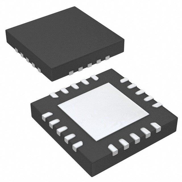
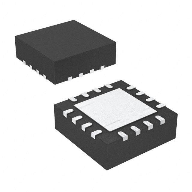
| 产品图片 |
|
| 产品型号 | STMPE821QTR |
| rohs | 无铅 / 符合限制有害物质指令(RoHS)规范要求 |
| 产品系列 | - |
| 产品培训模块 | http://www.digikey.cn/PTM/IndividualPTM.page?site=cn&lang=zhs&ptm=30444 |
| 产品目录页面 | |
| 供应商器件封装 | 16-QFN(2.6x1.8) |
| 其它名称 | 497-8826-1 |
| 分辨率(位) | - |
| 包装 | 剪切带 (CT) |
| 安装类型 | 表面贴装 |
| 封装/外壳 | 16-UFQFN |
| 工作温度 | -40°C ~ 85°C |
| 数据接口 | I²C |
| 数据速率/采样率(SPS,BPS) | - |
| 标准包装 | 1 |
| 特色产品 | http://www.digikey.com/cn/zh/ph/st/stmpe.html |
| 电压-电源 | 1.65 V ~ 1.95 V |
| 电压基准 | - |
| 电流-电源 | - |
| 类型 | 电容性 |
| 触摸面板接口 | - |
| 评估工具 | 可供 |
| 输入/按键数 | 8 键 |




- 商务部:美国ITC正式对集成电路等产品启动337调查
- 曝三星4nm工艺存在良率问题 高通将骁龙8 Gen1或转产台积电
- 太阳诱电将投资9.5亿元在常州建新厂生产MLCC 预计2023年完工
- 英特尔发布欧洲新工厂建设计划 深化IDM 2.0 战略
- 台积电先进制程称霸业界 有大客户加持明年业绩稳了
- 达到5530亿美元!SIA预计今年全球半导体销售额将创下新高
- 英特尔拟将自动驾驶子公司Mobileye上市 估值或超500亿美元
- 三星加码芯片和SET,合并消费电子和移动部门,撤换高东真等 CEO
- 三星电子宣布重大人事变动 还合并消费电子和移动部门
- 海关总署:前11个月进口集成电路产品价值2.52万亿元 增长14.8%



PDF Datasheet 数据手册内容提取
STMPE821 ® S-Touch 8-channel capacitive touchkey controller Features ■ Up to 8 GPIOs ■ Up to 8 capacitive touch key inputs ) s ■ Operating voltage 2.7-3.6 ( t ■ Internal regulator c u ■ Interrupt output pin d ■ I2C interface (1.8V operation, 3.3V tolerant) o r P ■ 8kV HBM ESD protection e ■ 50fF resolution, 128 steps capacitance t e measurement QFN16 l o ■ Advanced data filtering (AFS) (2.6x1.8mm) s b ■ Environment tracking calibration (ETC) O ■ Individually adjustable touch variance (TVR) - setting for all channels ) s ■ Adjustable environmental variance (EVR) for ( optimal calibration t c ■ Capacitive key sensing capabuility in 25μA Description d sleep mode o The STMPE821 is an 8-channel capacitive touch r Applications P key controller. The capacitance measurement is implemented fully in optimized hardware. e ■ Mobile and smartphones e t All 8 I/Os could be configured via I2C bus to ■ Portoalble media players function as either capacitive touchkey, or GPIO ■ Gsame consoles (general purpose I/O). b O Table 1. Device summary Order code Package Packing STMPE821QTR QFN16 (2.6 x 1.8 mm) Tape and reel November 2010 Doc ID 14478 Rev 5 1/50 www.st.com 50
Contents STMPE821 Contents 1 STMPE821 functional overview . . . . . . . . . . . . . . . . . . . . . . . . . . . . . . . . 5 1.1 STMPE821 block diagram . . . . . . . . . . . . . . . . . . . . . . . . . . . . . . . . . . . . . 5 1.2 Pin assignment and function . . . . . . . . . . . . . . . . . . . . . . . . . . . . . . . . . . . 6 1.3 STMPE821 typical application . . . . . . . . . . . . . . . . . . . . . . . . . . . . . . . . . . 7 1.4 Calibration algorithm . . . . . . . . . . . . . . . . . . . . . . . . . . . . . . . . . . . . . . . . . 8 1.4.1 Noise filtering . . . . . . . . . . . . . . . . . . . . . . . . . . . . . . . . . . . . . . . . . . . . . . 9 ) s 1.4.2 Data filtering . . . . . . . . . . . . . . . . . . . . . . . . . . . . . . . . . . . . . . . .( . . . . . . . 9 t c 1.5 Power management . . . . . . . . . . . . . . . . . . . . . . . . . . . . . . . u. . . . . . . . . . 10 d o 2 Power schemes . . . . . . . . . . . . . . . . . . . . . . . . . . . . . r. . . . . . . . . . . . . . . 11 P e 3 I2C interface . . . . . . . . . . . . . . . . . . . . . . . . . t. . . . . . . . . . . . . . . . . . . . . . 12 e l o s 4 Register map and function description . . . . . . . . . . . . . . . . . . . . . . . . . 14 b O 5 System and identification r-egisters . . . . . . . . . . . . . . . . . . . . . . . . . . . . 16 ) s ( 6 Interrupt controllert module . . . . . . . . . . . . . . . . . . . . . . . . . . . . . . . . . . 19 c u d 7 GPIO controoller . . . . . . . . . . . . . . . . . . . . . . . . . . . . . . . . . . . . . . . . . . . . 24 r P 8 Caepacitive touch module registers . . . . . . . . . . . . . . . . . . . . . . . . . . . . 26 t e l o 9 Basic PWM controller . . . . . . . . . . . . . . . . . . . . . . . . . . . . . . . . . . . . . . . 35 s b O 9.1 PWM function register map . . . . . . . . . . . . . . . . . . . . . . . . . . . . . . . . . . . 37 9.2 Interrupt on basic PWM controller . . . . . . . . . . . . . . . . . . . . . . . . . . . . . . 41 10 Maximum rating . . . . . . . . . . . . . . . . . . . . . . . . . . . . . . . . . . . . . . . . . . . . 42 11 Electrical specifications . . . . . . . . . . . . . . . . . . . . . . . . . . . . . . . . . . . . . 43 12 Package mechanical data . . . . . . . . . . . . . . . . . . . . . . . . . . . . . . . . . . . . 45 13 Revision history . . . . . . . . . . . . . . . . . . . . . . . . . . . . . . . . . . . . . . . . . . . 49 2/50 Doc ID 14478 Rev 5
STMPE821 List of tables List of tables Table 1. Device summary. . . . . . . . . . . . . . . . . . . . . . . . . . . . . . . . . . . . . . . . . . . . . . . . . . . . . . . . . . 1 Table 2. Pin assignments and function. . . . . . . . . . . . . . . . . . . . . . . . . . . . . . . . . . . . . . . . . . . . . . . . 6 Table 3. Calibration action under different scenarios. . . . . . . . . . . . . . . . . . . . . . . . . . . . . . . . . . . . . 8 Table 4. Operation modes . . . . . . . . . . . . . . . . . . . . . . . . . . . . . . . . . . . . . . . . . . . . . . . . . . . . . . . . 13 Table 5. Register summary map table . . . . . . . . . . . . . . . . . . . . . . . . . . . . . . . . . . . . . . . . . . . . . . . 14 Table 6. System and identification registers map. . . . . . . . . . . . . . . . . . . . . . . . . . . . . . . . . . . . . . . 16 Table 7. Sensor clock setting . . . . . . . . . . . . . . . . . . . . . . . . . . . . . . . . . . . . . . . . . . . . . . . . . . . . . . 18 Table 8. GPIO controller registers summary map. . . . . . . . . . . . . . . . . . . . . . . . . . . . . . . . . . . . . . . 24 Table 9. GPIO control bits function. . . . . . . . . . . . . . . . . . . . . . . . . . . . . . . . . . . . . . . . . . . . . . . . . . 25 ) Table 10. TOUCH_FIFO summary table . . . . . . . . . . . . . . . . . . . . . . . . . . . . . . . . . . . . . . . . . .s . . . . 26 ( Table 11. PWM function register map summary table . . . . . . . . . . . . . . . . . . . . . . . . . . . . t. . . . . . . . 37 c Table 12. Absolute maximum ratings. . . . . . . . . . . . . . . . . . . . . . . . . . . . . . . . . . . . . .u . . . . . . . . . . . 42 Table 13. DC electrical characteristics (-40 - 85 °C unless otherwise stated) . . . . d. . . . . . . . . . . . . . 43 o Table 14. Mechanical data for QFN16 (2.6x1.8 x 0.55mm) - 0.40mm pitch. . . . . . . . . . . . . . . . . . 46 r Table 15. Document revision history . . . . . . . . . . . . . . . . . . . . . . . . . . . . .P . . . . . . . . . . . . . . . . . . . . 49 e t e l o s b O - ) s ( t c u d o r P e t e l o s b O Doc ID 14478 Rev 5 3/50
List of figures STMPE821 List of figures Figure 1. Functional block diagram . . . . . . . . . . . . . . . . . . . . . . . . . . . . . . . . . . . . . . . . . . . . . . . . . . . 5 Figure 2. STMPE821 pin assignment (top view) . . . . . . . . . . . . . . . . . . . . . . . . . . . . . . . . . . . . . . . . . 6 Figure 3. Typical application diagram . . . . . . . . . . . . . . . . . . . . . . . . . . . . . . . . . . . . . . . . . . . . . . . . . 7 Figure 4. STMPE821 operating states. . . . . . . . . . . . . . . . . . . . . . . . . . . . . . . . . . . . . . . . . . . . . . . . 10 Figure 5. Power using the internal regulator . . . . . . . . . . . . . . . . . . . . . . . . . . . . . . . . . . . . . . . . . . . 11 Figure 6. Read and write modes (random and sequential) . . . . . . . . . . . . . . . . . . . . . . . . . . . . . . . . 13 Figure 7. Interrupt controller module block diagram . . . . . . . . . . . . . . . . . . . . . . . . . . . . . . . . . . . . . 19 Figure 8. Pulses with programmable brightness, ON/OFF period and repetition. . . . . . . . . . . . . . . . 35 Figure 9. Ramps with programmable brightness, ON/OFF period and repetition . . . . . . . . . . . . . . . 36 ) Figure 10. Fixed brightness output . . . . . . . . . . . . . . . . . . . . . . . . . . . . . . . . . . . . . . . . . . . . . . .s . . . . 36 ( Figure 11. Package outline for QFN16 (2.6x1.8 x 0.55mm) - 0.40mm pitch . . . . . . . . . . t. . . . . . . . 45 c Figure 12. Footprint recommendations for QFN16 (2.6x1.8 x 0.55mm) - 0.40mm pituch . . . . . . . . . 46 Figure 13. Carrier tape for QFN16 (2.6x1.8 x 0.55mm) - 0.40mm pitch . . . . . . . d. . . . . . . . . . . . . . 47 o Figure 14. Reel information for QFN16 (2.6x1.8 x 0.55mm) - 0.40mm pitch. . . . . . . . . . . . . . . . . . 48 r P e t e l o s b O - ) s ( t c u d o r P e t e l o s b O 4/50 Doc ID 14478 Rev 5
STMPE821 STMPE821 functional overview 1 STMPE821 functional overview The STMPE821 consists of the following blocks: ● GPIO controller ● PWM controller ● Impedance sensor ● Touch key controller ● I2C interface ) 1.1 STMPE821 block diagram s ( t c Figure 1. Functional block diagram u d o r P e t e l o s b GPIO 0 - 7 O /Touch 0 - 7 GPIO cont roller - ) s ( t c u PWM d controller Impedan ce o sensor r P INT e 2 e t RST intIe rCfac e Tcoonutcrhoklleeyr ARef l SCLK o SDAT s b O GND VCC VIO CS00046 Doc ID 14478 Rev 5 5/50
STMPE821 functional overview STMPE821 1.2 Pin assignment and function Figure 2. STMPE821 pin assignment (top view) 12 11 10 9 13 8 14 7 ) STMPE821 s ( 15 6 t c u d 16 5 o 1 2 3 4 r P e t e l o s CS00045 b O T able 2. Pin assignments and function - Pin number Pin name) Description s 1 GPIO_2/T(ouch_2 GPIO 2 t c 2 GPuIO_1/Touch_1 GPIO 1 d 3 o GPIO_0/Touch_0 GPIO 0 r 4P ARef Reference capacitor for touch sensor e RESET (active low). 5 RST t Pull to V for normal operation, pull to GND to reset. e CC ol 6 SDA I2C data s b 7 SCL I2C clock O 8 INT INT output (open drain) 9 GND GND 10 V Supply voltage for I2C block CC 11 V Supply voltage for GPIO and internal regulator IO 12 GPIO_7/Touch_7 GPIO 7 13 GPIO_6/Touch_6 GPIO 6 14 GPIO_5/Touch_5 GPIO 5 15 GPIO_4/Touch_4 GPIO 4 16 GPIO_3/Touch_3 GPIO 3 6/50 Doc ID 14478 Rev 5
STMPE821 STMPE821 functional overview 1.3 STMPE821 typical application The STMPE821 is able to support up to 8 channel capacitive sensors. Figure 3. Typical application diagram ) s (cid:51)(cid:52)(cid:45)(cid:48)(cid:37)(cid:24)(cid:18)(cid:17) ( t c (cid:50)(cid:51)(cid:52) u (cid:41)(cid:46)(cid:52) d (cid:34)(cid:65)(cid:83)(cid:69)(cid:66)(cid:65)(cid:78)(cid:68)(cid:15)(cid:35)(cid:48)(cid:53) o (cid:51)(cid:35)(cid:44)(cid:43) r (cid:51)(cid:36)(cid:33)(cid:52) P e (cid:33)(cid:50)(cid:69)(cid:70) t e l o s b O - ) s ( t c u (cid:33)(cid:45)(cid:16)(cid:16)(cid:23)(cid:16)(cid:22)(cid:54)(cid:17) d o r P e t e l o s b O Doc ID 14478 Rev 5 7/50
STMPE821 functional overview STMPE821 1.4 Calibration algorithm The STMPE821 maintains 2 parameters for each TOUCH channel: TVR and CALIBRATED IMPEDANCE. CALIBRATED IMPEDANCE is an internal reference of which, if the currently measured IMPEDANCE exceeds the CALIBRATED IMPEDANCE by a magnitude of TVR, it is considered a TOUCH. If the IMPEDANCE is more than the CALIBRATED IMPEDANCE, but the magnitude does not exceed CALIBRATED IMPEDANCE by TVR, it is not considered a TOUCH. In this case, 2 scenarios are possible: 1. Environmental changes has caused the IMPEDANCE to increase 2. Finger is near the sensing pad, but not near enough ) s In case 1, the change in IMPEDANCE is expected to be small, as environmental changes ( are normally gradual. A value "EVR" is maintained to specify the maximum IMcPtEDANCE change that is still considered an environmental change. u d o T able 3. Calibration action under different scenarios r P Scenario Touch se nsing and calibration action e TOUCHe, t IMP>CALIBRATED IMP + TVR no clalibration o s IMP<CALIBRATED IMP + TVR NO TOUCH, b IMP>CALIBRATED IMP + EVR O no calibration IMP<CALIBRATED IMP + TVR - NO TOUCH, IMP<CALIBRATED IMP + EVR ) new CALIBRATED IMP = previous CALIBRATED s IMP>CALIBRATED IMP ( IMP + change in IMP t c IMP>CALIBRATED IMuP CALIBRATED IMP + change in IMP d NO TOUCH, IMP<CALIBRAoTED IMP r new CALIBRATED IMP = new IMP P ‘IMP’ and ‘CALIBRATED IMP’ used in this table is not the direct register read-out. e t eIMP = 127 - impedance register read-out l o CALIBRATED IMP = 127 - calibrated impedance register read out. s b ETC WAIT register state a period of time of which, all TOUCH inputs must remain "NO O TOUCH" for the next calibration to be carried out. CAL INTERVAL states the period of time between successive calibrations when there are prolonged NO TOUCH condition. 8/50 Doc ID 14478 Rev 5
STMPE821 STMPE821 functional overview 1.4.1 Noise filtering When the STMPE821 is operating in the vicinity of highly emissive circuits (DC-DC converter, PWM controller/drive etc), the sensor inputs will be affected by high-frequency noise. In this situation, the time-integrating function could be used to distinguish between real touch, or emission-related false touch. The INTEGRATION TIME and STRENGTH THRES registers are used to configure the time- integrating function of STMPE821. 1.4.2 Data filtering The output from the calibration unit is an instantaneous "TOUCH" or "NO TOUCH" status. This output is directed to the filtering stage where the TOUCH is integrated across a ) s programmable period of time. The output of the integration stage would be a "ST(RENGTH" t (in STRENGTH register) that indicates the number of times a "TOUCH" is seecn, across the u integration period. d o The "STRENGTH" is then compared with the value in "STRENGTH THRESHOLD" register. r If STRENGTH exceeds the STRENGTH THRESHOLD, this is cPonsidered a final, filtered TOUCH status. e t In data filtering stage, 3 modes of operation is supporeted: l o Mode 1: Only the “touch” channel with highest STRENGTH is taken s b Mode 2: All the “touch” channels with STRENGTH > STRENGTH THRESHOLD is taken O Mode 3: The 2 “touch” channel with the highest STRENGTH is taken. These modes are - selected using the FEATURE SE LECTOR register. ) s The final, filtered data is a(ccessible through the Touch Byte register. t c u d o r P e t e l o s b O Doc ID 14478 Rev 5 9/50
STMPE821 functional overview STMPE821 1.5 Power management The STMPE821 operates in 3 states. Figure 4. STMPE821 operating states (cid:50)(cid:37)(cid:51)(cid:37)(cid:52) (cid:0) (cid:33)(cid:35)(cid:52)(cid:41)(cid:54)(cid:37) (cid:0) (cid:8)(cid:22)(cid:14)(cid:21)(cid:0)(cid:45)(cid:40)(cid:90)(cid:9) (cid:40)(cid:79)(cid:83)(cid:84)(cid:0)(cid:67)(cid:79)(cid:77)(cid:77)(cid:65)(cid:78)(cid:68) (cid:0) ) (cid:40)(cid:79)(cid:83)(cid:84)(cid:0)(cid:67)(cid:79)(cid:77)(cid:0)(cid:77)(cid:65)(cid:78)(cid:68) s ( t c (cid:52)(cid:79)(cid:85)(cid:67)(cid:72)(cid:12)(cid:0)(cid:72)(cid:79)(cid:84)(cid:75)(cid:69)(cid:89)(cid:12)(cid:0) (cid:40)(cid:79)(cid:84)(cid:75)(cid:69)(cid:89) (cid:0) u (cid:73)(cid:78)(cid:84)(cid:69)(cid:82)(cid:82)(cid:85)(cid:80)(cid:84)(cid:0)(cid:65)(cid:78)(cid:68)(cid:0)(cid:0) d (cid:72)(cid:79)(cid:83)(cid:84)(cid:0)(cid:67)(cid:79)(cid:77)(cid:77)(cid:65)(cid:78)(cid:68) o r (cid:40)(cid:79)(cid:83)(cid:84)(cid:0)(cid:67)(cid:79)(cid:77)(cid:77)(cid:65)(cid:78)(cid:68) (cid:0) P (cid:51)(cid:44)(cid:37)(cid:37)(cid:48) (cid:0) (cid:40)(cid:41)(cid:34)(cid:37)(cid:50)(cid:46)(cid:33)(cid:52)(cid:37)(cid:0) e (cid:8)(cid:18)(cid:16)(cid:16)(cid:0)(cid:43)(cid:40)(cid:90)(cid:9) t e l o s b O (cid:33)(cid:45)(cid:16)(cid:16)(cid:23)(cid:16)(cid:21)(cid:54)(cid:18) On RESET, the STMPE821 enters- the ACTIVE state immediately. ) Upon a fixed period of inactivsity, the device enters into the SLEEP state. Any touch activity in ( SLEEP state would causte the device to go back to ACTIVE state. c u In SLEEP mode: d o -Calibration continues if F2A bit is set in CONTROL register r P -Calibration stops if F2A bit is NOT set in CONTROL register e Itf no touch activity is expected, the host may set the device into HIBERNATE state to save e power. l o s If any key is touched and held, the I2C command to enter sleep or hibernate will be put on b hold, until the key has been released. O 10/50 Doc ID 14478 Rev 5
STMPE821 Power schemes 2 Power schemes The STMPE821 is powered by a 2.7 - 3.6V supply. An internal LDO regulates this supply into 1.8V for core operation. All GPIOs operates at V domain. IO Figure 5. Power using the internal regulator VIO 2.7-3.6V s ) ( t c u STMPE821 VCC d o * r P e GND t e l o s b O * recommended at least 1 μF - AM00736V1 ) s ( t c u d o r P e t e l o s b O Doc ID 14478 Rev 5 11/50
I2C interface STMPE821 2 3 I C interface The features that are supported by the I2C interface are the following ones: ● I2C slave device ● Compliant to Philips I2C specification version 2.1 ● Supports standard (up to 100kbps) and fast (up to 400kbps) modes. ● 7-bit and 10-bit device addressing modes ● General call ● Start/Restart/Stop ● I2C address is 0x58 (0xB0/0xB1 for write/read, including the LSB) ) s SCL/SDA level must be ≤ 3.6V t( c u Start condition d A Start condition is identified by a falling edge of SDATA while SCLK ois stable at high state. r A Start condition must precede any data/command transfer. TheP device continuously monitors for a Start condition and will not respond to any tra nsaction unless one is e encountered. t e Stop condition l o s A Stop condition is identified by a rising edge of SDATA while SCLK is stable at high state. b A Stop condition terminates communicaOtion between the slave device and bus master. A read command that is followed by N oAck can be followed by a Stop condition to force the - slave device into idle mode. Whe n the slave device is in idle mode, it is ready to receive the ) next I2C transaction. A Stop csondition at the end of a write command stops the write ( operation to registers. t c Acknowledge bit (AuCK) d The acknowleodge bit is used to indicate a successful byte transfer. The bus transmitter r releasesP the SDATA after sending eight bits of data. During the ninth bit, the receiver pulls the S DATA low to acknowledge the receipt of the eight bits of data. The receiver may leave e the SDATA in high state if it would to not acknowledge the receipt of the data. t e l Data Input o s The device samples the data input on SDATA on the rising edge of the SCLK. The SDATA b O signal must be stable during the rising edge of SCLK and the SDATA signal must change only when SCLK is driven low. Memory addressing For the bus master to communicate to the slave device, the bus master must initiate a Start condition and followed by the slave device address. Accompanying the slave device address, there is a Read/WRITE bit (R/W). The bit is set to 1 for read and 0 for write operation. If a match occurs on the slave device address, the corresponding device gives an acknowledgement on the SDA during the 9th bit time. If there is no match, it deselects itself from the bus by not responding to the transaction. 12/50 Doc ID 14478 Rev 5
STMPE821 I2C interface Table 4. Operation modes Mode Byte Programming sequence Start, Device address, R/W=0, Register address to be read Restart, Device address, R/W=1, Data Read, STOP If no Stop is issued, the Data Read can be continuously performed. If the register address falls within the range that allows an address auto- Read ≥1 increment, then the register address auto-increments internally after every byte of data being read. For those register addresses that fall within a non-incremental address range, the address will be kept static throughout the entire write operations. Refer to the memory map table for the address ranges that are auto and non-increment. An example of such a non-increment address is FIFO s ) ( Start, Device address, R/W=0, Register address to be wtritten, Data c Write, Stop u d If no Stop is issued, the Data Write can be continuously performed. If o the register address falls within the range that allows address auto- r increment, then the register address autPo-increments internally after Write ≥1 every byte of data being written in. F or those register addresses that e fall within a non-incremental adtdress range, the address will be kept e static throughout the entire write operations. Refer to the memory map l table for the address ranoges that are auto and non-increment. An s example of a non-increment address is Data port for initializing the b PWM commands. O - Figure 6. Read and write mo des (random and sequential) ) s ( t OneR beyatde Startd ADduedvriecsecs R/W=0 Ack AdRderegss Ack Restart ADdedvriecses R/W=1 Ack RDeaatad No Ack Stop o r P tMoree th an oneR beyatde Start ADdedvriecses R/W=0 Ack AdRderegss Ack Restart ADdedvriecses R/W=1 Ack RDeaatad Ack ReDaadt a+ 1 Ack ReDaadt a+ 2 No Ack Stop e l o s O b OneW bryittee Start ADdedvriecses R/W=0 Ack AdRderegss Ack wtDoria tbtteaen Ack Stop More than one byte Read Start ADdedvriecses R/W=0 Ack AdRderegss Ack DWatrait eto Ack WDraittea +to 1 Ack WDraittea +to 2 Ack Stop Master Slave Doc ID 14478 Rev 5 13/50
Register map and function description STMPE821 4 Register map and function description This section lists and describes the registers of the STMPE821 device, starting with a register map and then provides detailed descriptions of register types. T able 5. Register summary map table Address Register name Bit Type Reset value Function 0x00 CHIP_ID_0 8 R 0x08 Device identification 0x01 CHIP_ID_1 8 R 0x21 Device identification 0x02 ID_VER 8 R 0x0F Revision number s ) ( 0x03 SYS_CFG_1 8 R/W 0x00 System configuratiton 1 c u 0x04 SYS_CFG_2 8 R/W 0xEF System configuration 2 d 0x08 INT_CTRL 8 R/W 0x01 Interrupot control register r 0x09 INT_EN 8 R/W 0x01 InPterrupt enable register e 0x0A INT_STA 8 R 0x01 Interrupt status register t e 0x0B GPIO__INT_EN_lsb 8 R/W 0x00 GPIO interrupt enable register l o 0x0C GPIO__INT_EN_msb 8 R/Ws 0x00 GPIO interrupt enable register b 0x0D GPIO_INT_STA_lsb 8 O R/W 0x00 GPIO interrupt status register 0x0E GPIO_INT_STA_msb -8 R/W 0x00 GPIO interrupt status register ) 0x10 GPIO_MR s 8 R/W 0x00 GPIO monitor pin ( 0x12 GPIO_SET t 8 R/W 0x00 GPIO set pin state register c u 0x14 GPIO_DIR 8 R/W 0x00 GPIO set pin direction register d 0x16 GPIoO_FUNCT 8 R/W 0x00 GPIO function register r P 0x18 TOUCH_FIFO 64 R 0x00 Fifo access for touch data buffer e 0x20 FEATURE_SEL 8 R/W 0x04 Feature selection t e l 0x21 ETC_WAIT 8 R/W 0x27 Wait time o s 0x22 CAL_INTERVAL 8 R/W 0x30 Calibration interval b O INTEGRATION_ 0x23 8 R/W 0x0F Integration time TIME 0x25 CTRL 8 R/W 0x00 Control 0x26 INT_MASK 8 R/W 0x08 Interrupt mask 0x27 INT_CLR 8 R/W 0x00 Interrupt clear 0x28 FILTER_PERIOD 8 R/W 0x00 Filter period FILTER_THRESHOL 0x29 8 R/W 0x00 Filter threshold D 0x2A REF_DLY 8 R/W 0x00 Reference delay 0x30 - TVR 8 R/W 0x08 Touch variance setting 0x37 14/50 Doc ID 14478 Rev 5
STMPE821 Register map and function description Table 5. Register summary map table (continued) Address Register name Bit Type Reset value Function 0x40 EVR 8 R/W 0x04 Environmental variance 0x50 - STRENGTH_THRES Setting of strength threshold for 8 R/W 0x01 0x57 [0-7] each channel 0x60 - STRENGTH [0-7] 8 R 0x00 Strength 0x67 0x70 - CAL_IMPEDANCE 8 R 0x00 Calibrated impedance 0x77 [0-7] 0x80 - IMPEDANCE [0-7] 8 R 0x00 Impedance ) 0x87 s ( Status of GINT intetrrupt 0x92 INT_PENDING 8 R/W 0x00 c sources u d 0xA0 PWM_OFF_OUTPUT 8 R/W 0x00 PWM goroup control r 0xA1 MASTER_EN 8 R/W 0x00 MPaster enable 0xB0 PWM0_SET 8 R/W 0x00 e PWM 0 setup t 0xB1 PWM0_CTRL 8 R/W 0ex00 PWM 0 control l o 0xB2 PWM0_RAMP_RATE 8 R/W 0x00 PWM 0 ramp rate s b 0xB4 PWM1_SET 8 R/W 0x00 PWM 1 setup O 0xB5 PWM1_CTRL 8 R/W 0x00 PWM 1 control - 0xB6 PWM1_RAMP_RATE ) 8 R/W 0x00 PWM 1 ramp rate s ( 0xB8 PWM2_SET t 8 R/W 0x00 PWM 2 setup c 0xB9 PWM2_CTuRL 8 R/W 0x00 PWM 2 control d 0xBA PWoM2_RAMP_RATE 8 R/W 0x00 PWM 2 ramp rate r 0xBC P PWM3_SET 8 R/W 0x00 PWM 3 setup 0exBD PWM3_CTRL 8 R/W 0x00 PWM 3 control t e 0xBE PWM3_RAMP_RATE 8 R/W 0x00 PWM 3 ramp rate l o s b O Doc ID 14478 Rev 5 15/50
System and identification registers STMPE821 5 System and identification registers Table 6. System and identification registers map Address Register name Bit Type Reset Function Device 0x00 CHIP_ID_0 8 R 0x08 identification Device 0x01 CHIP_ID_1 8 R 0x21 identification 0x02 ID_VER 8 R 0x0F Revision number ) System s 0x03 SYS_CFG_1 8 R/W 0x00 configu(ration 1 t c uSystem 0x04 SYS_CFG_2 8 R/W 0xEF d configuration 2 o r P e CHIP_ID_x Device identification t e Address: 0x00, 0x01 ol s Type: R b O Description: 8-bit device identification - ) s ( t c u d o r P e t e l o s b O 16/50 Doc ID 14478 Rev 5
STMPE821 System and identification registers ID_VER Revision number Address: 0x02 Type: R Reset: 0x0F Description: 16-bit revision number SYS_CFG_1 System configuration 1 7 6 5 4 3 2 1 0 RESERVED SLEEP WARM_RESET SOFT_RESET HIBERNATE ) s Address: 0x03 ( t c Type: R/W u d Reset: 0x00 o r Description: The reset control register enables to reset the device P [7:4] RESERVED e t [3] SLEEP: e l Write ‘1’ to enable sleep mode. hardware resetso this bit to ‘0’ after it successfully enters sleep mode. s b [2] WARM_RESET: O Write ‘1’ to initiate a warm reset. Register content remains, state machine reset. - [1] SOFT_RESET: ) s Write ‘1’ to initiate a so(ft reset. All registers content and state machines reset. t c [0] HIBERNATE: Fuorce the device into hibernation mode. Write ‘1’ to denter the hibernate mode. Hardware resets this bit to ‘0’ after it successfully enters o hibernate mode. r P e t e l o s b O Doc ID 14478 Rev 5 17/50
System and identification registers STMPE821 SYS_CFG_2 System configuration 2 7 6 5 4 3 2 1 0 SENSOR SENSOR SENSOR PWM CLOCK GPIO CLOCK FIFO CLOCK TOUCH CLOCK - CLOCK 2 CLOCK 1 CLOCK 0 DISABLE DISABLE DISABLE DISABLE Address: 0x04 Type: R/W Reset: 0xEF Description: This register enables to switch off the clock supply [7:5] SENSOR CLOCK: See description in the table below. ) [4] RESERVED s ( t [3] PWM CLOCK DISABLE: c u Write ‘1’ to disable the clock to PWM unit. d [2] GPIO CLOCK DISABLE: o r Write ‘1’ to disable the clock to GPIO unit. Note that GPIO clockP is required for PWM operation. [1] FIFO CLOCK DISABLE: e t Write ‘1’ to disable the clock to FIFO unit. This must ebe set to ‘0’ if touch interrupt is required. l [0] TOUCH CLOCK DISABLE: o s Write ‘1’ to disable the clock to TOUCH unit. b O T able 7. Sensor clock setting- ) s Sensor clock Mode Di(vider Active Calibration t [2:0] c u 1 000 12.8KHz 100KHz d o 2 001 6.4KHz 50KHz r OperationP al 4 010 3.2KHz 25KHz (6.5M Hz) e 8 011 1.6KHz 12.5KHz t e l 16 1xx 800Hz 6.25KHz o s 1 000 400Hz 3.2KHz b O 2 001 200Hz 1.6KHz Autosleep 4 010 100Hz 800Hz (200KHz) 8 011 50Hz 400Hz 16 1xx 25Hz 200Hz 18/50 Doc ID 14478 Rev 5
STMPE821 Interrupt controller module 6 Interrupt controller module Figure 7. Interrupt controller module block diagram Interrupt INT status pending INT AND ) s Interrupt ( INT enable ct mask u d o r P e GPIO t e interrupt l status o s AND b O GPIO - interrupt ) enable s ( t c u d o CS00053 r P e t e l o s b O Doc ID 14478 Rev 5 19/50
Interrupt controller module STMPE821 INT_CTRL Interrupt control register 7 6 5 4 3 2 1 0 POLARITY TYPE INT_EN Address: 0x08 Type: R/W Reset: 0x00 Description: This register is used to enable control the polarity, edge/level and enabling of the interrupt system.device [7:3] RESERVED ) s [2] POLARITY: ( t '0' for active low c u '1' for active high d For active low operation, the INT pin should be externally pulled higho (up to 3.3V, but ≤ VIO). The INT pin will be pulled to GND when there is a pending interrurpt. P For active high operation, the INT pin should be externally pulled to GND. In this mode, the INT pin will be pulled to V by the device when there is a peneding interrupt. CC t e [1] TYPE: l o '0' for level trigger s '1' for edge trigger (pulse width is 200nSb) O [0] INT_EN: '0' to disable all interrupt - ) '1' to enable all interrupt s ( t c u d o r P e t e l o s b O 20/50 Doc ID 14478 Rev 5
STMPE821 Interrupt controller module INT_EN Interrupt enable register 7 6 5 4 3 2 1 0 GPIO PWM3 PWM2 PWM1 PWM0 GEN FIFO POR Address: 0x09 Type: R/W Reset: 0x00 Description: This register is used to enable the interruption from a system related interrupt source to the host. Writing ‘1’ in this register enables the corresponding interrupt event to generate interrupt signal at the INT pin. Note that even if the interrupt is not enabled, an interrupt event will still be reflected in the interrupt status register. s ) ( . t c u [7] GPIO: d One or more level transition in enabled GPIOs o r [6] PWM3: P Completion of PWM sequence e t [5] PWM2: e l Completion of PWM sequence o s [4] PWM1: b Completion of PWM sequence O [3] PWM0: - ) Completion of PWM sequsence ( [2] GEN: t c System INT (A2u1, I2A, EOC) d [1] FIFO: o Datar available in FIFO. This interrupt can be cleared only if FIFO is empty. P [0] POR: e t Power-on reset e l o INTs_STA Interrupt status register b O 7 6 5 4 3 2 1 0 GPIO PWM3 PWM2 PWM1 PWM0 GEN FIFO POR Address: 0x0A Type: R Reset: 0x00 Description: This register is used to enable the interruption from a system related interrupt source to the host. Regardless whether the IESYSIOR bits are enabled, the ISSYSIOR bits Doc ID 14478 Rev 5 21/50
Interrupt controller module STMPE821 are still updated. Writing ‘1’ clears a bit in this register. Writing ‘0’ has no effect. [7] GPIO: One or more level transition in enabled GPIOs [6] PWM3: Completion of PWM sequence [5] PWM2: Completion of PWM sequence [4] PWM1: Completion of PWM sequence [3] PWM0: ) Completion of PWM sequence s ( [2] GEN: t c System INT (A21, I2A, EOC) u d [1] FIFO: o Data available in FIFO r P [0] POR: e Power-on reset t e l o s GPIO_INT_EN b GPIO interrupt enable registerI O 7 6 5 4 3 2 1 0 - IEG[x] ) s Address: 0x0B, 0x0C ( t c Type: R/W u d Reset: 0x00 o r Description: ThPe GPIO interrupt enable register is used to enable the interruption from a particular e GPIO interrupt source to the host. The IEg[7:0] bits and the interrupt enable mask bits t correspond to the GPIO[7:0} pins. e ol [7:0] IEG[7:0] s Interrupt enable GPIO mask (where x=7 to 0) b O Writing a ‘1’ to the IE[x] bit will enable the interruption to the host. 22/50 Doc ID 14478 Rev 5
STMPE821 Interrupt controller module GPIO_INT_STA GPIO interrupt status register 7 6 5 4 3 2 1 0 Address: 0x0D Type: R/W Reset: 0x00 Description: The GPIO interrupt status register LSB monitors the status of the interruption from a particular GPIO pin interrupt source to the host. Regardless whether the IEGPI)OR s bits are enabled or not, the INT_STA_GPIO_LSB bits are still updated. The ISG[7:0] ( bits are the interrupt status bits correspond to the GPIO[7:0] pins. ct u [7:0] ISG[x]: d Interrupt status GPIO (where x = 7 to 0) o Read: P r Interrupt status of the GPIO[x]. Writing ‘1’ clears a bit. Writin g ‘0’ has no effect. e t e l o s b O - ) s ( t c u d o r P e t e l o s b O Doc ID 14478 Rev 5 23/50
GPIO controller STMPE821 7 GPIO controller A total of 8 GPIOs are available in the STMPE821. The GPIO controller contains the registers that allow the host system to configure each of the pins into either a GPIO, direct output of a TOUCH channel or a PWM output. Unused GPIOs should be configured as outputs to minimize the power consumption. A group of registers is used to control the exact function of each of the 8 GPIOs. The registers and their respective address is listed in the following table. T able 8. GPIO controller registers summary map ) Address Register name Description Auto-incremsent ( 0x10 GPIO_MR_LSB GPIO monitor pin state ct u YES 0x11 GPIO_MR_MSB register d o 0x12 GPIO_SET_LSB GPIO set pin state r register P YES 0x13 GPIO_SET_MSB e 0x14 GPIO_DIR_LSB GPIO sett pin direction e YES register 0x15 GPIO_DIR_MSB l o s 0x16 GPIO_FUNCT_LSB b GPIO function register YES 0x17 GPIO_FUNCT_MO SB - All GPIO registers are named as GPxx, where: ) s Xxx represents the functio(nal group t c For LSB registers: u d o r 7 6 P 5 4 3 2 1 0 IO-7 IO-6 IO-5 IO-4 IO-3 IO-2 IO-1 IO-0 e t eFor MSB registers: l o s b O 7 6 5 4 3 2 1 0 RESERVED 24/50 Doc ID 14478 Rev 5
STMPE821 GPIO controller The function of each bit is shown in the following table: Table 9. GPIO control bits function Register name Function Reading this bit yields the current state of the bit. Writing has no GPIO monitor pin state effect. Writing '1' to this bit causes the corresponding GPIO to go to '1' state GPIO set pin state Writing '0' to this bit causes the corresponding GPIO to go to '0' state '0' sets the corresponding GPIO to input state, and '1' sets it to output GPIO set pin direction state. All bits are '0' on reset. The GPIO must be set as output if the PWM on this pin is to be used. ) s '1' sets the corresponding GPIO to function as GPIO/PWM(, and '0' t sets it to touch key mode. c u GPIO function For GPIO 0-3, if the GPIO function is set to GPIO/PWM mode and the d AF bits in the PWM master enable register iso enabled, the corresponding GPIO will function as PWMr output. P e t e l o s b O - ) s ( t c u d o r P e t e l o s b O Doc ID 14478 Rev 5 25/50
Capacitive touch module registers STMPE821 8 Capacitive touch module registers Table 10. TOUCH_FIFO summary table Address Function 0x18 FIFO-0, LSB 0x19 FIFO-0, MSB 0x1A FIFO-1, LSB 0x1B FIFO-1, MSB ) s 0x1C FIFO-2, LSB ( t c 0x1D FIFO-2, MSBu d 0x1E FIFO-o3, LSB r 0x1F FPIFO-3, MSB e TOUCH_FIFO t Touch FIFO e l 7 6 5 4 3 o 2 1 0 s T7 T6 T5 T4 T3 T2 T1 T0 b O Address: 0x19, 0x18 - ) Type: R s ( Reset: 0x00 t c u Description: TOUCH_FIFO is the access port for the internal 4-level FIFO used for buffering the d touch eovents. While it is possible to access each bytes in the data structure directly, it is rercommended that the FIFO is accessed only via the 0x18 address. P e The FIFO must be accessed in multiples of 2 bytes (LSB, MSB). For STMPE821, t MSB is reserved and LSB contains a snapshot of the recent touch event. The FIFO e l must be accessed in multiples of 2 bytes (LSB, MSB). For STMPE821, MSB is o reserved and LSB contains a snapshot of the recent touch event. s b Where Tn is touch status of touch sensing channel n. O 26/50 Doc ID 14478 Rev 5
STMPE821 Capacitive touch module registers FEATURE_SELECT Feature select 7 6 5 4 3 2 1 0 RESERVED AFS[1:0] Filter EN Address: 0x20 Type: R/W Reset: 0x04 Description: Controls AFS (advanced filtering system and second level filtering feature [7:3] RESERVED [2:1] AFS[1:0]: ) s “00’: reserved ( t “01’ AFS mode 1 (only 1 strongest key) c u ‘10’: AFS mode 2 (all keys that are above threshold) d ‘11’: AFS mode 3 (the 2 strongest keys) o r [0] Filter EN: P Write '1' to enable filter e t e l ETC_WAIT o Wait time setting s b 7 6 5 4 3 O 2 1 0 ET C_WAIT[7:0] - ) Address: 0x21 s ( Type: R/W t c u Reset: 0x27 d o Description: Sets the wait time between the calibration and the last button touch r P [7:0] ETC_WAIT[7:0]: e ETC wait time = ETC_Wait[7:0] *64 + sensor clock period t e l o A "non-touch" condition must persist for this wait time, before an ETC operation is carried out. s b O Range: 5mS - 20s Doc ID 14478 Rev 5 27/50
Capacitive touch module registers STMPE821 CAL_INTERVAL Calibration interval 7 6 5 4 3 2 1 0 CAL_INTERVAL Address: 0x22 Type: R/W Reset: 0x30 Description: Calibration interval [7:0] CALIBRATION INTERVAL: Interval between calibration = Calibration Interval [7:0] * sensor clock period * 50 ) s ( Range: 4mS - 16S ct u d o r INTEGRATION TIME P Integration time e 7 6 5 4 3 2 1 0 t e INTEGRATION_TIME[7:0] l o s Address: 0x23 b O Type: R/W - Reset: 0x0F ) s Description: Integration time ( t [7:0] Integration time inc AFS mode u d Total peoriod of integration = sensor clock period * Integration Time [7:0] r P 78μS - 320mS e t e l o s b O 28/50 Doc ID 14478 Rev 5
STMPE821 Capacitive touch module registers CTRL Control 7 6 5 4 3 2 1 0 RESERVED F2A HDC_U HDC_C HOLD Address: 0x25 Type: R/W Reset: 0x00 Description: Control [7:4] RESERVED [3] F2A: ) s Write '1' to force device to remain in ACTIVE state at all times ( t c [2] HDC_U: u Write '1' to perform unconditional host driven calibration. d o Cleared to '0' when calibration is completed r P Only applicable HOLD is '1' e t e l [1] HDC_C: o s Write '1' to perform conditional host driven calibration. b Calibration is performed if and only ifO no touch is detected. Cleared to '0' when calibration is completed - ) Only applicable HOLD is s'1' ( t c u [0] HOLD: d '0' to enaoble ETC '1' tor disable ETC P e t e l o s b O Doc ID 14478 Rev 5 29/50
Capacitive touch module registers STMPE821 INT_MASK Interrupt mask 7 6 5 4 3 2 1 0 RESERVED EOC RESERVED Address: 0x26 Type: R/W Reset: 0x08 Description: Writing '1' to this register disables the corresponding interrupt source. [7:4] RESERVED [3] EOC: ) s End of calibration ( t This interrupt occurs on both automatic and forced calibration c u [2:0] RESERVED d o r P INT_CLR Interrupt clear e t 7 6 5 4 3 2 e 1 0 l RESERVED EOC o RESERVED s Address: 0x27 b O Type: R/W - Reset: 0x00 ) s ( Description: Writing '1' to this rtegister clears the corresponding interrupt source in INT_PENDING c register. u d [7:4] RESERVED o [3] EOCr: P End of calibration e This interrupt occurs on both automatic and forced calibration t e l [2:0] RESERVED o s b O 30/50 Doc ID 14478 Rev 5
STMPE821 Capacitive touch module registers FILTER_PERIOD Filter period 7 6 5 4 3 2 1 0 FILTER_COUNT Address: 0x28 Type: R/W Reset: 0x00 Description: Filter period. [7:0] FILTER_COUNT: Additional filter to stabilize touch output in AFS mode. ) s ( AFS touch output is monitored for Filter Count [7:0] times every integration timec. Ftor each time a "touch status" is detected, an internal "Filter Counter" is incremented onceu. This counter value is then compared with Filter Threshold (register 0x3E) d o r P e FILTER_THRESHOLD Filter threshold t e l 7 6 5 4 3 o 2 1 0 s FILTER_THRESHOLD b O Address: 0x29 - Type: R/W ) s Reset: 0x00 ( t c Description: Filter thresholud. d [7:0] FILTER_THRESHOLD: o An inrternal "Filter Counter" is compared with Filter Threshold [7:0] to determine if a valid touch P has occurred. e t e REFERlENCE_DELAY Reference delay o s b 7 6 5 4 3 2 1 0 O RESERVED REFERENCE_DELAY Address: 0x2A Type: R/W Reset: 0x00 Description: Shifting of capacitive sensor dynamic range. The capacitance value set into this register is in effect, equivalent to capacitor connected to the A_Ref pin. [7] RESERVED [6:0] REFERENCE_DELAY: Valid range = 0-127 Each step represents capacitance value of 0.05pF Warm reset is required after this value is updated Doc ID 14478 Rev 5 31/50
Capacitive touch module registers STMPE821 TVR Touch variance setting 7 6 5 4 3 2 1 0 RESERVED TVR Address: 0X30 - 0x3B Type: R/W Reset: 0x08 Description: Touch variance setting. [7] RESERVED [6:0] TVR: ) s Setting TVR between 0-99 ( t A high TVR value decreases sensitivity of the sensor, but increasing its tolerancce to ambient u noise d A small TVR value increases the sensitivity. o r P EVR e Environmental variance t e 7 6 5 4 3 l2 1 0 o RESERVED TVRs b Address: 0x40 O Type: R/W - ) Reset: 0x04 s ( t Description: Environmental vcariance setting. u [7] RESERVEDd o [6] EVR: r P EVR is used to detect "Non-Touch" condition e t e STRENGTH_THRESHOLD Strength threshold l o s b 7 6 5 4 3 2 1 0 O STRENGTH_THRESHOLD Address: 0x50 - 0x57 Type: R/W Reset: 0x01 Description: Strength threshold. [7:0] STRENGTH_THRESHOLD: Setting threshold to be used in AFS mode to determine valid touch 32/50 Doc ID 14478 Rev 5
STMPE821 Capacitive touch module registers STRENGTH Strength 7 6 5 4 3 2 1 0 STRENGTH Address: 0x60 - 0x67 Type: R Reset: 0x00 Description: The number of times where a sense capacitance exceeds the calibrated reference impedance ) s [7:0] STRENGTH: ( t Read-only field c u Counts the number of times a sensed impedance exceeds calibrated reference impedance d over and integration time. Maximum strength equals Integration Timeo [7:0] r P e t e l o s b O - ) s ( t c u d o r P e t e l o s b O Doc ID 14478 Rev 5 33/50
Capacitive touch module registers STMPE821 CALIBRATED_IMPEDANCE Calibrated impedance 7 6 5 4 3 2 1 0 CAL_IMPEDANCE Address: 0x70 - 0x77 Type: R Reset: 0x00 Description: Calibrated impedance is a reference value maintained by the device. [7:0] CALIBRATED IMPEDANCE: Calibrated reference impedance ) s ( t IMPEDANCE cImpedance u d 7 6 5 4 3 2 o 1 0 r IMPEDANCE P Address: 0x80 - 0x87 e t e Type: R l o Reset: 0x00 s b Description: Impedance is the instantaneous iOmpedance value seen at the input pin of each cap. sensing pin. - [7:0] IMPEDANCE: ) s Currently sensed impedance. This impedance reading decreases with the increase of the ( capacitance at sensting channel. c When this regisuter reads 0x7F, reference capacitance should be reduced. d When this register reads 0x00, reference capacitance should be increased. o r P TINT_PENDIN G Interrupt pending e t e 7 6 5 4 3 2 1 0 l o s RESERVED EOC RESERVED b Address: 0x92 O Type: R/W Reset: 0x00 Description: Reflects the status of each interrupt source. [7:4] RESERVED [3] EOC: End of calibration [2:0] RESERVED 34/50 Doc ID 14478 Rev 5
STMPE821 Basic PWM controller 9 Basic PWM controller The advanced PWM allows complex brightness and blinking control of a LED. The basic PWM controller allows simpler brightness control and basic blinking patterns. The STMPE821 is fitted with a 4-channel basic PWM controller. The PWM controllers outputs are connected to the GPIO 0-3. In order to activate the PWM channels, the alternate function bits in the master enable register must be set to '1'. The PWM controllers are capable of generating the following brightness patterns: Figure 8. Pulses with programmable brightness, ON/OFF period and repetition ) s 1 time ( Duty unit t c cycle u d o r P e Time t e On Off ON Off l period period period o period s b O CS00054 - On period = period 0[1:0] * time) unit [3:0] s ( Off period = period 1[1:0t] * time unit [3:0] c u Duty cycle during “on period” = brightness [7:4] d Number of cycoles = repetition [3:0] r P Ramp mode is disabled e t e l o s b O Doc ID 14478 Rev 5 35/50
Basic PWM controller STMPE821 Figure 9. Ramps with programmable brightness, ON/OFF period and repetition 1 time Duty unit cycle Time ON Off ON Off ) s period period period period ( t c u d o P r CS00055 “On” period = period 0[1:0] * time unit [3:0] e t “Off” period = period 1[1:0] * time unit [3:0] e l o Duty cycle during “on” period = brightness [7:4] s b Number of cycles = repetition [3:0] O Ramp up rate is programmable. - ) s Figure 10. Fixed brightness output ( t c u d time unit Duty cycleo r P e t e l o s b Time O CS00056 “On” period = period 0[1:0] * time unit [3:0] Off period = don't care Duty cycle during “on” period = brightness [7:4] Number of cycles = repetition [3:0] = 0 (means infinite repetition) 36/50 Doc ID 14478 Rev 5
STMPE821 Basic PWM controller 9.1 PWM function register map T able 11. PWM function register map summary table Auto-increment Register name Description (during sequential R/W) Set the output level when PWM PWM_OFF_OUTPUT Yes is disabled Enables/disables individual MASTER_EN Yes basic PWM channels PWM0_SET PWM 0 setup Yes ) PWM0_CTRL PWM 0 control Yes s ( t PWM0_RAMP_RATE PWM 0 ramp rate Yesc u PWM1_SET PWM 1 setup d Yes o PWM1_CTRL PWM 1 control Yes r P RAMP1_RATE PWM 1 ramp rate Yes e PWM2_SET PWM 2 setup t Yes e PWM2_CTRL PWM 2 control ol Yes s RAMP2_RATE PWM 2 ramp rate Yes b O PWM3_SET PWM 3 setup Yes PWM3_CTRL P W-M 3 control Yes ) s PWM3_RATE PWM 3 ramp rate Yes ( t c MASTER_EN u Master enabler d 7 6 o 5 4 3 2 1 0 r AF3 AF2P AF2 AF0 EN3 EN2 EN1 EN0 e Address: 0xA1 t e Type: l R/W o s Reset: 0x00 b O Description: Write ‘1’ to select PWM function on the corresponding channel. [7:4] AF3:0 [3:0] OUT3:0: Default is '0'. Write ‘1’ to used the corresponding PWM channel must be diabled for the controlling registers to be accessed. Doc ID 14478 Rev 5 37/50
Basic PWM controller STMPE821 PWM_OFF_OUTPUT PWM group control register 7 6 5 4 3 2 1 0 OUT3 OUT2 OUT1 OUT0 Address: 0xA0 Type: R/W Reset: 0x00 Description: PWM group control register. [7:4] RESERVED ) s [3:0] OUT3:0: ( t Default is '0' c u '1' - PWM channel outputs '1' when disabled d '0' - PWM channel outputs '0' when disabled o r P RAMP_RATE e Ramp rate register t e 7 6 5 4 3 l 2 1 0 o RESERVED RAMP_DOWN s RAMP_UP b Address: 0xB2 O Type: R/W - ) Reset: 0x00 s ( t Description: Ramp rate regiscter. u [7:6] RESERVEDd o [5:3] RAMrP_DOWN [2:0]: P '000' = 1/4 of time unit per brightness level change e '001' = 1/8 of time unit per brightness level change t e '010' = 1/16 of time unit per brightness level change l o '011' = 1/32 of time unit per brightness level change s '100' = 1/64 of time unit per brightness level change b O '101' = 1/128 of time unit per brightness level change '110' = reserved '111' = reserved [2:0] RAMP_UP [2:0]: '000' = 1/4 of time unit per brightness level change '001' = 1/8 of time unit per brightness level change '010' = 1/16 of time unit per brightness level change '011' = 1/32 of time unit per brightness level change '100' = 1/64 of time unit per brightness level change '101' = 1/128 of time unit per brightness level change '110' = reserved '111' = reserved 38/50 Doc ID 14478 Rev 5
STMPE821 Basic PWM controller PWM_n_SETUP PWM_n setup register (n=0-3) 7 6 5 4 3 2 1 0 BRIGHTNESS TIMING Address: 0xB0 Type: R/W Reset: 0x00 Description: PWM setup register. [7:4] BRIGHTNESS: This defines the duty cycle during the ON period of the PWM channel output which in turn ) determines the brightness level of the LED that the PWM output drives. s ( 0000: Duty cycle ratio 1:15 (6.25%, minimum brightness) t c 0001: Duty cycle ratio 2:14 (12.50%) u 0010: Duty cycle ratio 3:13 (18.75%) d o 0011: Duty cycle ratio 4:12 (25.00%) r P 0100: Duty cycle ratio 5:11 (31.25%) 0101: Duty cycle ratio 6:10 (37.50%) e t 0110: Duty cycle ratio 7: 9 (43.75%) e 0111: Duty cycle ratio 8: 8 (50.00%) ol 1000: Duty cycle ratio 9: 7 (56.25%) s b 1001: Duty cycle ratio 10: 6 (62.50%)O 1010: Duty cycle ratio 11: 5 (68.75%) - 1011: Duty cycle ratio 12: 4 ( 75.00%) ) 1100: Duty cycle ratio 13s: 3 (81.25%) ( 1101: Duty cycle rattio 14: 2 (87.50%) c 1110: Duty cycule ratio 15: 1 (93.75%) d 1111: Duty cycle ratio 16: 0 (100.00%, maximum brightness) o [3:1] TIMIrNG[3:0] is the time unit from which the duration of the ON period and OFF period is P defined in: e "000" =20 mS t e "001" = 40mS l o "010" = 80mS s "011" = 160mS b O "100" = 320mS "101" = 640mS "110" = 1280mS "111" = 2560mS [0] Write '1' to activate ramp mode Doc ID 14478 Rev 5 39/50
Basic PWM controller STMPE821 PWM_CTRL_n PWM control register n=0-3 7 6 5 4 3 2 1 0 PERIOD_0 PERIOD_1 REPETITION FRAME_ORDER Address: 0xB1, 0xB5, 0xB9, 0xBD Type: R/W Reset: 0x00 Description: This register controls the sequence and repetition of blinking. [7:6] PERIOD_0: This defines the ON period time which is when the PWM channel output is toggling. The time ) unit is as defined in the TIMING bits of the respective TIMING_SETUP registers: s ( 00: 1 time unit t c 01: 2 time unit u 10: 3 time unit d o 11: 4 time unit r P e [5:4] PERIOD_1: t e This defines the OFF period time which is when the PWM channel output is low, that is, not l toggling. The time unit is as defined in the TIMINoG bits of the respective TIMING_SETUP registers: s b 00: 0 time unit. This means that thereO is no OFF period but only ON period, that is, the PWM channel output will always be toggling. - 01: 1 time unit ) 10: 2 time unit s ( 11: 3 time unit t c u d [3:1] REPETITION: o This rdefines the number of repetition of pairs of PERIOD_0 and PERIOD_1. P 000: infinite repetition. e 001: execute only one pair. t e 010: execute 2 pairs l o 011: execute 3 pairs s 100: execute 4 pairs b O 101: execute 5 pairs 110: execute 6 pairs 111: execute 7 pairs [0] FRAME_ORDER: For PWM mode, this defines which frame, PERIOD_0 or PERIOD_1 comes first. 0: PERIOD_0 is outputted first then PERIOD_1. 1: PERIOD_1 is outputted first then PERIOD_0. 40/50 Doc ID 14478 Rev 5
STMPE821 Basic PWM controller 9.2 Interrupt on basic PWM controller The basic PWM controller can be programmed to generate interrupts on completion of the blinking sequence. a) Each basic PWM controller has its own bit in interrupt the enable/status registers. b) If enabled, completion in any of the PWM controller triggers interrupts. No interrupt is generated if infinite repetition is set. ) s ( t c u d o r P e t e l o s b O - ) s ( t c u d o r P e t e l o s b O Doc ID 14478 Rev 5 41/50
Maximum rating STMPE821 10 Maximum rating Stressing the device above the rating listed in the “Absolute maximum ratings” table may cause permanent damage to the device. These are stress ratings only, and operation of the device at these or any other conditions above those indicated in the operating sections of this specification is not implied. Exposure to absolute maximum rating conditions for extended periods may affect device reliability. T able 12. Absolute maximum ratings Value Symbol Parameter Unit ) Min Typ Max s ( t V Power supply − − 2c.5 V CC u V GPIO supply voltage − − d 4.5 V IO o V ESD protection on each GPIO/touch pin − r− 8 kV ESD P e t e l o s b O - ) s ( t c u d o r P e t e l o s b O 42/50 Doc ID 14478 Rev 5
STMPE821 Electrical specifications 11 Electrical specifications Table 13. DC electrical characteristics (-40 - 85 °C unless otherwise stated) Value Symbol Parameter Test condition Unit Min Typ Max Core supply Supplied by − V 1.65 1.95 V CC voltage internal LDO IO supply − VIO voltage 2.7 3.6 s )V ( 5% touch activity t c VIO = 2.7-3.6V, u I Active current VCC supplied by − 42 d 63 µA active internal LDO, o current measured r P at V IO e 10% touch activity t e V = 2.7-3.6V, IO l Iactive Active current VinCteCr nsaulp LpDlieOd, by s o − 60 90 µA b current measured O at V IO - 10 0% touch ) s activity V = 2.7- IO ( t 3.6V, VCC c − I Active current supplied by 350 650 µA active u internal LDO, d o current measured P r at VIO e VIO = 2.7-3.6V, V supplied by t CC e I Sleep current internal LDO, − 25 40 µA sleep l o current measured s at V IO b O V = 2.7-3.6V, IO Hibernate VCC supplied by − Ihibernate current internal LDO, 5 8 µA current measured at V . IO Input voltage − low state V =2.7-3.6V -0.3V 0.25V V IO IO (GPIO) V IL Input voltage − low state V =1.8V -0.3V 0.20V V CC CC (RST) Doc ID 14478 Rev 5 43/50
Electrical specifications STMPE821 Table 13. DC electrical characteristics (-40 - 85 °C unless otherwise stated) Value Symbol Parameter Test condition Unit Min Typ Max Input voltage high state V =1.8 V 0.80V − V V CC CC CC (RST) V IH Input voltage high state V =2.7 - 3.6V 0.75V − VIO + V IO IO 0.3V (GPIO) Output voltage V low state VIO=2.7-3.6V, -0.3V − 0.25V s )V OL (GPIO) IOL=8mA IOt( c Output voltage u V high state VIO=2.7-3.6V, 0.75V − dV +0.3 V OH (GPIO) IOH=8mA IO o IO r P e t e l o s b O - ) s ( t c u d o r P e t e l o s b O 44/50 Doc ID 14478 Rev 5
STMPE821 Package mechanical data 12 Package mechanical data In order to meet environmental requirements, ST offers these devices in different grades of ECOPACK® packages, depending on their level of environmental compliance. ECOPACK® specifications, grade definitions and product status are available at: www.st.com. ECOPACK® is an ST trademark. Figure 11. Package outline for QFN16 (2.6x1.8 x 0.55mm) - 0.40mm pitch BOTTOM VIEW ) s ( t c u d o r P e t e l o s b O - ) s ( t c u d o r P e t e l o s b O QFN16L 1. Drawing not to scale. 2. Dimensions are in millimeters. Doc ID 14478 Rev 5 45/50
Package mechanical data STMPE821 T able 14. Mechanical data for QFN16 (2.6x1.8 x 0.55mm) - 0.40mm pitch Millimeters Symbol Typ Min Max A 0.55 0.45 0.60 A1 0.02 0 0.05 b 0.20 0.15 0.25 D 2.60 2.50 2.70 E 1.80 1.70 1.90 e 0.40 − − ) s ( L 0.40 0.35 t0.45 c u Figure 12. Footprint recommendations for QFN16 (2.6x1.8 x 0.55dmm) - 0.40mm pitch o r P e t e l o s b O - ) s ( t c u d o r P e t e l o s b O 7874009 1. Drawing not to scale. 2. Dimensions are in millimeters. 46/50 Doc ID 14478 Rev 5
STMPE821 Package mechanical data F igure 13. Carrier tape for QFN16 (2.6x1.8 x 0.55mm) - 0.40mm pitch ) s ( t c u d o r P e t e l o s b O - ) s ( t c u d o r P e t e l o s 785978-J b O Doc ID 14478 Rev 5 47/50
Package mechanical data STMPE821 Figure 14. Reel information for QFN16 (2.6x1.8 x 0.55mm) - 0.40mm pitch ) s ( t c u d o r P e t e l o s b O - ) s ( t c u d o r P e t e l o s b O 7875978 1. Drawing not to scale. 2. Dimensions are in millimeters 48/50 Doc ID 14478 Rev 5
STMPE821 Revision history 13 Revision history T able 15. Document revision history Date Revision Changes 26-Feb-2008 1 Initial release. Modified: operating voltage range so as to included support for 5.5V, Section1.3 on page 7, Figure4 on page10, Section3 on page 12, 10-Jun-2008 2 Section4 on page 14, Section7 on page 24, Added: PWM_CTRL_n register description and I value in LEAKAGE Table13 on page50 ) s Modified: package drawing and features section, Table2 o(n page6, t Table3 on page8, Figure3, Figure4, Figure4, Sectiocn1.4, 15-Sep-2008 3 u Section1.5, Section2, Section3, registers descriptions and d Table13. o Document status promoted from preliminrary data to datasheet. P 06-Apr-2009 4 Updated: cover page, Chapter1 o n page5, Chapter2 on page11, Table13 on page43 and ECOPeACK® information. t e 24-Nov-2010 5 Modified: title, Table6 , lSection3 and Table13 o s b O - ) s ( t c u d o r P e t e l o s b O Doc ID 14478 Rev 5 49/50
STMPE821 ) s Please Read Carefully: ( t c u Information in this document is provided solely in connection with ST products. STMicroelectronics NV and its subdsidiaries (“ST”) reserve the right to make changes, corrections, modifications or improvements, to this document, and the products and soervices described herein at any time, without notice. r P All ST products are sold pursuant to ST’s terms and conditions of sale. e Purchasers are solely responsible for the choice, selection and use of the ST products andt services described herein, and ST assumes no e liability whatsoever relating to the choice, selection or use of the ST products and services described herein. l o No license, express or implied, by estoppel or otherwise, to any intellectual property rights is granted under this document. If any part of this s document refers to any third party products or services it shall not be deemed a license grant by ST for the use of such third party products b or services, or any intellectual property contained therein or considered as a warranty covering the use in any manner whatsoever of such O third party products or services or any intellectual property contained therein. - ) UNLESS OTHERWISE SET FORTH IN ST’S TERMSs AND CONDITIONS OF SALE ST DISCLAIMS ANY EXPRESS OR IMPLIED WARRANTY WITH RESPECT TO THE USE AN(D/OR SALE OF ST PRODUCTS INCLUDING WITHOUT LIMITATION IMPLIED t WARRANTIES OF MERCHANTABILITY, FITNcESS FOR A PARTICULAR PURPOSE (AND THEIR EQUIVALENTS UNDER THE LAWS OF ANY JURISDICTION), OR INFRINGEMuENT OF ANY PATENT, COPYRIGHT OR OTHER INTELLECTUAL PROPERTY RIGHT. d UNLESS EXPRESSLY APPROVED IN WRITING BY AN AUTHORIZED ST REPRESENTATIVE, ST PRODUCTS ARE NOT o RECOMMENDED, AUTHORIZED OR WARRANTED FOR USE IN MILITARY, AIR CRAFT, SPACE, LIFE SAVING, OR LIFE SUSTAINING r APPLICATIONS, NOR IN PPRODUCTS OR SYSTEMS WHERE FAILURE OR MALFUNCTION MAY RESULT IN PERSONAL INJURY, DEATH, OR SEVERE P ROPERTY OR ENVIRONMENTAL DAMAGE. ST PRODUCTS WHICH ARE NOT SPECIFIED AS "AUTOMOTIVE GRADE" MAY ONLYe BE USED IN AUTOMOTIVE APPLICATIONS AT USER’S OWN RISK. t e l o Resale of ST products with provisions different from the statements and/or technical features set forth in this document shall immediately void s any warranty granted by ST for the ST product or service described herein and shall not create or extend in any manner whatsoever, any b liability of ST. O ST and the ST logo are trademarks or registered trademarks of ST in various countries. Information in this document supersedes and replaces all information previously supplied. The ST logo is a registered trademark of STMicroelectronics. All other names are the property of their respective owners. © 2010 STMicroelectronics - All rights reserved STMicroelectronics group of companies Australia - Belgium - Brazil - Canada - China - Czech Republic - Finland - France - Germany - Hong Kong - India - Israel - Italy - Japan - Malaysia - Malta - Morocco - Philippines - Singapore - Spain - Sweden - Switzerland - United Kingdom - United States of America www.st.com 50/50 Doc ID 14478 Rev 5
 Datasheet下载
.jpg)


