ICGOO在线商城 > 集成电路(IC) > 嵌入式 - 微控制器 > STM8S103F2P6
 Datasheet下载
- 型号: STM8S103F2P6
- 制造商: STMicroelectronics
- 库位|库存: xxxx|xxxx
- 要求:
| 数量阶梯 | 香港交货 | 国内含税 |
| +xxxx | $xxxx | ¥xxxx |
查看当月历史价格
查看今年历史价格
STM8S103F2P6产品简介:
ICGOO电子元器件商城为您提供STM8S103F2P6由STMicroelectronics设计生产,在icgoo商城现货销售,并且可以通过原厂、代理商等渠道进行代购。 STM8S103F2P6价格参考。STMicroelectronicsSTM8S103F2P6封装/规格:嵌入式 - 微控制器, STM8 微控制器 IC STM8S 8-位 16MHz 4KB(4K x 8) 闪存 20-TSSOP。您可以下载STM8S103F2P6参考资料、Datasheet数据手册功能说明书,资料中有STM8S103F2P6 详细功能的应用电路图电压和使用方法及教程。
STM8S103F2P6是由STMicroelectronics(意法半导体)生产的嵌入式微控制器,属于STM8系列。它是一款基于STM8内核的8位单片机,具有低功耗、高集成度和丰富的外设接口等特点,适用于多种应用场景。

 1. 工业控制
STM8S103F2P6在工业自动化领域有广泛应用。它可以用于电机控制、传感器数据采集、温度监控等任务。其内置的定时器和PWM功能可以实现精确的电机速度控制,而ADC(模数转换器)则可用于实时监测环境参数,如温度、湿度等。此外,该芯片的低功耗特性使得它在电池供电的工业设备中也能表现出色。

 2. 消费电子
在消费电子产品中,STM8S103F2P6可以用于家电控制、遥控器、智能插座等场景。例如,在智能家电中,它可以作为主控芯片,负责接收用户指令并执行相应的操作。由于其成本较低且易于开发,非常适合用于对价格敏感的消费类产品。

 3. 物联网(IoT)
随着物联网的发展,STM8S103F2P6也被广泛应用于各种物联网终端设备。它可以与Wi-Fi、蓝牙等无线模块配合使用,实现远程数据传输和控制。例如,在智能家居系统中,它可以用于控制灯光、窗帘、空调等设备,并通过网络与用户的手机或其他终端进行交互。

 4. 便携式设备
STM8S103F2P6的低功耗特性使其成为便携式设备的理想选择。例如,在手持式医疗设备、运动追踪器、电子标签等领域,它可以提供高效的数据处理能力,同时延长电池寿命。其小尺寸封装也使得它适合用于空间有限的应用场合。

 5. 教育和开发
对于学生和开发者来说,STM8S103F2P6是一个理想的入门级微控制器。它具有简单易用的开发工具链,支持C语言编程,并且有大量的开源资源和社区支持。因此,它常被用于教学实验、个人项目和原型开发。

总之,STM8S103F2P6凭借其性能、成本和灵活性,适用于从工业控制到消费电子等多个领域的应用,尤其适合需要低成本、低功耗和简单开发的场景。
| 参数 | 数值 |
| A/D位大小 | 10 bit |
| 产品目录 | 集成电路 (IC)半导体 |
| 描述 | MCU 8BIT 4K FLASH 20-TSSOP8位微控制器 -MCU Access Line 16 MHz 8-bit MCU 32 Kbyt |
| EEPROM容量 | 640 x 8 |
| 产品分类 | |
| I/O数 | 16 |
| 品牌 | STMicroelectronics |
| 产品手册 | |
| 产品图片 |
|
| rohs | 符合RoHS无铅 / 符合限制有害物质指令(RoHS)规范要求 |
| 产品系列 | 嵌入式处理器和控制器,微控制器 - MCU,8位微控制器 -MCU,STMicroelectronics STM8S103F2P6STM8S |
| 数据手册 | |
| 产品型号 | STM8S103F2P6 |
| RAM容量 | 1K x 8 |
| 产品种类 | 8位微控制器 -MCU |
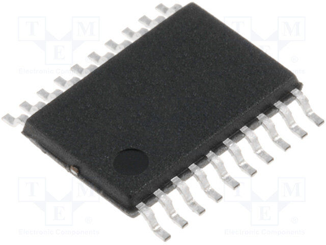
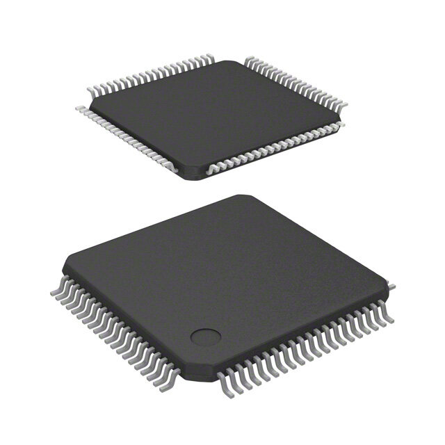
| 供应商器件封装 | 20-TSSOP |
| 其它名称 | 497-11577 |
| 其它有关文件 | http://www.st.com/web/catalog/mmc/FM141/SC1244/SS1010/LN754/PF215114?referrer=70071840 |
| 包装 | 管件 |
| 可用A/D通道 | 5 |
| 可编程输入/输出端数量 | 16 |
| 商标 | STMicroelectronics |
| 处理器系列 | STM8S |
| 外设 | 欠压检测/复位,POR,PWM,WDT |
| 安装风格 | SMD/SMT |
| 定时器数量 | 7 Timer |
| 封装 | Tube |
| 封装/外壳 | 20-TSSOP(0.173",4.40mm 宽) |
| 封装/箱体 | TSSOP-20 |
| 工作温度 | -40°C ~ 85°C |
| 工作电源电压 | 2.95 V to 5.5 V |
| 工厂包装数量 | 74 |
| 振荡器类型 | 内部 |
| 接口类型 | I2C, SPI, UART |
| 数据RAM大小 | 1 kB |
| 数据Ram类型 | RAM |
| 数据ROM大小 | 640 B |
| 数据Rom类型 | EEPROM |
| 数据总线宽度 | 8 bit |
| 数据转换器 | A/D 5x10b |
| 最大工作温度 | + 85 C |
| 最大时钟频率 | 16 MHz |
| 最小工作温度 | - 40 C |
| 标准包装 | 74 |
| 核心 | STM8 |
| 核心处理器 | STM8 |
| 核心尺寸 | 8-位 |
| 片上ADC | Yes |
| 片上DAC | Without DAC |
| 特色产品 | http://www.digikey.com/product-highlights/cn/zh/segger-microcontroller-systems-flasher-tools/3226 |
| 电压-电源(Vcc/Vdd) | 2.95 V ~ 5.5 V |
| 电源电压-最大 | 5.5 V |
| 电源电压-最小 | 2.95 V |
| 程序存储器大小 | 4 kB |
| 程序存储器类型 | Flash |
| 程序存储容量 | 4KB(4K x 8) |
| 系列 | STM8S103F2 |
| 输入/输出端数量 | 16 I/O |
| 连接性 | I²C, IrDA, LIN, SPI, UART/USART |
| 速度 | 16MHz |
| 配用 | /product-detail/zh/STM8%2F128-SK%2FRAIS/497-10593-ND/2035436 |


PDF Datasheet 数据手册内容提取
STM8S103F2 STM8S103F3 STM8S103K3 Access line, 16 MHz STM8S 8-bit MCU, up to 8 Kbytes Flash, data EEPROM,10-bit ADC, 3 timers, UART, SPI, I²C Datasheet - production data Features Core • 16 MHz advanced STM8 core with Harvard (cid:47)(cid:52)(cid:41)(cid:51)(cid:22)(cid:21) (cid:56)(cid:41)(cid:52)(cid:41)(cid:51)(cid:49)(cid:22)(cid:21) (cid:54)(cid:39)(cid:44)(cid:51)(cid:22)(cid:21)(cid:3) (cid:26)(cid:3)(cid:91)(cid:3)(cid:26)(cid:3)(cid:80)(cid:80) (cid:24)(cid:3)(cid:91)(cid:3)(cid:24)(cid:3)(cid:80)(cid:80) (cid:23)(cid:19)(cid:19)(cid:3)(cid:80)(cid:76)(cid:79)(cid:86) architecture and 3-stage pipeline • Extended instruction set Memories • Program memory: 8 Kbyte Flash; data retention 20 years at 55 °C after 10 kcycle (cid:55)(cid:54)(cid:54)(cid:50)(cid:51)(cid:21)(cid:19) (cid:54)(cid:50)(cid:21)(cid:19) (cid:56)(cid:41)(cid:52)(cid:41)(cid:51)(cid:49)(cid:21)(cid:19) • Data memory: 640 byte true data EEPROM; (cid:23)(cid:17)(cid:23)(cid:19)(cid:3)(cid:80)(cid:80)(cid:3)(cid:69)(cid:82)(cid:71)(cid:92) (cid:22)(cid:19)(cid:19)(cid:3)(cid:80)(cid:76)(cid:79)(cid:86) (cid:22)(cid:3)(cid:91)(cid:3)(cid:22)(cid:3)(cid:80)(cid:48)(cid:54)(cid:80)(cid:89)(cid:22)(cid:25)(cid:23)(cid:20)(cid:23)(cid:57)(cid:20) endurance 300 kcycle • 16-bit general purpose timer, with 3 CAPCOM • RAM: 1 Kbyte channels (IC, OC or PWM) • 8-bit basic timer with 8-bit prescaler Clock, reset and supply management • Auto wake-up timer • 2.95 to 5.5 V operating voltage • Window watchdog and independent watchdog • Flexible clock control, 4 master clock sources timers – Low power crystal resonator oscillator Communication interfaces – External clock input – Internal, user-trimmable 16 MHz RC • UART with clock output for synchronous operation, SmartCard, IrDA, LIN master mode – Internal low-power 128 kHz RC • Clock security system with clock monitor • SPI interface up to 8 Mbit/s • Power management: • I2C interface up to 400 kbit/s – Low-power modes (wait, active-halt, halt) Analog to digital converter (ADC) – Switch-off peripheral clocks individually • 10-bit, ±1 LSB ADC with up to 5 multiplexed • Permanently active, low-consumption power- channels, scan mode and analog watchdog on and power-down reset I/Os Interrupt management • Up to 28 I/Os on a 32-pin package including • Nested interrupt controller with 32 interrupts 21 high sink outputs • Up to 27 external interrupts on 6 vectors • Highly robust I/O design, immune against current injection Timers • Advanced control timer: 16-bit, 4 CAPCOM Unique ID channels, 3 complementary outputs, dead-time • 96-bit unique key for each device insertion and flexible synchronization February 2017 DocID15441 Rev 14 1/121 This is information on a product in full production. www.st.com
Contents STM8S103F2 STM8S103F3 STM8S103K3 Contents 1 Introduction . . . . . . . . . . . . . . . . . . . . . . . . . . . . . . . . . . . . . . . . . . . . . . . . 9 2 Description . . . . . . . . . . . . . . . . . . . . . . . . . . . . . . . . . . . . . . . . . . . . . . . . 10 3 Block diagram . . . . . . . . . . . . . . . . . . . . . . . . . . . . . . . . . . . . . . . . . . . . . 11 4 Product overview . . . . . . . . . . . . . . . . . . . . . . . . . . . . . . . . . . . . . . . . . . 12 4.1 Central processing unit STM8 . . . . . . . . . . . . . . . . . . . . . . . . . . . . . . . . . 12 4.2 Single wire interface module (SWIM) and debug module (DM) . . . . . . . . 13 4.3 Interrupt controller . . . . . . . . . . . . . . . . . . . . . . . . . . . . . . . . . . . . . . . . . . 13 4.4 Flash program and data EEPROM memory . . . . . . . . . . . . . . . . . . . . . . . 13 4.5 Clock controller . . . . . . . . . . . . . . . . . . . . . . . . . . . . . . . . . . . . . . . . . . . . . 15 4.6 Power management . . . . . . . . . . . . . . . . . . . . . . . . . . . . . . . . . . . . . . . . . 16 4.7 Watchdog timers . . . . . . . . . . . . . . . . . . . . . . . . . . . . . . . . . . . . . . . . . . . 16 4.8 Auto wakeup counter . . . . . . . . . . . . . . . . . . . . . . . . . . . . . . . . . . . . . . . . 17 4.9 Beeper . . . . . . . . . . . . . . . . . . . . . . . . . . . . . . . . . . . . . . . . . . . . . . . . . . . 17 4.10 TIM1 - 16-bit advanced control timer . . . . . . . . . . . . . . . . . . . . . . . . . . . . 17 4.11 TIM2 - 16-bit general purpose timer . . . . . . . . . . . . . . . . . . . . . . . . . . . . . 17 4.12 TIM4 - 8-bit basic timer . . . . . . . . . . . . . . . . . . . . . . . . . . . . . . . . . . . . . . . 18 4.13 Analog-to-digital converter (ADC1) . . . . . . . . . . . . . . . . . . . . . . . . . . . . . 18 4.14 Communication interfaces . . . . . . . . . . . . . . . . . . . . . . . . . . . . . . . . . . . . 18 4.14.1 UART1 . . . . . . . . . . . . . . . . . . . . . . . . . . . . . . . . . . . . . . . . . . . . . . . . . . 19 4.14.2 SPI . . . . . . . . . . . . . . . . . . . . . . . . . . . . . . . . . . . . . . . . . . . . . . . . . . . . . 19 4.14.3 I2C . . . . . . . . . . . . . . . . . . . . . . . . . . . . . . . . . . . . . . . . . . . . . . . . . . . . . 20 5 Pinout and pin description . . . . . . . . . . . . . . . . . . . . . . . . . . . . . . . . . . . 21 5.1 STM8S103K3 UFQFPN32/LQFP32/SDIP32 pinout and pin description . . . . . . . . . . . . . . . . . . . . . . . . . . . . . . . . . . . . . . . . . . . . . . . . 22 5.2 STM8S103F2/F3 TSSOP20/SO20/UFQFPN20 pinout and pin description . . . . . . . . . . . . . . . . . . . . . . . . . . . . . . . . . . . . . . . . . . . . . . . . 26 5.2.1 STM8S103F2/F3 TSSOP20/SO20 pinout . . . . . . . . . . . . . . . . . . . . . . . 26 5.2.2 STM8S103F2/F3 UFQFPN20 pinout . . . . . . . . . . . . . . . . . . . . . . . . . . . 27 5.3 Alternate function remapping . . . . . . . . . . . . . . . . . . . . . . . . . . . . . . . . . . 30 2/121 DocID15441 Rev 14
STM8S103F2 STM8S103F3 STM8S103K3 Contents 6 Memory and register map . . . . . . . . . . . . . . . . . . . . . . . . . . . . . . . . . . . . 31 6.1 Memory map . . . . . . . . . . . . . . . . . . . . . . . . . . . . . . . . . . . . . . . . . . . . . . 31 6.2 Register map . . . . . . . . . . . . . . . . . . . . . . . . . . . . . . . . . . . . . . . . . . . . . . 32 6.2.1 I/O port hardware register map . . . . . . . . . . . . . . . . . . . . . . . . . . . . . . . 32 6.2.2 General hardware register map . . . . . . . . . . . . . . . . . . . . . . . . . . . . . . . 33 6.2.3 CPU/SWIM/debug module/interrupt controller registers . . . . . . . . . . . . 41 7 Interrupt vector mapping . . . . . . . . . . . . . . . . . . . . . . . . . . . . . . . . . . . . 43 8 Option byte . . . . . . . . . . . . . . . . . . . . . . . . . . . . . . . . . . . . . . . . . . . . . . . 45 8.1 Alternate function remapping bits . . . . . . . . . . . . . . . . . . . . . . . . . . . . . . . 47 9 Unique ID . . . . . . . . . . . . . . . . . . . . . . . . . . . . . . . . . . . . . . . . . . . . . . . . . 49 10 Electrical characteristics . . . . . . . . . . . . . . . . . . . . . . . . . . . . . . . . . . . . 50 10.1 Parameter conditions . . . . . . . . . . . . . . . . . . . . . . . . . . . . . . . . . . . . . . . . 50 10.1.1 Minimum and maximum values . . . . . . . . . . . . . . . . . . . . . . . . . . . . . . . 50 10.1.2 Typical values . . . . . . . . . . . . . . . . . . . . . . . . . . . . . . . . . . . . . . . . . . . . 50 10.1.3 Typical curves . . . . . . . . . . . . . . . . . . . . . . . . . . . . . . . . . . . . . . . . . . . . 50 10.1.4 Loading capacitor . . . . . . . . . . . . . . . . . . . . . . . . . . . . . . . . . . . . . . . . . 50 10.1.5 Pin input voltage . . . . . . . . . . . . . . . . . . . . . . . . . . . . . . . . . . . . . . . . . . 50 10.2 Absolute maximum ratings . . . . . . . . . . . . . . . . . . . . . . . . . . . . . . . . . . . . 51 10.3 Operating conditions . . . . . . . . . . . . . . . . . . . . . . . . . . . . . . . . . . . . . . . . 52 10.3.1 VCAP external capacitor . . . . . . . . . . . . . . . . . . . . . . . . . . . . . . . . . . . . 55 10.3.2 Supply current characteristics . . . . . . . . . . . . . . . . . . . . . . . . . . . . . . . . 55 10.3.3 External clock sources and timing characteristics . . . . . . . . . . . . . . . . . 64 10.3.4 Internal clock sources and timing characteristics . . . . . . . . . . . . . . . . . 67 10.3.5 Memory characteristics . . . . . . . . . . . . . . . . . . . . . . . . . . . . . . . . . . . . . 69 10.3.6 I/O port pin characteristics . . . . . . . . . . . . . . . . . . . . . . . . . . . . . . . . . . . 70 10.3.7 Reset pin characteristics . . . . . . . . . . . . . . . . . . . . . . . . . . . . . . . . . . . . 75 10.3.8 SPI serial peripheral interface . . . . . . . . . . . . . . . . . . . . . . . . . . . . . . . . 77 10.3.9 I2C interface characteristics . . . . . . . . . . . . . . . . . . . . . . . . . . . . . . . . . . 81 10.3.10 10-bit ADC characteristics . . . . . . . . . . . . . . . . . . . . . . . . . . . . . . . . . . . 82 10.3.11 EMC characteristics . . . . . . . . . . . . . . . . . . . . . . . . . . . . . . . . . . . . . . . . 86 11 Package information . . . . . . . . . . . . . . . . . . . . . . . . . . . . . . . . . . . . . . . . 89 11.1 LQFP32 package information . . . . . . . . . . . . . . . . . . . . . . . . . . . . . . . . . . 89 DocID15441 Rev 14 3/121 4
Contents STM8S103F2 STM8S103F3 STM8S103K3 11.2 UFQFPN32 package information . . . . . . . . . . . . . . . . . . . . . . . . . . . . . . . 92 11.3 UFQFPN20 package information . . . . . . . . . . . . . . . . . . . . . . . . . . . . . . . 95 11.4 SDIP32 package information . . . . . . . . . . . . . . . . . . . . . . . . . . . . . . . . . . 98 11.5 TSSOP20 package information . . . . . . . . . . . . . . . . . . . . . . . . . . . . . . . 100 11.6 SO20 package information . . . . . . . . . . . . . . . . . . . . . . . . . . . . . . . . . . . 103 11.7 UFQFPN recommended footprint . . . . . . . . . . . . . . . . . . . . . . . . . . . . . . 104 12 Thermal characteristics . . . . . . . . . . . . . . . . . . . . . . . . . . . . . . . . . . . . 106 12.1 Reference document . . . . . . . . . . . . . . . . . . . . . . . . . . . . . . . . . . . . . . . 106 12.2 Selecting the product temperature range . . . . . . . . . . . . . . . . . . . . . . . . 107 13 Ordering information . . . . . . . . . . . . . . . . . . . . . . . . . . . . . . . . . . . . . . 108 13.1 STM8S103 FASTROM microcontroller option list . . . . . . . . . . . . . . . . . 109 14 STM8 development tools . . . . . . . . . . . . . . . . . . . . . . . . . . . . . . . . . . . 113 14.1 Emulation and in-circuit debugging tools . . . . . . . . . . . . . . . . . . . . . . . . .113 14.1.1 STice key features . . . . . . . . . . . . . . . . . . . . . . . . . . . . . . . . . . . . . . . . 113 14.2 Software tools . . . . . . . . . . . . . . . . . . . . . . . . . . . . . . . . . . . . . . . . . . . . . .114 14.2.1 STM8 toolset . . . . . . . . . . . . . . . . . . . . . . . . . . . . . . . . . . . . . . . . . . . . 114 14.2.2 C and assembly toolchains . . . . . . . . . . . . . . . . . . . . . . . . . . . . . . . . . 114 14.3 Programming tools . . . . . . . . . . . . . . . . . . . . . . . . . . . . . . . . . . . . . . . . . .115 15 Revision history . . . . . . . . . . . . . . . . . . . . . . . . . . . . . . . . . . . . . . . . . . 116 4/121 DocID15441 Rev 14
STM8S103F2 STM8S103F3 STM8S103K3 List of tables List of tables Table 1. STM8S103F2/x3 access line features . . . . . . . . . . . . . . . . . . . . . . . . . . . . . . . . . . . . . . . . 10 Table 2. Peripheral clock gating bit assignments in CLK_PCKENR1/2 registers. . . . . . . . . . . . . . . 15 Table 3. TIM timer features. . . . . . . . . . . . . . . . . . . . . . . . . . . . . . . . . . . . . . . . . . . . . . . . . . . . . . . . 18 Table 4. Legend/abbreviations for pin description tables. . . . . . . . . . . . . . . . . . . . . . . . . . . . . . . . . 21 Table 5. STM8S103K3 pin descriptions. . . . . . . . . . . . . . . . . . . . . . . . . . . . . . . . . . . . . . . . . . . . . . 23 Table 6. STM8S103F2 and STM8S103F3 pin descriptions. . . . . . . . . . . . . . . . . . . . . . . . . . . . . . . 28 Table 7. I/O port hardware register map. . . . . . . . . . . . . . . . . . . . . . . . . . . . . . . . . . . . . . . . . . . . . . 32 Table 8. General hardware register map . . . . . . . . . . . . . . . . . . . . . . . . . . . . . . . . . . . . . . . . . . . . . 33 Table 9. CPU/SWIM/debug module/interrupt controller registers. . . . . . . . . . . . . . . . . . . . . . . . . . . 41 Table 10. Interrupt mapping . . . . . . . . . . . . . . . . . . . . . . . . . . . . . . . . . . . . . . . . . . . . . . . . . . . . . . . . 43 Table 11. Option byte. . . . . . . . . . . . . . . . . . . . . . . . . . . . . . . . . . . . . . . . . . . . . . . . . . . . . . . . . . . . . 45 Table 12. Option byte description. . . . . . . . . . . . . . . . . . . . . . . . . . . . . . . . . . . . . . . . . . . . . . . . . . . . 46 Table 13. STM8S103K3 alternate function remapping bits for 32-pin devices. . . . . . . . . . . . . . . . . . 47 Table 14. STM8S103Fx alternate function remapping bits for 20-pin devices. . . . . . . . . . . . . . . . . . 48 Table 15. Unique ID registers (96 bits). . . . . . . . . . . . . . . . . . . . . . . . . . . . . . . . . . . . . . . . . . . . . . . . 49 Table 16. Voltage characteristics . . . . . . . . . . . . . . . . . . . . . . . . . . . . . . . . . . . . . . . . . . . . . . . . . . . . 51 Table 17. Current characteristics . . . . . . . . . . . . . . . . . . . . . . . . . . . . . . . . . . . . . . . . . . . . . . . . . . . . 51 Table 18. Thermal characteristics. . . . . . . . . . . . . . . . . . . . . . . . . . . . . . . . . . . . . . . . . . . . . . . . . . . . 52 Table 19. General operating conditions . . . . . . . . . . . . . . . . . . . . . . . . . . . . . . . . . . . . . . . . . . . . . . . 52 Table 20. Operating conditions at power-up/power-down . . . . . . . . . . . . . . . . . . . . . . . . . . . . . . . . . 53 Table 21. Total current consumption with code execution in run mode at V = 5 V. . . . . . . . . . . . . 55 DD Table 22. Total current consumption with code execution in run mode at V = 3.3 V . . . . . . . . . . . 56 DD Table 23. Total current consumption in wait mode at V = 5 V . . . . . . . . . . . . . . . . . . . . . . . . . . . . 57 DD Table 24. Total current consumption in wait mode at V = 3.3 V. . . . . . . . . . . . . . . . . . . . . . . . . . . 57 DD Table 25. Total current consumption in active halt mode at V = 5 V . . . . . . . . . . . . . . . . . . . . . . . 58 DD Table 26. Total current consumption in active halt mode at V = 3.3 V. . . . . . . . . . . . . . . . . . . . . . 58 DD Table 27. Total current consumption in halt mode at V = 5 V. . . . . . . . . . . . . . . . . . . . . . . . . . . . . 59 DD Table 28. Total current consumption in halt mode at V = 3.3 V . . . . . . . . . . . . . . . . . . . . . . . . . . . 59 DD Table 29. Wakeup times. . . . . . . . . . . . . . . . . . . . . . . . . . . . . . . . . . . . . . . . . . . . . . . . . . . . . . . . . . . 59 Table 30. Total current consumption and timing in forced reset state . . . . . . . . . . . . . . . . . . . . . . . . 60 Table 31. Peripheral current consumption . . . . . . . . . . . . . . . . . . . . . . . . . . . . . . . . . . . . . . . . . . . . . 60 Table 32. HSE user external clock characteristics. . . . . . . . . . . . . . . . . . . . . . . . . . . . . . . . . . . . . . . 64 Table 33. HSE oscillator characteristics. . . . . . . . . . . . . . . . . . . . . . . . . . . . . . . . . . . . . . . . . . . . . . . 65 Table 34. HSI oscillator characteristics. . . . . . . . . . . . . . . . . . . . . . . . . . . . . . . . . . . . . . . . . . . . . . . . 67 Table 35. LSI oscillator characteristics. . . . . . . . . . . . . . . . . . . . . . . . . . . . . . . . . . . . . . . . . . . . . . . . 68 Table 36. RAM and hardware registers . . . . . . . . . . . . . . . . . . . . . . . . . . . . . . . . . . . . . . . . . . . . . . . 69 Table 37. Flash program memory/data EEPROM memory . . . . . . . . . . . . . . . . . . . . . . . . . . . . . . . . 69 Table 38. I/O static characteristics . . . . . . . . . . . . . . . . . . . . . . . . . . . . . . . . . . . . . . . . . . . . . . . . . . . 70 Table 39. Output driving current (standard ports). . . . . . . . . . . . . . . . . . . . . . . . . . . . . . . . . . . . . . . . 71 Table 40. Output driving current (true open drain ports). . . . . . . . . . . . . . . . . . . . . . . . . . . . . . . . . . . 72 Table 41. Output driving current (high sink ports). . . . . . . . . . . . . . . . . . . . . . . . . . . . . . . . . . . . . . . . 72 Table 42. NRST pin characteristics . . . . . . . . . . . . . . . . . . . . . . . . . . . . . . . . . . . . . . . . . . . . . . . . . . 75 Table 43. SPI characteristics . . . . . . . . . . . . . . . . . . . . . . . . . . . . . . . . . . . . . . . . . . . . . . . . . . . . . . . 77 Table 44. I2C characteristics. . . . . . . . . . . . . . . . . . . . . . . . . . . . . . . . . . . . . . . . . . . . . . . . . . . . . . . . 81 Table 45. ADC characteristics . . . . . . . . . . . . . . . . . . . . . . . . . . . . . . . . . . . . . . . . . . . . . . . . . . . . . . 82 Table 46. ADC accuracy with R < 10 kΩ, V = 5 V . . . . . . . . . . . . . . . . . . . . . . . . . . . . . . . . . . . . 83 AIN DD Table 47. ADC accuracy with R < 10 kΩ, V = 3.3 V. . . . . . . . . . . . . . . . . . . . . . . . . . . . . . . . . . . 84 AIN DD Table 48. EMS data . . . . . . . . . . . . . . . . . . . . . . . . . . . . . . . . . . . . . . . . . . . . . . . . . . . . . . . . . . . . . . 86 DocID15441 Rev 14 5/121 6
List of tables STM8S103F2 STM8S103F3 STM8S103K3 Table 49. EMI data. . . . . . . . . . . . . . . . . . . . . . . . . . . . . . . . . . . . . . . . . . . . . . . . . . . . . . . . . . . . . . . 87 Table 50. ESD absolute maximum ratings. . . . . . . . . . . . . . . . . . . . . . . . . . . . . . . . . . . . . . . . . . . . . 87 Table 51. Electrical sensitivities . . . . . . . . . . . . . . . . . . . . . . . . . . . . . . . . . . . . . . . . . . . . . . . . . . . . . 88 Table 52. LQFP32 - 32-pin, 7 x 7 mm low-profile quad flat package mechanical data. . . . . . . . . . . . 90 Table 53. UFQFPN32 - 32-pin, 5x5 mm, 0.5 mm pitch ultra thin fine pitch quad flat package mechanical data. . . . . . . . . . . . . . . . . . . . . . . . . . . . . . . . . . . . . . . . . . . . . . . . . . 93 Table 54. UFQFPN20 - 20-lead, 3x3 mm, 0.5 mm pitch, ultra thin fine pitch quad flat package mechanical data. . . . . . . . . . . . . . . . . . . . . . . . . . . . . . . . . . . . . . . . . . . . . . . . . . 95 Table 55. SDIP32 package mechanical data . . . . . . . . . . . . . . . . . . . . . . . . . . . . . . . . . . . . . . . . . . . 98 Table 56. TSSOP20 package mechanical data . . . . . . . . . . . . . . . . . . . . . . . . . . . . . . . . . . . . . . . . 100 Table 57. SO20 mechanical data. . . . . . . . . . . . . . . . . . . . . . . . . . . . . . . . . . . . . . . . . . . . . . . . . . . 103 Table 58. Thermal characteristics. . . . . . . . . . . . . . . . . . . . . . . . . . . . . . . . . . . . . . . . . . . . . . . . . . . 106 Table 59. Document revision history . . . . . . . . . . . . . . . . . . . . . . . . . . . . . . . . . . . . . . . . . . . . . . . . 116 6/121 DocID15441 Rev 14
STM8S103F2 STM8S103F3 STM8S103K3 List of figures List of figures Figure 1. STM8S103F2/x3 block diagram . . . . . . . . . . . . . . . . . . . . . . . . . . . . . . . . . . . . . . . . . . . . 11 Figure 2. Flash memory organization . . . . . . . . . . . . . . . . . . . . . . . . . . . . . . . . . . . . . . . . . . . . . . . . 14 Figure 3. STM8S103K3 UFQFPN32/LQFP32 pinout . . . . . . . . . . . . . . . . . . . . . . . . . . . . . . . . . . . . 22 Figure 4. STM8S103K3 SDIP32 pinout. . . . . . . . . . . . . . . . . . . . . . . . . . . . . . . . . . . . . . . . . . . . . . . 23 Figure 5. STM8S103F2/F3 TSSOP20/SO20 pinout . . . . . . . . . . . . . . . . . . . . . . . . . . . . . . . . . . . . . 26 Figure 6. STM8S103F2/F3 UFQFPN20-pin pinout . . . . . . . . . . . . . . . . . . . . . . . . . . . . . . . . . . . . . . 27 Figure 7. Memory map . . . . . . . . . . . . . . . . . . . . . . . . . . . . . . . . . . . . . . . . . . . . . . . . . . . . . . . . . . . 31 Figure 8. Pin loading conditions. . . . . . . . . . . . . . . . . . . . . . . . . . . . . . . . . . . . . . . . . . . . . . . . . . . . . 50 Figure 9. Pin input voltage. . . . . . . . . . . . . . . . . . . . . . . . . . . . . . . . . . . . . . . . . . . . . . . . . . . . . . . . . 51 Figure 10. f versus V . . . . . . . . . . . . . . . . . . . . . . . . . . . . . . . . . . . . . . . . . . . . . . . . . . . . . . 53 CPUmax DD Figure 11. External capacitor C . . . . . . . . . . . . . . . . . . . . . . . . . . . . . . . . . . . . . . . . . . . . . . . . . . . 55 EXT Figure 12. Typ I vs. V HSE user external clock, f = 16 MHz . . . . . . . . . . . . . . . . . . . . 61 DD(RUN) DD CPU Figure 13. Typ I vs. f HSE user external clock, V = 5 V . . . . . . . . . . . . . . . . . . . . . . . . 61 DD(RUN) CPU DD Figure 14. Typ I vs. V HSI RC osc, f = 16 MHz . . . . . . . . . . . . . . . . . . . . . . . . . . . . . . 62 DD(RUN) DD CPU Figure 15. Typ I vs. V HSE external clock, f = 16 MHz . . . . . . . . . . . . . . . . . . . . . . . . . 62 DD(WFI) DD CPU Figure 16. Typ I vs. f HSE external clock, V = 5 V . . . . . . . . . . . . . . . . . . . . . . . . . . . . 63 DD(WFI) CPU DD Figure 17. Typ I vs. V HSI RC osc., f = 16 MHz . . . . . . . . . . . . . . . . . . . . . . . . . . . . . . 63 DD(WFI) DD CPU Figure 18. HSE external clock source . . . . . . . . . . . . . . . . . . . . . . . . . . . . . . . . . . . . . . . . . . . . . . . . . 64 Figure 19. HSE oscillator circuit diagram. . . . . . . . . . . . . . . . . . . . . . . . . . . . . . . . . . . . . . . . . . . . . . . 66 Figure 20. Typical HSI frequency variation vs V @ 4 temperatures . . . . . . . . . . . . . . . . . . . . . . . . 67 DD Figure 21. Typical LSI frequency variation vs V @ 4 temperatures . . . . . . . . . . . . . . . . . . . . . . . . . 68 DD Figure 22. Typical V and V vs V @ 4 temperatures. . . . . . . . . . . . . . . . . . . . . . . . . . . . . . . . . . 71 IL IH DD Figure 23. Typical pull-up current vs V @ 4 temperatures . . . . . . . . . . . . . . . . . . . . . . . . . . . . . . . 71 DD Figure 24. Typical pull-up resistance vs VDD @ 4 temperatures . . . . . . . . . . . . . . . . . . . . . . . . . . . . 71 Figure 25. Typ. V @ V = 3.3 V (standard ports) . . . . . . . . . . . . . . . . . . . . . . . . . . . . . . . . . . . . . 72 OL DD Figure 26. Typ. V @ V = 5.0 V (standard ports) . . . . . . . . . . . . . . . . . . . . . . . . . . . . . . . . . . . . . 72 OL DD Figure 27. Typ. V @ V = 3.3 V (true open drain ports) . . . . . . . . . . . . . . . . . . . . . . . . . . . . . . . . 73 OL DD Figure 28. Typ. V @ V = 5.0 V (true open drain ports) . . . . . . . . . . . . . . . . . . . . . . . . . . . . . . . . 73 OL DD Figure 29. Typ. V @ V = 3.3 V (high sink ports) . . . . . . . . . . . . . . . . . . . . . . . . . . . . . . . . . . . . . 73 OL DD Figure 30. Typ. V @ V = 5.0 V (high sink ports) . . . . . . . . . . . . . . . . . . . . . . . . . . . . . . . . . . . . . 73 OL DD Figure 31. Typ. V - V @ V = 3.3 V (standard ports) . . . . . . . . . . . . . . . . . . . . . . . . . . . . . . . . 74 DD OH DD Figure 32. Typ. V - V @ V = 5.0 V (standard ports) . . . . . . . . . . . . . . . . . . . . . . . . . . . . . . . . 74 DD OH DD Figure 33. Typ. V - V @ V = 3.3 V (high sink ports) . . . . . . . . . . . . . . . . . . . . . . . . . . . . . . . . 74 DD OH DD Figure 34. Typ. V - V @ V = 5.0 V (high sink ports) . . . . . . . . . . . . . . . . . . . . . . . . . . . . . . . . 74 DD OH DD Figure 35. Typical NRST V and V vs V @ 4 temperatures. . . . . . . . . . . . . . . . . . . . . . . . . . . . . 75 IL IH DD Figure 36. Typical NRST pull-up resistance R vs V @ 4 temperatures. . . . . . . . . . . . . . . . . . . . 76 PU DD Figure 37. Typical NRST pull-up current I vs V @ 4 temperatures. . . . . . . . . . . . . . . . . . . . . . . . 76 pu DD Figure 38. Recommended reset pin protection . . . . . . . . . . . . . . . . . . . . . . . . . . . . . . . . . . . . . . . . . . 77 Figure 39. SPI timing diagram where slave mode and CPHA = 0. . . . . . . . . . . . . . . . . . . . . . . . . . . . 79 Figure 40. SPI timing diagram where slave mode and CPHA = 1. . . . . . . . . . . . . . . . . . . . . . . . . . . . 79 Figure 41. SPI timing diagram - master mode. . . . . . . . . . . . . . . . . . . . . . . . . . . . . . . . . . . . . . . . . . . 80 Figure 42. Typical application with I2C bus and timing diagram . . . . . . . . . . . . . . . . . . . . . . . . . . . . . 81 Figure 43. ADC accuracy characteristics. . . . . . . . . . . . . . . . . . . . . . . . . . . . . . . . . . . . . . . . . . . . . . . 84 Figure 44. Typical application with ADC . . . . . . . . . . . . . . . . . . . . . . . . . . . . . . . . . . . . . . . . . . . . . . . 85 Figure 45. LQFP32 - 32-pin, 7 x 7 mm low-profile quad flat package outline . . . . . . . . . . . . . . . . . . . 89 Figure 46. LQFP32 - 32-pin, 7 x 7 mm low-profile quad flat package recommended footprint . . . . . . 90 Figure 47. LQFP32 marking example (package top view) . . . . . . . . . . . . . . . . . . . . . . . . . . . . . . . . . 91 Figure 48. UFQFPN32 - 32-pin, 5x5 mm, 0.5 mm pitch ultra thin fine pitch quad flat DocID15441 Rev 14 7/121 8
List of figures STM8S103F2 STM8S103F3 STM8S103K3 package outline. . . . . . . . . . . . . . . . . . . . . . . . . . . . . . . . . . . . . . . . . . . . . . . . . . . . . . . . . . 92 Figure 49. UFQFPN32 - 32-pin, 5 x5 mm, 0.5 mm pitch ultra thin fine pitch quad flat package recommended footprint . . . . . . . . . . . . . . . . . . . . . . . . . . . . . . . . . . . . . . . . . . . . 93 Figure 50. UFQFPN32 marking example (package top view) . . . . . . . . . . . . . . . . . . . . . . . . . . . . . . 94 Figure 51. UFQFPN20 - 20-lead, 3x3 mm, 0.5 mm pitch, ultra thin fine pitch quad flat package outline. . . . . . . . . . . . . . . . . . . . . . . . . . . . . . . . . . . . . . . . . . . . . . . . . . . . . . . . . . 95 Figure 52. UFQFPN20 - 20-lead, 3x3 mm, 0.5 mm pitch, ultra thin fine pitch quad flat package recommended footprint . . . . . . . . . . . . . . . . . . . . . . . . . . . . . . . . . . . . . . . . . . . . 96 Figure 53. UFQFPN20 marking example (package top view) . . . . . . . . . . . . . . . . . . . . . . . . . . . . . . . 97 Figure 54. SDIP32 package outline. . . . . . . . . . . . . . . . . . . . . . . . . . . . . . . . . . . . . . . . . . . . . . . . . . . 98 Figure 55. SDIP32 marking example (package top view) . . . . . . . . . . . . . . . . . . . . . . . . . . . . . . . . . 99 Figure 56. TSSOP20 package outline. . . . . . . . . . . . . . . . . . . . . . . . . . . . . . . . . . . . . . . . . . . . . . . . 100 Figure 57. TSSOP20 recommended package footprint. . . . . . . . . . . . . . . . . . . . . . . . . . . . . . . . . . . 101 Figure 58. TSSOP20 marking example (package top view) . . . . . . . . . . . . . . . . . . . . . . . . . . . . . . . 102 Figure 59. SO20 package outline . . . . . . . . . . . . . . . . . . . . . . . . . . . . . . . . . . . . . . . . . . . . . . . . . . . 103 Figure 60. SO20 marking example (package top view) . . . . . . . . . . . . . . . . . . . . . . . . . . . . . . . . . . 104 Figure 61. UFQFPN recommended footprint for on-board emulation . . . . . . . . . . . . . . . . . . . . . . . . 104 Figure 62. UFQFPN recommended footprint without on-board emulation. . . . . . . . . . . . . . . . . . . . . 105 Figure 63. STM8S103F2/x3 access line ordering information scheme(1) . . . . . . . . . . . . . . . . . . . . . 108 8/121 DocID15441 Rev 14
STM8S103F2 STM8S103F3 STM8S103K3 Introduction 1 Introduction This datasheet contains the description of the device features, pinout, electrical characteristics, mechanical data and ordering information. • For complete information on the STM8S microcontroller memory, registers and peripherals, please refer to the STM8S microcontroller family reference manual (RM0016). • For information on programming, erasing and protection of the internal Flash memory please refer to the STM8S Flash programming manual (PM0051). • For information on the debug and SWIM (single wire interface module) refer to the STM8 SWIM communication protocol and debug module user manual (UM0470). • For information on the STM8 core, please refer to the STM8 CPU programming manual (PM0044). DocID15441 Rev 14 9/121 20
Description STM8S103F2 STM8S103F3 STM8S103K3 2 Description The STM8S103F2/x3 access line 8-bit microcontrollers offer 8 Kbyte Flash program memory, plus integrated true data EEPROM. The STM8S microcontroller family reference manual (RM0016) refers to devices in this family as low-density. They provide the following benefits: performance, robustness, and reduced system cost. Device performance and robustness are ensured by advanced core and peripherals made in a state-of-the art technology, a 16 MHz clock frequency, robust I/Os, independent watchdogs with separate clock source, and a clock security system. The system cost is reduced thanks to an integrated true data EEPROM for up to 300 k write/erase cycles and a high system integration level with internal clock oscillators, watchdog and brown-out reset. Full documentation is offered as well as a wide choice of development tools. Table 1. STM8S103F2/x3 access line features Device STM8S103K3 STM8S103F3 STM8S103F2 Pin count 32 20 20 Maximum number of 28 16 16 GPIOs (I/Os) Ext. interrupt pins 27 16 16 Timer CAPCOM 7 7 7 channels Timer complementary 3 2 2 outputs A/D converter channels 4 5 5 High sink I/Os 21 12 12 Low density Flash program memory 8K 8K 4K (bytes) Data EEPROM (bytes) 640(1) 640(1) 640(1) RAM (bytes) 1K 1K 1K Multipurpose timer (TIM1), SPI, I2C, UART window WDG, independent Peripheral set WDG, ADC, PWM timer (TIM2), 8-bit timer (TIM4) 1. No read-while-write (RWW) capability. 10/121 DocID15441 Rev 14
STM8S103F2 STM8S103F3 STM8S103K3 Block diagram 3 Block diagram Figure 1. STM8S103F2/x3 block diagram (cid:53)(cid:72)(cid:86)(cid:72)(cid:87)(cid:3)(cid:69)(cid:79)(cid:82)(cid:70)(cid:78) (cid:59)(cid:55)(cid:36)(cid:47)(cid:3)(cid:20)(cid:16)(cid:20)(cid:25)(cid:3)(cid:48)(cid:43)(cid:93) (cid:38)(cid:79)(cid:82)(cid:70)(cid:78)(cid:3)(cid:70)(cid:82)(cid:81)(cid:87)(cid:85)(cid:82)(cid:79)(cid:79)(cid:72)(cid:85) (cid:53)(cid:72)(cid:86)(cid:72)(cid:87) (cid:53)(cid:72)(cid:86)(cid:72)(cid:87) (cid:53)(cid:38)(cid:3)(cid:76)(cid:81)(cid:87)(cid:17)(cid:3)(cid:20)(cid:25)(cid:3)(cid:48)(cid:43)(cid:93) (cid:39)(cid:72)(cid:87)(cid:72)(cid:70)(cid:87)(cid:82)(cid:85) (cid:51)(cid:50)(cid:53) (cid:37)(cid:50)(cid:53) (cid:53)(cid:38)(cid:3)(cid:76)(cid:81)(cid:87)(cid:17)(cid:3)(cid:20)(cid:21)(cid:27)(cid:3)(cid:78)(cid:43)(cid:93) (cid:38)(cid:79)(cid:82)(cid:70)(cid:78)(cid:3)(cid:87)(cid:82)(cid:3)(cid:83)(cid:72)(cid:85)(cid:76)(cid:83)(cid:75)(cid:72)(cid:85)(cid:68)(cid:79)(cid:86)(cid:3)(cid:68)(cid:81)(cid:71)(cid:3)(cid:70)(cid:82)(cid:85)(cid:72) (cid:58)(cid:76)(cid:81)(cid:71)(cid:82)(cid:90) (cid:54)(cid:55)(cid:48)(cid:27)(cid:3) (cid:58)(cid:39)(cid:42) (cid:70)(cid:82)(cid:85)(cid:72) (cid:44)(cid:81)(cid:71)(cid:72)(cid:83)(cid:72)(cid:81)(cid:71)(cid:72)(cid:81)(cid:87)(cid:3)(cid:58)(cid:39)(cid:42) (cid:54)(cid:76)(cid:81)(cid:74)(cid:79)(cid:72)(cid:3)(cid:90)(cid:76)(cid:85)(cid:72) (cid:39)(cid:72)(cid:69)(cid:88)(cid:74)(cid:18)(cid:54)(cid:58)(cid:44)(cid:48) (cid:27)(cid:3)(cid:46)(cid:69)(cid:92)(cid:87)(cid:72)(cid:86) (cid:71)(cid:72)(cid:69)(cid:88)(cid:74)(cid:3)(cid:76)(cid:81)(cid:87)(cid:72)(cid:85)(cid:73)(cid:17) (cid:51)(cid:85)(cid:82)(cid:74)(cid:85)(cid:68)(cid:80) (cid:41)(cid:79)(cid:68)(cid:86)(cid:75) (cid:25)(cid:23)(cid:19)(cid:3)(cid:69)(cid:92)(cid:87)(cid:72)(cid:86) (cid:71)(cid:68)(cid:87)(cid:68)(cid:3)(cid:40)(cid:40)(cid:51)(cid:53)(cid:50)(cid:48) (cid:86) (cid:88) (cid:69) (cid:23)(cid:19)(cid:19)(cid:3)(cid:46)(cid:69)(cid:76)(cid:87)(cid:18)(cid:86) (cid:44)(cid:21)(cid:38) (cid:68)(cid:3) (cid:20)(cid:3)(cid:46)(cid:69)(cid:92)(cid:87)(cid:72) (cid:68)(cid:87) (cid:53)(cid:36)(cid:48) (cid:71) (cid:71)(cid:3) (cid:81) (cid:68) (cid:86)(cid:3) (cid:27)(cid:3)(cid:48)(cid:69)(cid:76)(cid:87)(cid:18)(cid:86) (cid:54)(cid:51)(cid:44) (cid:86) (cid:72) (cid:71)(cid:85) (cid:71) (cid:36) (cid:56)(cid:83)(cid:3)(cid:87)(cid:82)(cid:3)(cid:23)(cid:3)(cid:38)(cid:36)(cid:51)(cid:38)(cid:50)(cid:48)(cid:3) (cid:20)(cid:25)(cid:16)(cid:69)(cid:76)(cid:87)(cid:3)(cid:68)(cid:71)(cid:89)(cid:68)(cid:81)(cid:70)(cid:72)(cid:71) (cid:70)(cid:75)(cid:68)(cid:81)(cid:81)(cid:72)(cid:79)(cid:86)(cid:3)(cid:14)(cid:3)(cid:22)(cid:3) (cid:47)(cid:44)(cid:49)(cid:3)(cid:80)(cid:68)(cid:86)(cid:87)(cid:72)(cid:85) (cid:54)(cid:51)(cid:44)(cid:3)(cid:72)(cid:80)(cid:88)(cid:79)(cid:17) (cid:56)(cid:36)(cid:53)(cid:55)(cid:20) (cid:70)(cid:82)(cid:81)(cid:87)(cid:85)(cid:82)(cid:79)(cid:3)(cid:87)(cid:76)(cid:80)(cid:72)(cid:85)(cid:3)(cid:11)(cid:55)(cid:48)(cid:20)(cid:12)(cid:3)(cid:3) (cid:70)(cid:82)(cid:80)(cid:83)(cid:79)(cid:72)(cid:80)(cid:72)(cid:81)(cid:87)(cid:68)(cid:85)(cid:92)(cid:3) (cid:82)(cid:88)(cid:87)(cid:83)(cid:88)(cid:87)(cid:86) (cid:20)(cid:25)(cid:16)(cid:69)(cid:76)(cid:87)(cid:3)(cid:74)(cid:72)(cid:81)(cid:72)(cid:85)(cid:68)(cid:79)(cid:3)(cid:83)(cid:88)(cid:85)(cid:83)(cid:82)(cid:86)(cid:72) (cid:56)(cid:83)(cid:3)(cid:87)(cid:82)(cid:3)(cid:22)(cid:3)(cid:38)(cid:36)(cid:51)(cid:38)(cid:50)(cid:48) (cid:55)(cid:76)(cid:80)(cid:72)(cid:85)(cid:3)(cid:11)(cid:55)(cid:44)(cid:48)(cid:21)(cid:12) (cid:70)(cid:75)(cid:68)(cid:81)(cid:81)(cid:72)(cid:79)(cid:86) (cid:27)(cid:16)(cid:69)(cid:76)(cid:87)(cid:3)(cid:69)(cid:68)(cid:86)(cid:76)(cid:70)(cid:3)(cid:87)(cid:76)(cid:80)(cid:72)(cid:85) (cid:56)(cid:83)(cid:3)(cid:87)(cid:82)(cid:3)(cid:24) (cid:36)(cid:39)(cid:38)(cid:20) (cid:11)(cid:55)(cid:44)(cid:48)(cid:23)(cid:12) (cid:70)(cid:75)(cid:68)(cid:81)(cid:81)(cid:72)(cid:79)(cid:86) (cid:20)(cid:18)(cid:21)(cid:18)(cid:23)(cid:3)(cid:78)(cid:43)(cid:93) (cid:36)(cid:58)(cid:56)(cid:3)(cid:87)(cid:76)(cid:80)(cid:72)(cid:85) (cid:37)(cid:72)(cid:72)(cid:83)(cid:72)(cid:85) (cid:69)(cid:72)(cid:72)(cid:83) (cid:48)(cid:54)(cid:89)(cid:22)(cid:25)(cid:23)(cid:20)(cid:22)(cid:57)(cid:20) DocID15441 Rev 14 11/121 20
Product overview STM8S103F2 STM8S103F3 STM8S103K3 4 Product overview The following section provides an overview of the basic features of the device functional modules and peripherals. For more detailed information please refer to the corresponding family reference manual (RM0016). 4.1 Central processing unit STM8 The 8-bit STM8 core is designed for code efficiency and performance. It contains 6 internal registers which are directly addressable in each execution context, 20 addressing modes including indexed indirect and relative addressing and 80 instructions. Architecture and registers • Harvard architecture, • 3-stage pipeline, • 32-bit wide program memory bus - single cycle fetching for most instructions, • X and Y 16-bit index registers - enabling indexed addressing modes with or without offset and read-modify-write type data manipulations, • 8-bit accumulator, • 24-bit program counter - 16-Mbyte linear memory space, • 16-bit stack pointer - access to a 64 K-level stack, • 8-bit condition code register - 7 condition flags for the result of the last instruction. Addressing • 20 addressing modes, • Indexed indirect addressing mode for look-up tables located anywhere in the address space, • Stack pointer relative addressing mode for local variables and parameter passing. Instruction set • 80 instructions with 2-byte average instruction size, • Standard data movement and logic/arithmetic functions, • 8-bit by 8-bit multiplication, • 16-bit by 8-bit and 16-bit by 16-bit division, • Bit manipulation, • Data transfer between stack and accumulator (push/pop) with direct stack access, • Data transfer using the X and Y registers or direct memory-to-memory transfers. 12/121 DocID15441 Rev 14
STM8S103F2 STM8S103F3 STM8S103K3 Product overview 4.2 Single wire interface module (SWIM) and debug module (DM) The single wire interface module and debug module permits non-intrusive, real-time in- circuit debugging and fast memory programming. SWIM Single wire interface module for direct access to the debug module and memory programming. The interface can be activated in all device operation modes. The maximum data transmission speed is 145 bytes/ms. Debug module The non-intrusive debugging module features a performance close to a full-featured emulator. Beside memory and peripherals, also CPU operation can be monitored in real- time by means of shadow registers. • R/W to RAM and peripheral registers in real-time • R/W access to all resources by stalling the CPU • Breakpoints on all program-memory instructions (software breakpoints) • Two advanced breakpoints, 23 predefined configurations 4.3 Interrupt controller • Nested interrupts with three software priority levels, • 32 interrupt vectors with hardware priority, • Up to 27 external interrupts on 6 vectors including TLI, • Trap and reset interrupts 4.4 Flash program and data EEPROM memory • 8 Kbyte of Flash program single voltage Flash memory, • 640 byte true data EEPROM, • User option byte area. Write protection (WP) Write protection of Flash program memory and data EEPROM is provided to avoid unintentional overwriting of memory that could result from a user software malfunction. There are two levels of write protection. The first level is known as MASS (memory access security system). MASS is always enabled and protects the main Flash program memory, data EEPROM and option bytes. To perform in-application programming (IAP), this write protection can be removed by writing a MASS key sequence in a control register. This allows the application to write to data EEPROM, modify the contents of main program memory or the device option bytes. A second level of write protection, can be enabled to further protect a specific area of memory known as UBC (user boot code). Refer to the figure below. The size of the UBC is programmable through the UBC option byte, in increments of 1 page (64-byte block) by programming the UBC option byte in ICP mode. DocID15441 Rev 14 13/121 20
Product overview STM8S103F2 STM8S103F3 STM8S103K3 This divides the program memory into two areas: • Main program memory: up to 8 Kbyte minus UBC • User-specific boot code (UBC): Configurable up to 8 Kbyte The UBC area remains write-protected during in-application programming. This means that the MASS keys do not unlock the UBC area. It protects the memory used to store the boot program, specific code libraries, reset and interrupt vectors, the reset routine and usually the IAP and communication routines. Figure 2. Flash memory organization (cid:39)(cid:68)(cid:87)(cid:68)(cid:3)(cid:80)(cid:72)(cid:80)(cid:82)(cid:85)(cid:92)(cid:3)(cid:68)(cid:85)(cid:72)(cid:68)(cid:3)(cid:11)(cid:3)(cid:25)(cid:23)(cid:19)(cid:3)(cid:69)(cid:92)(cid:87)(cid:72)(cid:86)(cid:12) (cid:39)(cid:68)(cid:87)(cid:68) (cid:40)(cid:40)(cid:51)(cid:53)(cid:50)(cid:48) (cid:80)(cid:72)(cid:80)(cid:82)(cid:85)(cid:92) (cid:50)(cid:83)(cid:87)(cid:76)(cid:82)(cid:81)(cid:3)(cid:69)(cid:92)(cid:87)(cid:72)(cid:86) (cid:51)(cid:85)(cid:82)(cid:74)(cid:85)(cid:68)(cid:80)(cid:80)(cid:68)(cid:69)(cid:79)(cid:72)(cid:3)(cid:68)(cid:85)(cid:72)(cid:68)(cid:3) (cid:56)(cid:37)(cid:38)(cid:3)(cid:68)(cid:85)(cid:72)(cid:68) (cid:73)(cid:85)(cid:82)(cid:80)(cid:3)(cid:25)(cid:23)(cid:3)(cid:69)(cid:92)(cid:87)(cid:72)(cid:86)(cid:3) (cid:53)(cid:72)(cid:80)(cid:68)(cid:76)(cid:81)(cid:86)(cid:3)(cid:90)(cid:85)(cid:76)(cid:87)(cid:72)(cid:3)(cid:83)(cid:85)(cid:82)(cid:87)(cid:72)(cid:70)(cid:87)(cid:72)(cid:71)(cid:3)(cid:71)(cid:88)(cid:85)(cid:76)(cid:81)(cid:74)(cid:3)(cid:44)(cid:36)(cid:51) (cid:11)(cid:20)(cid:3)(cid:83)(cid:68)(cid:74)(cid:72)(cid:12)(cid:3)(cid:88)(cid:83)(cid:3)(cid:87)(cid:82)(cid:3)(cid:27)(cid:3)(cid:46)(cid:69)(cid:92)(cid:87)(cid:72)(cid:86)(cid:3) (cid:11)(cid:76)(cid:81)(cid:3)(cid:20)(cid:3)(cid:83)(cid:68)(cid:74)(cid:72)(cid:3)(cid:86)(cid:87)(cid:72)(cid:83)(cid:86)(cid:12) (cid:47)(cid:82)(cid:90)(cid:3)(cid:71)(cid:72)(cid:81)(cid:86)(cid:76)(cid:87)(cid:92)(cid:3) (cid:41)(cid:79)(cid:68)(cid:86)(cid:75)(cid:3)(cid:83)(cid:85)(cid:82)(cid:74)(cid:85)(cid:68)(cid:80)(cid:3) (cid:80)(cid:72)(cid:80)(cid:82)(cid:85)(cid:92)(cid:3)(cid:11)(cid:27)(cid:3) (cid:46)(cid:69)(cid:92)(cid:87)(cid:72)(cid:86)(cid:12) (cid:51)(cid:85)(cid:82)(cid:74)(cid:85)(cid:68)(cid:80)(cid:3)(cid:80)(cid:72)(cid:80)(cid:82)(cid:85)(cid:92)(cid:3)(cid:68)(cid:85)(cid:72)(cid:68)(cid:3) (cid:58)(cid:85)(cid:76)(cid:87)(cid:72)(cid:3)(cid:68)(cid:70)(cid:70)(cid:72)(cid:86)(cid:86)(cid:3)(cid:83)(cid:82)(cid:86)(cid:86)(cid:76)(cid:69)(cid:79)(cid:72)(cid:3)(cid:73)(cid:82)(cid:85)(cid:3)(cid:44)(cid:36)(cid:51) (cid:48)(cid:54)(cid:89)(cid:22)(cid:25)(cid:23)(cid:26)(cid:28)(cid:57)(cid:20) Read-out protection (ROP) The read-out protection blocks reading and writing the Flash program memory and data EEPROM memory in ICP mode (and debug mode). Once the read-out protection is activated, any attempt to toggle its status triggers a global erase of the program and data memory. Even if no protection can be considered as totally unbreakable, the feature provides a very high level of protection for a general purpose microcontroller. 14/121 DocID15441 Rev 14
STM8S103F2 STM8S103F3 STM8S103K3 Product overview 4.5 Clock controller The clock controller distributes the system clock (fMASTER) coming from different oscillators to the core and the peripherals. It also manages clock gating for low power modes and ensures clock robustness. Features • Clock prescaler: to get the best compromise between speed and current consumption the clock frequency to the CPU and peripherals can be adjusted by a programmable prescaler. • Safe clock switching: clock sources can be changed safely on the fly in run mode through a configuration register. The clock signal is not switched until the new clock source is ready. The design guarantees glitch-free switching. • Clock management: to reduce power consumption, the clock controller can stop the clock to the core, individual peripherals or memory. • Master clock sources: four different clock sources can be used to drive the master clock: – 1-16 MHz high-speed external crystal (HSE) – Up to 16 MHz high-speed user-external clock (HSE user-ext) – 16 MHz high-speed internal RC oscillator (HSI) – 128 kHz low-speed internal RC (LSI) • Startup clock: After reset, the microcontroller restarts by default with an internal 2 MHz clock (HSI/8). The prescaler ratio and clock source can be changed by the application program as soon as the code execution starts. • Clock security system (CSS): This feature can be enabled by software. If an HSE clock failure occurs, the internal RC (16 MHz/8) is automatically selected by the CSS and an interrupt can optionally be generated. • Configurable main clock output (CCO): This outputs an external clock for use by the application. Tab l e 2. Peripheral clock gating bit assignments in CLK_PCKENR1/2 registers Peripheral Peripheral Peripheral Peripheral Bit Bit Bit Bit clock clock clock clock PCKEN17 TIM1 PCKEN13 UART1 PCKEN27 Reserved PCKEN23 ADC PCKEN16 Reserved PCKEN12 Reserved PCKEN26 Reserved PCKEN22 AWU PCKEN15 TIM2 PCKEN11 SPI PCKEN25 Reserved PCKEN21 Reserved PCKEN14 TIM4 PCKEN10 I2C PCKEN24 Reserved PCKEN20 Reserved DocID15441 Rev 14 15/121 20
Product overview STM8S103F2 STM8S103F3 STM8S103K3 4.6 Power management For efficient power management, the application can be put in one of four different low- power modes. You can configure each mode to obtain the best compromise between lowest power consumption, fastest start-up time and available wakeup sources. • Wait mode: In this mode, the CPU is stopped, but peripherals are kept running. The wakeup is performed by an internal or external interrupt or reset. • Active halt mode with regulator on: In this mode, the CPU and peripheral clocks are stopped. An internal wakeup is generated at programmable intervals by the auto wake up unit (AWU). The main voltage regulator is kept powered on, so current consumption is higher than in active halt mode with regulator off, but the wakeup time is faster. Wakeup is triggered by the internal AWU interrupt, external interrupt or reset. • Active halt mode with regulator off: This mode is the same as active halt with regulator on, except that the main voltage regulator is powered off, so the wake up time is slower. • Halt mode: In this mode the microcontroller uses the least power. The CPU and peripheral clocks are stopped, the main voltage regulator is powered off. Wakeup is triggered by external event or reset. 4.7 Watchdog timers The watchdog system is based on two independent timers providing maximum security to the applications. Activation of the watchdog timers is controlled by option bytes or by software. Once activated, the watchdogs cannot be disabled by the user program without performing a reset. Window watchdog timer The window watchdog is used to detect the occurrence of a software fault, usually generated by external interferences or by unexpected logical conditions, which cause the application program to abandon its normal sequence. The window function can be used to trim the watchdog behavior to match the application perfectly. The application software must refresh the counter before time-out and during a limited time window. A reset is generated in two situations: 1. Timeout: At 16 MHz CPU clock the time-out period can be adjusted between 75 µs up to 64 ms. 2. Refresh out of window: The downcounter is refreshed before its value is lower than the one stored in the window register. 16/121 DocID15441 Rev 14
STM8S103F2 STM8S103F3 STM8S103K3 Product overview Independent watchdog timer The independent watchdog peripheral can be used to resolve processor malfunctions due to hardware or software failures. It is clocked by the 128 kHz LSI internal RC clock source, and thus stays active even in case of a CPU clock failure The IWDG time base spans from 60 µs to 1 s. 4.8 Auto wakeup counter • Used for auto wakeup from active halt mode, • Clock source: Internal 128 kHz internal low frequency RC oscillator or external clock, • LSI clock can be internally connected to TIM1 input capture channel 1 for calibration. 4.9 Beeper The beeper function outputs a signal on the BEEP pin for sound generation. The signal is in the range of 1, 2 or 4 kHz. The beeper output port is only available through the alternate function remap option bit AFR7. 4.10 TIM1 - 16-bit advanced control timer This is a high-end timer designed for a wide range of control applications. With its complementary outputs, dead-time control and center-aligned PWM capability, the field of applications is extended to motor control, lighting and half-bridge driver • 16-bit up, down and up/down autoreload counter with 16-bit prescaler • Four independent capture/compare channels (CAPCOM) configurable as input capture, output compare, PWM generation (edge and center aligned mode) and single pulse mode output • Synchronization module to control the timer with external signals • Break input to force the timer outputs into a defined state • Three complementary outputs with adjustable dead time • Encoder mode • Interrupt sources: 3 x input capture/output compare, 1 x overflow/update, 1 x break 4.11 TIM2 - 16-bit general purpose timer • 16-bit auto reload (AR) up-counter • 15-bit prescaler adjustable to fixed power of 2 ratios 1…32768 • 3 individually configurable capture/compare channels • PWM mode • Interrupt sources: 3 x input capture/output compare, 1 x overflow/update DocID15441 Rev 14 17/121 20
Product overview STM8S103F2 STM8S103F3 STM8S103K3 4.12 TIM4 - 8-bit basic timer • 8-bit auto reload, adjustable prescaler ratio to any power of 2 from 1 to 128 • Clock source: CPU clock • Interrupt source: 1 x overflow/update Table 3. TIM timer features Timer Counter Counting CAPCOM Complementary Ext. Timer Prescaler synchronization/ size (bits) mode channels outputs trigger chaining Any integer TIM1 16 from 1 to Up/down 4 3 Yes 65536 Any power TIM2 16 of 2 from 1 Up 3 0 No to 32768 No Any power TIM4 8 of 2 from 1 Up 0 0 No to 128 4.13 Analog-to-digital converter (ADC1) The STM8S103F2/x3 family products contain a 10-bit successive approximation A/D converter (ADC1) with up to 5 external multiplexed input channels and the following main features: • Input voltage range: 0 to VDD • Conversion time: 14 clock cycles • Single and continuous and buffered continuous conversion modes • Buffer size (n x 10 bits) where n = number of input channels • Scan mode for single and continuous conversion of a sequence of channels • Analog watchdog capability with programmable upper and lower thresholds • Analog watchdog interrupt • External trigger input • Trigger from TIM1 TRGO • End of conversion (EOC) interrupt 4.14 Communication interfaces The following communication interfaces are implemented: • UART1: Full feature UART, synchronous mode, SPI master mode, Smartcard mode, IrDA mode, single wire mode, LIN2.1 master capability • SPI: Full and half-duplex, 8 Mbit/s • I²C: Up to 400 kbit/s 18/121 DocID15441 Rev 14
STM8S103F2 STM8S103F3 STM8S103K3 Product overview 4.14.1 UART1 Main features • 1 Mbit/s full duplex SCI • SPI emulation • High precision baud rate generator • Smartcard emulation • IrDA SIR encoder decoder • LIN master mode • Single wire half duplex mode Asynchronous communication (UART mode) • Full duplex communication - NRZ standard format (mark/space) • Programmable transmit and receive baud rates up to 1 Mbit/s (fCPU/16) and capable of following any standard baud rate regardless of the input frequency • Separate enable bits for transmitter and receiver • Two receiver wakeup modes: – Address bit (MSB) – Idle line (interrupt) • Transmission error detection with interrupt generation • Parity control Synchronous communication • Full duplex synchronous transfers • SPI master operation • 8-bit data communication • Maximum speed: 1 Mbit/s at 16 MHz (fCPU/16) LIN master mode • Emission: Generates 13-bit synch. break frame • Reception: Detects 11-bit break frame 4.14.2 SPI • Maximum speed: 8 Mbit/s (fMASTER/2) both for master and slave • Full duplex synchronous transfers • Simplex synchronous transfers on two lines with a possible bidirectional data line • Master or slave operation - selectable by hardware or software • CRC calculation • 1 byte Tx and Rx buffer • Slave/master selection input pin DocID15441 Rev 14 19/121 20
Product overview STM8S103F2 STM8S103F3 STM8S103K3 4.14.3 I2C • I²C master features: – Clock generation – Start and stop generation • I²C slave features: – Programmable I2C address detection – Stop bit detection • Generation and detection of 7-bit/10-bit addressing and general call • Supports different communication speeds: – Standard speed (up to 100 kHz) – Fast speed (up to 400 kHz) 20/121 DocID15441 Rev 14
STM8S103F2 STM8S103F3 STM8S103K3 Pinout and pin description 5 Pinout and pin description Table 4. Legend/abbreviations for pin description tables Type I= Input, O = Output, S = Power supply Input CM = CMOS Level Output HS = High sink O1 = Slow (up to 2 MHz) O2 = Fast (up to 10 MHz) Output speed O3 = Fast/slow programmability with slow as default state after reset O4 = Fast/slow programmability with fast as default state after reset float = floating, Input wpu = weak pull-up Port and control T = True open drain, configuration Output OD = Open drain, PP = Push pull Bold X (pin state after internal reset release). Reset state Unless otherwise specified, the pin state is the same during the reset phase and after the internal reset release. DocID15441 Rev 14 21/121 30
Pinout and pin description STM8S103F2 STM8S103F3 STM8S103K3 5.1 STM8S103K3 UFQFPN32/LQFP32/SDIP32 pinout and pin description Figure 3. STM8S103K3 UFQFPN32/LQFP32 pinout (cid:50)(cid:64) (cid:53) (cid:38) (cid:55) (cid:38) (cid:40) (cid:66) (cid:20) (cid:66) (cid:46) (cid:54)(cid:12)(cid:18)(cid:55)(cid:47)(cid:44)(cid:3)(cid:62)(cid:55)(cid:44)(cid:48)(cid:20)(cid:66)(cid:38)(cid:43)(cid:23)(cid:64) (cid:54)(cid:12)(cid:18)(cid:56)(cid:36)(cid:53)(cid:55)(cid:20)(cid:66)(cid:53)(cid:59) (cid:54)(cid:12)(cid:18)(cid:56)(cid:36)(cid:53)(cid:55)(cid:20)(cid:66)(cid:55)(cid:59) (cid:54)(cid:12)(cid:18)(cid:37)(cid:40)(cid:40)(cid:51)(cid:18)(cid:55)(cid:44)(cid:48)(cid:21)(cid:66)(cid:38)(cid:43) (cid:54)(cid:12)(cid:18)(cid:55)(cid:44)(cid:48)(cid:21)(cid:66)(cid:38)(cid:43)(cid:21)(cid:18)(cid:36)(cid:39)(cid:38) (cid:54)(cid:12)(cid:3)(cid:62)(cid:55)(cid:44)(cid:48)(cid:21)(cid:66)(cid:38)(cid:43)(cid:22)(cid:64) (cid:54)(cid:12)(cid:18)(cid:54)(cid:58)(cid:44)(cid:48) (cid:54)(cid:12)(cid:18)(cid:3)(cid:55)(cid:44)(cid:48)(cid:20)(cid:66)(cid:37)(cid:46)(cid:44)(cid:49)(cid:3)(cid:62)(cid:38)(cid:47) (cid:43) (cid:43) (cid:43) (cid:43) (cid:43) (cid:43) (cid:43) (cid:43) (cid:26)(cid:3)(cid:11) (cid:25)(cid:3)(cid:11) (cid:24)(cid:3)(cid:11) (cid:23)(cid:3)(cid:11) (cid:22)(cid:3)(cid:11) (cid:21)(cid:3)(cid:11) (cid:20)(cid:3)(cid:11) (cid:19)(cid:3)(cid:11) (cid:39) (cid:39) (cid:39) (cid:39) (cid:39) (cid:39) (cid:39) (cid:39) (cid:51) (cid:51) (cid:51) (cid:51) (cid:51) (cid:51) (cid:51) (cid:51) (cid:22)(cid:21) (cid:22)(cid:20) (cid:22)(cid:19) (cid:21)(cid:28) (cid:21)(cid:27) (cid:21)(cid:26) (cid:21)(cid:25) (cid:21)(cid:24) (cid:49)(cid:53)(cid:54)(cid:55) (cid:20) (cid:21)(cid:23) (cid:51)(cid:38)(cid:26)(cid:3)(cid:11)(cid:43)(cid:54)(cid:12)(cid:18)(cid:54)(cid:51)(cid:44)(cid:66)(cid:48)(cid:44)(cid:54)(cid:50) (cid:50)(cid:54)(cid:38)(cid:44)(cid:49)(cid:18)(cid:51)(cid:36)(cid:20) (cid:21) (cid:21)(cid:22) (cid:51)(cid:38)(cid:25)(cid:3)(cid:11)(cid:43)(cid:54)(cid:12)(cid:18)(cid:54)(cid:51)(cid:44)(cid:66)(cid:48)(cid:50)(cid:54)(cid:44) (cid:50)(cid:54)(cid:38)(cid:50)(cid:56)(cid:55)(cid:18)(cid:51)(cid:36)(cid:21) (cid:22) (cid:21)(cid:21) (cid:51)(cid:38)(cid:24)(cid:3)(cid:11)(cid:43)(cid:54)(cid:12)(cid:18)(cid:54)(cid:51)(cid:44)(cid:66)(cid:54)(cid:38)(cid:46) (cid:57)(cid:54)(cid:54) (cid:23) (cid:21)(cid:20) (cid:51)(cid:38)(cid:23)(cid:3)(cid:11)(cid:43)(cid:54)(cid:12)(cid:18)(cid:55)(cid:44)(cid:48)(cid:20)(cid:66)(cid:38)(cid:43)(cid:23)(cid:18)(cid:38)(cid:47)(cid:46)(cid:66)(cid:38)(cid:38)(cid:50)(cid:3)(cid:3) (cid:57)(cid:38)(cid:36)(cid:51) (cid:24) (cid:21)(cid:19) (cid:51)(cid:38)(cid:22)(cid:3)(cid:11)(cid:43)(cid:54)(cid:12)(cid:18)(cid:55)(cid:44)(cid:48)(cid:20)(cid:66)(cid:38)(cid:43)(cid:22)(cid:3)(cid:3) (cid:57)(cid:39)(cid:39) (cid:25) (cid:20)(cid:28) (cid:51)(cid:38)(cid:21)(cid:3)(cid:11)(cid:43)(cid:54)(cid:12)(cid:18)(cid:55)(cid:44)(cid:48)(cid:20)(cid:66)(cid:38)(cid:43)(cid:21)(cid:3)(cid:3) (cid:62)(cid:54)(cid:51)(cid:44)(cid:66)(cid:49)(cid:54)(cid:54)(cid:64)(cid:3)(cid:55)(cid:44)(cid:48)(cid:21)(cid:66)(cid:38)(cid:43)(cid:22)(cid:18)(cid:11)(cid:43)(cid:54)(cid:12)(cid:3)(cid:51)(cid:36)(cid:22) (cid:26) (cid:20)(cid:27) (cid:51)(cid:38)(cid:20)(cid:3)(cid:11)(cid:43)(cid:54)(cid:12)(cid:18)(cid:55)(cid:44)(cid:48)(cid:20)(cid:66)(cid:38)(cid:43)(cid:20)(cid:18)(cid:56)(cid:36)(cid:53)(cid:55)(cid:20)(cid:66)(cid:38)(cid:46) (cid:51)(cid:41)(cid:23) (cid:27) (cid:20)(cid:26) (cid:51)(cid:40)(cid:24)(cid:3)(cid:11)(cid:43)(cid:54)(cid:12)(cid:18)(cid:54)(cid:51)(cid:44)(cid:66)(cid:49)(cid:54)(cid:54) (cid:28) (cid:20)(cid:19) (cid:20)(cid:20) (cid:20)(cid:21) (cid:20)(cid:22) (cid:20)(cid:23) (cid:20)(cid:24)(cid:20)(cid:25) (cid:51)(cid:37)(cid:26) (cid:51)(cid:37)(cid:25)(cid:44)(cid:21)(cid:38)(cid:66)(cid:54)(cid:39)(cid:36)(cid:18)(cid:3)(cid:11)(cid:55)(cid:12)(cid:3)(cid:51)(cid:37)(cid:24) (cid:44)(cid:21)(cid:38)(cid:66)(cid:54)(cid:38)(cid:47)(cid:18)(cid:11)(cid:55)(cid:12)(cid:3)(cid:51)(cid:37)(cid:23) (cid:55)(cid:44)(cid:48)(cid:20)(cid:66)(cid:40)(cid:55)(cid:53)(cid:18)(cid:36)(cid:44)(cid:49)(cid:22)(cid:18)(cid:11)(cid:43)(cid:54)(cid:12)(cid:3)(cid:51)(cid:37)(cid:22) (cid:55)(cid:44)(cid:48)(cid:20)(cid:66)(cid:38)(cid:43)(cid:22)(cid:49)(cid:18)(cid:3)(cid:36)(cid:44)(cid:49)(cid:21)(cid:18)(cid:11)(cid:43)(cid:54)(cid:12)(cid:3)(cid:51)(cid:37)(cid:21) (cid:55)(cid:44)(cid:48)(cid:20)(cid:66)(cid:38)(cid:43)(cid:21)(cid:49)(cid:18)(cid:3)(cid:36)(cid:44)(cid:49)(cid:20)(cid:18)(cid:11)(cid:43)(cid:54)(cid:12)(cid:3)(cid:51)(cid:37)(cid:20) (cid:55)(cid:44)(cid:48)(cid:20)(cid:66)(cid:38)(cid:43)(cid:20)(cid:49)(cid:18)(cid:36)(cid:44)(cid:49)(cid:19)(cid:18)(cid:11)(cid:43)(cid:54)(cid:12)(cid:3)(cid:51)(cid:37)(cid:19) (cid:48)(cid:54)(cid:89)(cid:22)(cid:25)(cid:23)(cid:20)(cid:24)(cid:57)(cid:20) 1. (HS) high sink capability. 2. (T) True open drain (P-buffer and protection diode to V not implemented). DD 3. [ ] alternate function remapping option (if the same alternate function is shown twice, it indicates an exclusive choice not a duplication of the function). 22/121 DocID15441 Rev 14
STM8S103F2 STM8S103F3 STM8S103K3 Pinout and pin description Figure 4. STM8S103K3 SDIP32 pinout (cid:62)(cid:55)(cid:44)(cid:48)(cid:21)(cid:66)(cid:38)(cid:43)(cid:21)(cid:64)(cid:3)(cid:36)(cid:39)(cid:38)(cid:66)(cid:40)(cid:55)(cid:53)(cid:18)(cid:11)(cid:43)(cid:54)(cid:12)(cid:3)(cid:51)(cid:39)(cid:22) (cid:20) (cid:22)(cid:21) (cid:51)(cid:39)(cid:21)(cid:3)(cid:11)(cid:43)(cid:54)(cid:12)(cid:3)(cid:62)(cid:55)(cid:44)(cid:48)(cid:21)(cid:66)(cid:38)(cid:43)(cid:22)(cid:64) (cid:37)(cid:40)(cid:40)(cid:51)(cid:18)(cid:55)(cid:44)(cid:48)(cid:21)(cid:66)(cid:38)(cid:43)(cid:20)(cid:18)(cid:11)(cid:43)(cid:54)(cid:12)(cid:3)(cid:51)(cid:39)(cid:23) (cid:21) (cid:22)(cid:20) (cid:51)(cid:39)(cid:20)(cid:3)(cid:11)(cid:43)(cid:54)(cid:12)(cid:18)(cid:54)(cid:58)(cid:44)(cid:48) (cid:56)(cid:36)(cid:53)(cid:55)(cid:20)(cid:66)(cid:55)(cid:59)(cid:11)(cid:18)(cid:43)(cid:54)(cid:12)(cid:3)(cid:51)(cid:39)(cid:24) (cid:22) (cid:22)(cid:19) (cid:51)(cid:39)(cid:19)(cid:3)(cid:11)(cid:43)(cid:54)(cid:12)(cid:18)(cid:55)(cid:44)(cid:48)(cid:20)(cid:66)(cid:37)(cid:46)(cid:44)(cid:49)(cid:3)(cid:62)(cid:38)(cid:47)(cid:46)(cid:66)(cid:38)(cid:38)(cid:50)(cid:64) (cid:56)(cid:36)(cid:53)(cid:55)(cid:20)(cid:66)(cid:53)(cid:59)(cid:18)(cid:11)(cid:43)(cid:54)(cid:12)(cid:3)(cid:51)(cid:39)(cid:25) (cid:23) (cid:21)(cid:28) (cid:51)(cid:38)(cid:26)(cid:3)(cid:11)(cid:43)(cid:54)(cid:12)(cid:18)(cid:54)(cid:51)(cid:44)(cid:66)(cid:48)(cid:44)(cid:54)(cid:50) (cid:62)(cid:55)(cid:44)(cid:48)(cid:20)(cid:66)(cid:38)(cid:43)(cid:23)(cid:64)(cid:3)(cid:55)(cid:47)(cid:44)(cid:18)(cid:11)(cid:43)(cid:54)(cid:12)(cid:3)(cid:51)(cid:39)(cid:26) (cid:24) (cid:21)(cid:27) (cid:51)(cid:38)(cid:25)(cid:3)(cid:11)(cid:43)(cid:54)(cid:12)(cid:18)(cid:54)(cid:51)(cid:44)(cid:66)(cid:48)(cid:50)(cid:54)(cid:44) (cid:49)(cid:53)(cid:54)(cid:55) (cid:25) (cid:21)(cid:26) (cid:51)(cid:38)(cid:24)(cid:3)(cid:11)(cid:43)(cid:54)(cid:12)(cid:18)(cid:54)(cid:51)(cid:44)(cid:66)(cid:54)(cid:38)(cid:46) (cid:50)(cid:54)(cid:38)(cid:44)(cid:49)(cid:18)(cid:51)(cid:36)(cid:20) (cid:26) (cid:21)(cid:25) (cid:51)(cid:38)(cid:23)(cid:11)(cid:3)(cid:43)(cid:54)(cid:12)(cid:18)(cid:55)(cid:44)(cid:48)(cid:20)(cid:66)(cid:38)(cid:43)(cid:23)(cid:18)(cid:38)(cid:47)(cid:46)(cid:66)(cid:38)(cid:38)(cid:50) (cid:50)(cid:54)(cid:38)(cid:50)(cid:56)(cid:55)(cid:18)(cid:51)(cid:36)(cid:21) (cid:27) (cid:21)(cid:24) (cid:51)(cid:38)(cid:22)(cid:3)(cid:11)(cid:43)(cid:54)(cid:12)(cid:18)(cid:55)(cid:44)(cid:48)(cid:20)(cid:66)(cid:38)(cid:43)(cid:22) (cid:57)(cid:54)(cid:54) (cid:28) (cid:21)(cid:23) (cid:51)(cid:38)(cid:21)(cid:11)(cid:3)(cid:43)(cid:54)(cid:12)(cid:18)(cid:55)(cid:44)(cid:48)(cid:20)(cid:66)(cid:38)(cid:43)(cid:21) (cid:57)(cid:38)(cid:36)(cid:51) (cid:20)(cid:19) (cid:21)(cid:22) (cid:51)(cid:38)(cid:20)(cid:3)(cid:11)(cid:43)(cid:54)(cid:12)(cid:18)(cid:55)(cid:44)(cid:48)(cid:20)(cid:66)(cid:38)(cid:43)(cid:20)(cid:18)(cid:56)(cid:36)(cid:53)(cid:55)(cid:20)(cid:66)(cid:38)(cid:46) (cid:57)(cid:39)(cid:39) (cid:20)(cid:20) (cid:21)(cid:21) (cid:51)(cid:40)(cid:24)(cid:18)(cid:54)(cid:51)(cid:44)(cid:66)(cid:49)(cid:54)(cid:54) (cid:62)(cid:54)(cid:51)(cid:44)(cid:66)(cid:49)(cid:54)(cid:54)(cid:64)(cid:3)(cid:55)(cid:44)(cid:48)(cid:21)(cid:66)(cid:38)(cid:43)(cid:22)(cid:18)(cid:11)(cid:43)(cid:54)(cid:12)(cid:3)(cid:51)(cid:36)(cid:22) (cid:20)(cid:21) (cid:21)(cid:20) (cid:51)(cid:37)(cid:19)(cid:3)(cid:11)(cid:43)(cid:54)(cid:12)(cid:18)(cid:55)(cid:44)(cid:48)(cid:20)(cid:66)(cid:38)(cid:43)(cid:20)(cid:49)(cid:18)(cid:36)(cid:44)(cid:49)(cid:19) (cid:51)(cid:41)(cid:23) (cid:20)(cid:22) (cid:21)(cid:19) (cid:51)(cid:37)(cid:20)(cid:3)(cid:11)(cid:43)(cid:54)(cid:12)(cid:18)(cid:55)(cid:44)(cid:48)(cid:20)(cid:66)(cid:38)(cid:43)(cid:21)(cid:49)(cid:18)(cid:36)(cid:44)(cid:49)(cid:20) (cid:51)(cid:37)(cid:26) (cid:20)(cid:23) (cid:20)(cid:28) (cid:51)(cid:37)(cid:21)(cid:3)(cid:11)(cid:43)(cid:54)(cid:12)(cid:18)(cid:55)(cid:44)(cid:48)(cid:20)(cid:66)(cid:38)(cid:43)(cid:22)(cid:49)(cid:18)(cid:36)(cid:44)(cid:49)(cid:21) (cid:51)(cid:37)(cid:25) (cid:20)(cid:24) (cid:20)(cid:27) (cid:51)(cid:37)(cid:22)(cid:3)(cid:11)(cid:43)(cid:54)(cid:12)(cid:18)(cid:55)(cid:44)(cid:48)(cid:20)(cid:66)(cid:40)(cid:55)(cid:53)(cid:18)(cid:36)(cid:44)(cid:49)(cid:22) (cid:44)(cid:21)(cid:38)(cid:66)(cid:54)(cid:39)(cid:36)(cid:18)(cid:11)(cid:55)(cid:12)(cid:3)(cid:51)(cid:37)(cid:24) (cid:20)(cid:25) (cid:20)(cid:26) (cid:51)(cid:37)(cid:23)(cid:3)(cid:11)(cid:55)(cid:12)(cid:18)(cid:44)(cid:21)(cid:38)(cid:66)(cid:54)(cid:38)(cid:47)(cid:3)(cid:3) (cid:48)(cid:54)(cid:89)(cid:22)(cid:25)(cid:23)(cid:20)(cid:25)(cid:57)(cid:20) 1. (HS) high sink capability. 2. (T) True open drain (P-buffer and protection diode to V not implemented). DD 3. [ ] alternate function remapping option (if the same alternate function is shown twice, it indicates an exclusive choice not a duplication of the function). Table 5. STM8S103K3 pin descriptions SDIP32 LQFP/ UFQFP32 Pin name Type floating Inwpuput Ext. interrupt (1)High sink SpeedOutpuODt PP Main function (after reset) Default alternate function Alternate function after remap[option bit] 6 1 NRST I/O - X - - - - - Reset - PA1/ Resonator/ 7 2 I/O X X X - O1 X X Port A1 - OSCIN(2) crystal in PA2/ Resonator/ 8 3 I/O X X X - O1 X X Port A2 - OSCOUT crystal out 9 4 VSS S - - - - - - - Digital ground - 10 5 VCAP S - - - - - - 1.8 V regulator capacitor - 11 6 VDD S - - - - - - - Digital power supply - PA3/ SPI master/ Timer 2 12 7 TIM2_CH3 I/O X X X HS O3 X X Port A3 slave select channel 3 [SPI_NSS] [AFR1] 13 8 PF4 I/O X X - - O1 X X Port F4 - - 14 9 PB7 I/O X X X - O1 X X Port B7 - - DocID15441 Rev 14 23/121 30
Pinout and pin description STM8S103F2 STM8S103F3 STM8S103K3 Table 5. STM8S103K3 pin descriptions (continued) SDIP32 LQFP/ UFQFP32 Pin name Type floating Inwpuput Ext. interrupt (1)High sink SpeedOutpuODt PP Main function (after reset) Default alternate function Alternate function after remap[option bit] 15 10 PB6 I/O X X X - O1 X X Port B6 - - PB5/ 16 11 I/O X - X - O1 T(3) - Port B5 I2C data - I2C_SDA PB4/ 17 12 I/O X - X - O1 T - Port B4 I2C clock - I2C_SCL Analog input PB3/AIN3/ 3/ Timer 1 18 13 I/O X X X HS O3 X X Port B3 - TIM1_ETR external trigger Analog input PB2/AIN2/ 2/ Timer 1 - 19 14 I/O X X X HS O3 X X Port B2 - TIM1_CH3N inverted channel 3 Analog input PB1/AIN1/ 1/ Timer 1 - 20 15 I/O X X X HS O3 X X Port B1 - TIM1_CH2N inverted channel 2 Analog input PB0/AIN0/ 0/ Timer 1 - 21 16 I/O X X X HS O3 X X Port B0 - TIM1_CH1N inverted channel 1 SPI PE5/SPI_N 22 17 I/O X X X HS O3 X X Port E5 master/slave - SS select PC1/ Timer 1 - 23 18 TIM1_CH1/ I/O X X X HS O3 X X Port C1 channel 1 - UART1_CK UART1 clock PC2/ Timer 1 - 24 19 I/O X X X HS O3 X X Port C2 - TIM1_CH2 channel 2 PC3/ Timer 1 - 25 20 I/O X X X HS O3 X X Port C3 - TIM1_CH3 channel 3 Timer 1 - PC4/ channel 4 26 21 TIM1_CH4/ I/O X X X HS O3 X X Port C4 - /configurable CLK_CCO clock output PC5/ 27 22 I/O X X X HS O3 X X Port C5 SPI clock - SPI_SCK PC6/ SPI master 28 23 I/O X X X HS O3 X X Port C6 - SPI_MOSI out/slave in 24/121 DocID15441 Rev 14
STM8S103F2 STM8S103F3 STM8S103K3 Pinout and pin description Table 5. STM8S103K3 pin descriptions (continued) SDIP32 LQFP/ UFQFP32 Pin name Type floating Inwpuput Ext. interrupt (1)High sink SpeedOutpuODt PP Main function (after reset) Default alternate function Alternate function after remap[option bit] PC7/ SPI master in/ 29 24 I/O X X X HS O3 X X Port C7 - SPI_MISO slave out Configurabl PD0/ Timer 1 - e clock 30 25 TIM1_BKIN I/O X X X HS O3 X X Port D0 break input output [CLK_CCO] [AFR5] PD1/ SWIM data 31 26 I/O X X X HS O4 X X Port D1 - SWIM(4) interface Timer 2 - PD2 32 27 I/O X X X HS O3 X X Port D2 - channel [TIM2_CH3] 3[AFR1] Timer 2 - PD3/ channel 1 28 TIM2_CH2/ I/O X X X HS O3 X X Port D3 2/ADC - ADC_ETR external trigger Timer 2 - PD4/BEEP/ channel 2 29 I/O X X X HS O3 X X Port D4 - TIM2_CH1 1/BEEP output PD5/ UART1 data 3 30 I/O X X X HS O3 X X Port D5 - UART1_TX transmit PD6/ UART1 data 4 31 I/O X X X HS O3 X X Port D6 - UART1_RX receive Timer 1 - PD7/ TLI Top level 5 32 I/O X X X HS O3 X X Port D7 channel 4 [TIM1_CH4] interrupt [AFR6] 1. I/O pins used simultaneously for high current source/sink must be uniformly spaced around the package. In addition, the total driven current must respect the absolute maximum ratings (see Section 10: Electrical characteristics). 2. When the MCU is in Halt/Active-halt mode, PA1 is automatically configured in input weak pull-up and cannot be used for waking up the device. In this mode, the output state of PA1 is not driven. It is recommended to use PA1 only in input mode if Halt/Active-halt is used in the application. 3. In the open-drain output column, “T” defines a true open-drain I/O (P-buffer, weak pull-up, and protection diode to V are DD not implemented). 4. The PD1 pin is in input pull-up during the reset phase and after internal reset release. DocID15441 Rev 14 25/121 30
Pinout and pin description STM8S103F2 STM8S103F3 STM8S103K3 5.2 STM8S103F2/F3 TSSOP20/SO20/UFQFPN20 pinout and pin description 5.2.1 STM8S103F2/F3 TSSOP20/SO20 pinout Figure 5. STM8S103F2/F3 TSSOP20/SO20 pinout (cid:56)(cid:36)(cid:53)(cid:55)(cid:20)(cid:66)(cid:38)(cid:46)(cid:18)(cid:55)(cid:44)(cid:48)(cid:21)(cid:66)(cid:38)(cid:43)(cid:20)(cid:18)(cid:37)(cid:40)(cid:40)(cid:51)(cid:18)(cid:11)(cid:43)(cid:54)(cid:12)(cid:3)(cid:51)(cid:39)(cid:23) (cid:20) (cid:21)(cid:19) (cid:51)(cid:39)(cid:22)(cid:3)(cid:11)(cid:43)(cid:54)(cid:12)(cid:18)(cid:36)(cid:44)(cid:49)(cid:23)(cid:18)(cid:55)(cid:44)(cid:48)(cid:21)(cid:66)(cid:38)(cid:43)(cid:21)(cid:18)(cid:36)(cid:39)(cid:38)(cid:66)(cid:40)(cid:55)(cid:53) (cid:56)(cid:36)(cid:53)(cid:55)(cid:20)(cid:66)(cid:55)(cid:59)(cid:18)(cid:36)(cid:44)(cid:49)(cid:24)(cid:18)(cid:43)(cid:54)(cid:3)(cid:51)(cid:39)(cid:24) (cid:21) (cid:20)(cid:28) (cid:51)(cid:39)(cid:21)(cid:3)(cid:11)(cid:43)(cid:54)(cid:12)(cid:18)(cid:36)(cid:44)(cid:49)(cid:22)(cid:3)(cid:62)(cid:55)(cid:44)(cid:48)(cid:21)(cid:66)(cid:38)(cid:43)(cid:22)(cid:64)(cid:3)(cid:3) (cid:56)(cid:36)(cid:53)(cid:55)(cid:20)(cid:66)(cid:53)(cid:59)(cid:18)(cid:36)(cid:44)(cid:49)(cid:25)(cid:18)(cid:43)(cid:54)(cid:3)(cid:51)(cid:39)(cid:25) (cid:22) (cid:20)(cid:27) (cid:51)(cid:39)(cid:20)(cid:3)(cid:11)(cid:43)(cid:54)(cid:12)(cid:18)(cid:54)(cid:58)(cid:44)(cid:48) (cid:49)(cid:53)(cid:54)(cid:55) (cid:23) (cid:20)(cid:26) (cid:51)(cid:38)(cid:26)(cid:3)(cid:11)(cid:43)(cid:54)(cid:12)(cid:18)(cid:54)(cid:51)(cid:44)(cid:66)(cid:48)(cid:44)(cid:54)(cid:50)(cid:3)(cid:62)(cid:55)(cid:44)(cid:48)(cid:20)(cid:66)(cid:38)(cid:43)(cid:21)(cid:64)(cid:3)(cid:3) (cid:50)(cid:54)(cid:38)(cid:44)(cid:49)(cid:18)(cid:51)(cid:36)(cid:20) (cid:24) (cid:20)(cid:25) (cid:51)(cid:38)(cid:25)(cid:3)(cid:11)(cid:43)(cid:54)(cid:12)(cid:18)(cid:54)(cid:51)(cid:44)(cid:66)(cid:48)(cid:50)(cid:54)(cid:44)(cid:3)(cid:62)(cid:55)(cid:44)(cid:48)(cid:20)(cid:66)(cid:38)(cid:43)(cid:20)(cid:64)(cid:3)(cid:3) (cid:50)(cid:54)(cid:38)(cid:50)(cid:56)(cid:55)(cid:18)(cid:51)(cid:36)(cid:21) (cid:25) (cid:20)(cid:24) (cid:51)(cid:38)(cid:24)(cid:3)(cid:11)(cid:43)(cid:54)(cid:12)(cid:18)(cid:54)(cid:51)(cid:44)(cid:66)(cid:54)(cid:38)(cid:46)(cid:3)(cid:62)(cid:55)(cid:44)(cid:48)(cid:21)(cid:66)(cid:38)(cid:43)(cid:20)(cid:64) (cid:57)(cid:54)(cid:54) (cid:26) (cid:20)(cid:23) (cid:51)(cid:38)(cid:23)(cid:3)(cid:11)(cid:43)(cid:54)(cid:12)(cid:18)(cid:55)(cid:44)(cid:48)(cid:20)(cid:66)(cid:38)(cid:43)(cid:23)(cid:18)(cid:38)(cid:47)(cid:46)(cid:66)(cid:38)(cid:38)(cid:50)(cid:18)(cid:36)(cid:44)(cid:49)(cid:21)(cid:3)(cid:62)(cid:55)(cid:44)(cid:48)(cid:20)(cid:66)(cid:38)(cid:43)(cid:21)(cid:49)(cid:64)(cid:3)(cid:3) (cid:57)(cid:38)(cid:36)(cid:51) (cid:27) (cid:20)(cid:22) (cid:51)(cid:38)(cid:22)(cid:3)(cid:11)(cid:43)(cid:54)(cid:12)(cid:18)(cid:55)(cid:44)(cid:48)(cid:20)(cid:66)(cid:38)(cid:43)(cid:22)(cid:3)(cid:62)(cid:55)(cid:47)(cid:44)(cid:64)(cid:3)(cid:62)(cid:55)(cid:44)(cid:48)(cid:20)(cid:66)(cid:38)(cid:43)(cid:20)(cid:49)(cid:64)(cid:3)(cid:3) (cid:57)(cid:39)(cid:39) (cid:28) (cid:20)(cid:21) (cid:51)(cid:37)(cid:23)(cid:3)(cid:11)(cid:55)(cid:12)(cid:18)(cid:44)(cid:21)(cid:38)(cid:66)(cid:54)(cid:38)(cid:47)(cid:3)(cid:62)(cid:36)(cid:39)(cid:38)(cid:66)(cid:40)(cid:55)(cid:53)(cid:64) (cid:62)(cid:54)(cid:51)(cid:44)(cid:66)(cid:49)(cid:54)(cid:54)(cid:64)(cid:3)(cid:55)(cid:44)(cid:48)(cid:21)(cid:66)(cid:38)(cid:43)(cid:22)(cid:18)(cid:11)(cid:43)(cid:54)(cid:12)(cid:3)(cid:51)(cid:36)(cid:22) (cid:20)(cid:19) (cid:20)(cid:20) (cid:51)(cid:37)(cid:24)(cid:3)(cid:11)(cid:55)(cid:12)(cid:18)(cid:44)(cid:21)(cid:38)(cid:66)(cid:54)(cid:39)(cid:36)(cid:3)(cid:62)(cid:55)(cid:44)(cid:48)(cid:20)(cid:66)(cid:37)(cid:46)(cid:44)(cid:49)(cid:64)(cid:3)(cid:3) (cid:48)(cid:54)(cid:89)(cid:22)(cid:25)(cid:23)(cid:20)(cid:26)(cid:57)(cid:20) 1. HS high sink capability. 2. (T) True open drain (P-buffer and protection diode to VDD not implemented). 3. [ ] alternate function remapping option (If the same alternate function is shown twice, it indicates an exclusive choice not a duplication of the function) 26/121 DocID15441 Rev 14
STM8S103F2 STM8S103F3 STM8S103K3 Pinout and pin description 5.2.2 STM8S103F2/F3 UFQFPN20 pinout Figure 6. STM8S103F2/F3 UFQFPN20-pin pinout (cid:46) (cid:38) (cid:36)(cid:44)(cid:49)(cid:25)(cid:18)(cid:56)(cid:36)(cid:53)(cid:55)(cid:20)(cid:66)(cid:53)(cid:59)(cid:3)(cid:3) (cid:36)(cid:44)(cid:49)(cid:24)(cid:18)(cid:56)(cid:36)(cid:53)(cid:55)(cid:20)(cid:66)(cid:55)(cid:59)(cid:3)(cid:3) (cid:37)(cid:40)(cid:40)(cid:51)(cid:3)(cid:18)(cid:3)(cid:55)(cid:44)(cid:48)(cid:21)(cid:66)(cid:38)(cid:43)(cid:20)(cid:18)(cid:56)(cid:36)(cid:53)(cid:55)(cid:20)(cid:66) (cid:36)(cid:44)(cid:49)(cid:23)(cid:18)(cid:55)(cid:44)(cid:48)(cid:21)(cid:66)(cid:38)(cid:43)(cid:21)(cid:18)(cid:36)(cid:39)(cid:38)(cid:66)(cid:40)(cid:55)(cid:53) (cid:36)(cid:44)(cid:49)(cid:22)(cid:3)(cid:62)(cid:55)(cid:44)(cid:48)(cid:21)(cid:66)(cid:38)(cid:43)(cid:22)(cid:64)(cid:3)(cid:3) (cid:54)(cid:12)(cid:18) (cid:54)(cid:12)(cid:18) (cid:54)(cid:12)(cid:18) (cid:54)(cid:12)(cid:18) (cid:54)(cid:12)(cid:18) (cid:43) (cid:43) (cid:43) (cid:43) (cid:43) (cid:39)(cid:25)(cid:3)(cid:11) (cid:39)(cid:24)(cid:3)(cid:11) (cid:39)(cid:23)(cid:3)(cid:11) (cid:39)(cid:22)(cid:3)(cid:11) (cid:39)(cid:21)(cid:3)(cid:11) (cid:51) (cid:51) (cid:51) (cid:51) (cid:51) (cid:21)(cid:19) (cid:20)(cid:28) (cid:20)(cid:27) (cid:20)(cid:26) (cid:20)(cid:25) (cid:49)(cid:53)(cid:54)(cid:55) (cid:20) (cid:20)(cid:24) (cid:51)(cid:39)(cid:20)(cid:11)(cid:43)(cid:54)(cid:12)(cid:18)(cid:54)(cid:58)(cid:44)(cid:48) (cid:50)(cid:54)(cid:38)(cid:44)(cid:49)(cid:18)(cid:51)(cid:36)(cid:20) (cid:21) (cid:20)(cid:23) (cid:51)(cid:38)(cid:26)(cid:3)(cid:11)(cid:43)(cid:54)(cid:12)(cid:18)(cid:54)(cid:51)(cid:44)(cid:66)(cid:48)(cid:44)(cid:54)(cid:50)(cid:3)(cid:62)(cid:55)(cid:44)(cid:48)(cid:20)(cid:66)(cid:38)(cid:43)(cid:21)(cid:64)(cid:3)(cid:3) (cid:50)(cid:54)(cid:38)(cid:50)(cid:56)(cid:55)(cid:18)(cid:51)(cid:36)(cid:21) (cid:22) (cid:20)(cid:22) (cid:51)(cid:38)(cid:25)(cid:3)(cid:11)(cid:43)(cid:54)(cid:12)(cid:18)(cid:54)(cid:51)(cid:44)(cid:66)(cid:48)(cid:50)(cid:54)(cid:44)(cid:3)(cid:62)(cid:55)(cid:44)(cid:48)(cid:20)(cid:66)(cid:38)(cid:43)(cid:20)(cid:64) (cid:57)(cid:54)(cid:54) (cid:23) (cid:20)(cid:21) (cid:51)(cid:38)(cid:24)(cid:3)(cid:11)(cid:43)(cid:54)(cid:12)(cid:18)(cid:54)(cid:51)(cid:44)(cid:66)(cid:54)(cid:38)(cid:46)(cid:3)(cid:62)(cid:55)(cid:44)(cid:48)(cid:21)(cid:66)(cid:38)(cid:43)(cid:20)(cid:64) (cid:57)(cid:38)(cid:36)(cid:51) (cid:24) (cid:20)(cid:20) (cid:51)(cid:38)(cid:23)(cid:3)(cid:11)(cid:43)(cid:54)(cid:12)(cid:18)(cid:55)(cid:44)(cid:48)(cid:20)(cid:66)(cid:38)(cid:43)(cid:23)(cid:18)(cid:38)(cid:47)(cid:46)(cid:66)(cid:38)(cid:38)(cid:50)(cid:18)(cid:36)(cid:44)(cid:49)(cid:21)(cid:3)(cid:62)(cid:55)(cid:44)(cid:48)(cid:20)(cid:66)(cid:38)(cid:43)(cid:21)(cid:49)(cid:64) (cid:25) (cid:26) (cid:27) (cid:28) (cid:20)(cid:19) (cid:39) (cid:22) (cid:24) (cid:23) (cid:22) (cid:57)(cid:39) (cid:54)(cid:12)(cid:3)(cid:51)(cid:36) (cid:55)(cid:12)(cid:3)(cid:51)(cid:37) (cid:55)(cid:12)(cid:3)(cid:51)(cid:37) (cid:54)(cid:12)(cid:3)(cid:51)(cid:38) (cid:43)(cid:22)(cid:18)(cid:11)(cid:43) (cid:54)(cid:39)(cid:36)(cid:18)(cid:11) (cid:54)(cid:38)(cid:47)(cid:18)(cid:11) (cid:43)(cid:22)(cid:18)(cid:11)(cid:43) (cid:62)(cid:54)(cid:51)(cid:44)(cid:66)(cid:49)(cid:54)(cid:54)(cid:64)(cid:3)(cid:55)(cid:44)(cid:48)(cid:21)(cid:66)(cid:38) (cid:62)(cid:55)(cid:44)(cid:48)(cid:20)(cid:66)(cid:37)(cid:46)(cid:44)(cid:49)(cid:64)(cid:3)(cid:44)(cid:21)(cid:38)(cid:66) (cid:62)(cid:36)(cid:39)(cid:38)(cid:66)(cid:40)(cid:55)(cid:53)(cid:64)(cid:3)(cid:44)(cid:21)(cid:38)(cid:66) (cid:38)(cid:43)(cid:20)(cid:49)(cid:64)(cid:3)(cid:62)(cid:55)(cid:47)(cid:44)(cid:64)(cid:3)(cid:55)(cid:44)(cid:48)(cid:20)(cid:66)(cid:38) (cid:66) (cid:20) (cid:48) (cid:55)(cid:44) (cid:62) (cid:48)(cid:54)(cid:89)(cid:22)(cid:25)(cid:23)(cid:20)(cid:27)(cid:57)(cid:20) 1. HS high sink capability. 2. (T) True open drain (P-buffer and protection diode to VDD not implemented). 3. [ ] alternate function remapping option (if the same alternate function is shown twice, it indicates an exclusive choice not a duplication of the function). DocID15441 Rev 14 27/121 30
Pinout and pin description STM8S103F2 STM8S103F3 STM8S103K3 Table 6. STM8S103F2 and STM8S103F3 pin descriptions TSSOP/SO20 UFQFPN20 Pin name Type floating Inwpuput Ext. interrupt (1)High sink SpeedOutpuODt PP Main function (after reset) Default alternate function Alternate function after remap[option bit] Timer 2 - PD4/ BEEP/ channel 1 18 TIM2_ CH1/ I/O X X X HS O3 X X Port D4 - 1/BEEP output/ UART1 _CK UART1 clock Analog input 5/ PD5/ AIN5/ 2 19 I/O X X X HS O3 X X Port D5 UART1 data - UART1 _TX transmit Analog input 6/ PD6/ AIN6/ 3 20 I/O X X X HS O3 X X Port D6 UART1 data - UART1 _RX receive 4 1 NRST I/O - X - - - - - Reset - PA1/ Resonator/ 5 2 I/O X X X - O1 X X Port A1 - OSCIN(2) crystal in PA2/ Resonator/ 6 3 I/O X X X - O1 X X Port A2 - OSCOUT crystal out 7 4 VSS S - - - - - - - Digital ground - 8 5 VCAP S - - - - - - - 1.8 V regulator capacitor 9 6 VDD S - - - - - - - Digital power supply - PA3/ TIM2_ SPI master/ Timer 2 10 7 CH3 [SPI_ I/O X X X HS O3 X X Port A3 slave select channel 3 NSS] [AFR1] PB5/ I2C_ Timer 1 - 11 8 SDA [TIM1_ I/O X - - X O1 T(3) - Port B5 I2C data break input BKIN] [AFR4] ADC PB4/ I2C_ external 12 9 I/O X - - X O1 T(3) - Port B4 I2C clock SCL trigger [AFR4] Top level interrupt PC3/ [AFR3] TIM1_CH3 Timer 1 - 13 10 I/O X X X HS O3 X X Port C3 Timer 1 - [TLI] [TIM1_ channel 3 inverted CH1N] channel 1 [AFR7] 28/121 DocID15441 Rev 14
STM8S103F2 STM8S103F3 STM8S103K3 Pinout and pin description Table 6. STM8S103F2 and STM8S103F3 pin descriptions (continued) TSSOP/SO20 UFQFPN20 Pin name Type floating Inwpuput Ext. interrupt (1)High sink SpeedOutpuODt PP Main function (after reset) Default alternate function Alternate function after remap[option bit] PC4/ Configurable CLK_CCO/ clock Timer 1 - TIM1_ output/Timer 1 inverted 14 11 I/O X X X HS O3 X X Port C4 CH4/AIN2/[ - channel channel 2 TIM1_ 4/Analog input [AFR7] CH2N] 2 PC5/ Timer 2 - 15 12 SPI_SCK I/O X X X HS O3 X X Port C5 SPI clock channel 1 [TIM2_ CH1] [AFR0] PC6/ Timer 1 - SPI master 16 13 SPI_MOSI I/O X X X HS O3 X X Port C6 channel 1 out/slave in [TIM1_ CH1] [AFR0] PC7/ Timer 1 - SPI master in/ 17 14 SPI_MISO I/O X X X HS O3 X X Port C7 channel 2 slave out [TIM1_ CH2] [AFR0] SWIM data 18 15 PD1/ SWIM I/O X X X HS O4 X X Port D1 - interface Timer 2 - PD2/AIN3/[T 19 16 I/O X X X HS O3 X X Port D2 Analog input 3 channel 3 IM2_ CH3] [AFR1] Analog input 4/ PD3/ AIN4/ Timer 2 - 20 17 TIM2_ CH2/ I/O X X X HS O3 X X Port D3 - channel 2/ADC ADC_ ETR external trigger 1. I/O pins used simultaneously for high current source/sink must be uniformly spaced around the package. In addition, the total driven current must respect the absolute maximum ratings. 2. When the MCU is in halt/active-halt mode, PA1 is automatically configured in input weak pull-up and cannot be used for waking up the device. In this mode, the output state of PA1 is not driven. It is recommended to use PA1 only in input mode if halt/active-halt is used in the application. 3. In the open-drain output column, “T” defines a true open-drain I/O (P-buffer, weak pull-up, and protection diode to VDD are not implemented).1 DocID15441 Rev 14 29/121 30
Pinout and pin description STM8S103F2 STM8S103F3 STM8S103K3 5.3 Alternate function remapping As shown in the rightmost column of the pin description table, some alternate functions can be remapped at different I/O ports by programming one of eight AFR (alternate function remap) option bits. When the remapping option is active, the default alternate function is no longer available. To use an alternate function, the corresponding peripheral must be enabled in the peripheral registers. Alternate function remapping does not effect GPIO capabilities of the I/O ports (see the GPIO section of the family reference manual, RM0016). 30/121 DocID15441 Rev 14
STM8S103F2 STM8S103F3 STM8S103K3 Memory and register map 6 Memory and register map 6.1 Memory map Figure 7. Memory map (cid:19)(cid:91)(cid:19)(cid:19)(cid:3)(cid:19)(cid:19)(cid:19)(cid:19) (cid:53)(cid:36)(cid:48) (cid:11)(cid:20)(cid:3)(cid:46)(cid:69)(cid:92)(cid:87)(cid:72)(cid:12) (cid:24)(cid:20)(cid:22)(cid:3)(cid:69)(cid:92)(cid:87)(cid:72)(cid:86)(cid:3)(cid:86)(cid:87)(cid:68)(cid:70)(cid:78) (cid:19)(cid:91)(cid:19)(cid:19)(cid:3)(cid:19)(cid:22)(cid:41)(cid:41) (cid:19)(cid:91)(cid:19)(cid:19)(cid:3)(cid:19)(cid:27)(cid:19)(cid:19) (cid:53)(cid:72)(cid:86)(cid:72)(cid:85)(cid:89)(cid:72)(cid:71) (cid:19)(cid:91)(cid:19)(cid:19)(cid:3)(cid:22)(cid:41)(cid:41)(cid:41) (cid:19)(cid:91)(cid:19)(cid:19)(cid:3)(cid:23)(cid:19)(cid:19)(cid:19) (cid:25)(cid:23)(cid:19)(cid:3)(cid:69)(cid:92)(cid:87)(cid:72)(cid:86)(cid:3)(cid:71)(cid:68)(cid:87)(cid:68)(cid:3)(cid:40)(cid:40)(cid:51)(cid:53)(cid:50)(cid:48) (cid:19)(cid:91)(cid:19)(cid:19)(cid:3)(cid:23)(cid:21)(cid:26)(cid:41) (cid:19)(cid:91)(cid:19)(cid:19)(cid:3)(cid:23)(cid:21)(cid:27)(cid:19) (cid:53)(cid:72)(cid:86)(cid:72)(cid:85)(cid:89)(cid:72)(cid:71) (cid:19)(cid:91)(cid:19)(cid:19)(cid:3)(cid:23)(cid:26)(cid:41)(cid:41) (cid:19)(cid:91)(cid:19)(cid:19)(cid:3)(cid:23)(cid:27)(cid:19)(cid:19) (cid:50)(cid:83)(cid:87)(cid:76)(cid:82)(cid:81)(cid:3)(cid:69)(cid:92)(cid:87)(cid:72)(cid:86) (cid:19)(cid:91)(cid:19)(cid:19)(cid:3)(cid:23)(cid:27)(cid:19)(cid:36) (cid:19)(cid:91)(cid:19)(cid:19)(cid:3)(cid:23)(cid:27)(cid:19)(cid:37) (cid:53)(cid:72)(cid:86)(cid:72)(cid:85)(cid:89)(cid:72)(cid:71) (cid:19)(cid:91)(cid:19)(cid:19)(cid:3)(cid:23)(cid:27)(cid:25)(cid:23) (cid:19)(cid:91)(cid:19)(cid:19)(cid:3)(cid:23)(cid:27)(cid:25)(cid:24) (cid:56)(cid:81)(cid:76)(cid:84)(cid:88)(cid:72)(cid:3)(cid:44)(cid:39) (cid:19)(cid:91)(cid:19)(cid:19)(cid:3)(cid:23)(cid:27)(cid:26)(cid:19) (cid:19)(cid:91)(cid:19)(cid:19)(cid:3)(cid:23)(cid:27)(cid:26)(cid:20) (cid:53)(cid:72)(cid:86)(cid:72)(cid:85)(cid:89)(cid:72)(cid:71) (cid:19)(cid:91)(cid:19)(cid:19)(cid:3)(cid:23)(cid:41)(cid:41)(cid:41) (cid:19)(cid:91)(cid:19)(cid:19)(cid:3)(cid:24)(cid:19)(cid:19)(cid:19) (cid:42)(cid:51)(cid:44)(cid:50)(cid:3)(cid:68)(cid:81)(cid:71)(cid:3)(cid:83)(cid:72)(cid:85)(cid:76)(cid:83)(cid:75)(cid:17)(cid:3)(cid:85)(cid:72)(cid:74)(cid:17) (cid:19)(cid:91)(cid:19)(cid:19)(cid:3)(cid:24)(cid:26)(cid:41)(cid:41) (cid:19)(cid:91)(cid:19)(cid:19)(cid:3)(cid:24)(cid:27)(cid:19)(cid:19) (cid:53)(cid:72)(cid:86)(cid:72)(cid:85)(cid:89)(cid:72)(cid:71) (cid:19)(cid:91)(cid:19)(cid:19)(cid:3)(cid:26)(cid:40)(cid:41)(cid:41) (cid:19)(cid:91)(cid:19)(cid:19)(cid:3)(cid:26)(cid:41)(cid:19)(cid:19) (cid:38)(cid:51)(cid:56)(cid:18)(cid:54)(cid:58)(cid:44)(cid:48)(cid:18)(cid:71)(cid:72)(cid:69)(cid:88)(cid:74)(cid:18)(cid:44)(cid:55)(cid:38) (cid:85)(cid:72)(cid:74)(cid:76)(cid:86)(cid:87)(cid:72)(cid:85)(cid:86) (cid:19)(cid:91)(cid:19)(cid:19)(cid:3)(cid:26)(cid:41)(cid:41)(cid:41) (cid:19)(cid:91)(cid:19)(cid:19)(cid:3)(cid:27)(cid:19)(cid:19)(cid:19) (cid:22)(cid:21)(cid:3)(cid:76)(cid:81)(cid:87)(cid:72)(cid:85)(cid:85)(cid:88)(cid:83)(cid:87)(cid:3)(cid:89)(cid:72)(cid:70)(cid:87)(cid:82)(cid:85)(cid:86) (cid:19)(cid:91)(cid:19)(cid:19)(cid:3)(cid:27)(cid:19)(cid:26)(cid:41) (cid:19)(cid:91)(cid:19)(cid:19)(cid:3)(cid:27)(cid:19)(cid:27)(cid:19) (cid:41)(cid:79)(cid:68)(cid:86)(cid:75)(cid:3)(cid:83)(cid:85)(cid:82)(cid:74)(cid:85)(cid:68)(cid:80)(cid:3)(cid:80)(cid:72)(cid:80)(cid:82)(cid:85)(cid:92) (cid:11)(cid:27)(cid:3)(cid:46)(cid:69)(cid:92)(cid:87)(cid:72)(cid:86)(cid:12) (cid:19)(cid:91)(cid:19)(cid:19)(cid:3)(cid:28)(cid:41)(cid:41)(cid:41) (cid:19)(cid:91)(cid:19)(cid:19)(cid:3)(cid:36)(cid:19)(cid:19)(cid:19) (cid:53)(cid:72)(cid:86)(cid:72)(cid:85)(cid:89)(cid:72)(cid:71) (cid:19)(cid:91)(cid:19)(cid:21)(cid:3)(cid:26)(cid:41)(cid:41)(cid:41) (cid:48)(cid:54)(cid:89)(cid:22)(cid:25)(cid:23)(cid:20)(cid:28)(cid:57)(cid:20) DocID15441 Rev 14 31/121 49
Memory and register map STM8S103F2 STM8S103F3 STM8S103K3 6.2 Register map 6.2.1 I/O port hardware register map Table 7. I/O port hardware register map Address Block Register label Register name Reset status 0x00 5000 PA_ODR Port A data output latch register 0x00 0x00 5001 PA_IDR Port A input pin value register 0xXX(1) 0x00 5002 Port A PA_DDR Port A data direction register 0x00 0x00 5003 PA_CR1 Port A control register 1 0x00 0x00 5004 PA_CR2 Port A control register 2 0x00 0x00 5005 PB_ODR Port B data output latch register 0x00 0x00 5006 PB_IDR Port B input pin value register 0xXX(1) 0x00 5007 Port B PB_DDR Port B data direction register 0x00 0x00 5008 PB_CR1 Port B control register 1 0x00 0x00 5009 PB_CR2 Port B control register 2 0x00 0x00 500A PC_ODR Port C data output latch register 0x00 0x00 500B PB_IDR Port C input pin value register 0xXX(1) 0x00 500C Port C PC_DDR Port C data direction register 0x00 0x00 500D PC_CR1 Port C control register 1 0x00 0x00 500E PC_CR2 Port C control register 2 0x00 0x00 500F PD_ODR Port D data output latch register 0x00 0x00 5010 PD_IDR Port D input pin value register 0xXX(1) 0x00 5011 Port D PD_DDR Port D data direction register 0x00 0x00 5012 PD_CR1 Port D control register 1 0x02 0x00 5013 PD_CR2 Port D control register 2 0x00 0x00 5014 PE_ODR Port E data output latch register 0x00 0x00 5015 PE_IDR Port E input pin value register 0xXX(1) 0x00 5016 Port E PE_DDR Port E data direction register 0x00 0x00 5017 PE_CR1 Port E control register 1 0x00 0x00 5018 PE_CR2 Port E control register 2 0x00 0x00 5019 PF_ODR Port F data output latch register 0x00 0x00 501A PF_IDR Port F input pin value register 0xXX(1) 0x00 501B Port F PF_DDR Port F data direction register 0x00 0x00 501C PF_CR1 Port F control register 1 0x00 0x00 501D PF_CR2 Port F control register 2 0x00 1. Depends on the external circuitry. 32/121 DocID15441 Rev 14
STM8S103F2 STM8S103F3 STM8S103K3 Memory and register map 6.2.2 General hardware register map Table 8. General hardware register map Address Block Register label Register name Reset status 0x00 501E to 0x00 5059 Reserved area (60 byte) 0x00 505A FLASH_CR1 Flash control register 1 0x00 0x00 505B FLASH_CR2 Flash control register 2 0x00 Flash complementary control 0x00 505C FLASH_NCR2 0xFF register 2 Flash 0x00 505D FLASH _FPR Flash protection register 0x00 Flash complementary 0x00 505E FLASH _NFPR 0xFF protection register Flash in-application 0x00 505F FLASH _IAPSR 0x00 programming status register 0x00 5060 to 0x00 5061 Reserved area (2 byte) Flash program memory 0x00 5062 Flash FLASH _PUKR 0x00 unprotection register 0x00 5063 Reserved area (1 byte) Data EEPROM unprotection 0x00 5064 Flash FLASH _DUKR 0x00 register 0x00 5065 to 0x00 509F Reserved area (59 byte) External interrupt control 0x00 50A0 EXTI_CR1 0x00 register 1 ITC External interrupt control 0x00 50A1 EXTI_CR2 0x00 register 2 0x00 50A2 to 0x00 50B2 Reserved area (17 byte) 0x00 50B3 RST RST_SR Reset status register 0xXX(1) 0x00 50B4 to 0x00 50BF Reserved area (12 byte) 0x00 50C0 CLK_ICKR Internal clock control register 0x01 CLK 0x00 50C1 CLK_ECKR External clock control register 0x00 0x00 50C2 Reserved area (1 byte) DocID15441 Rev 14 33/121 49
Memory and register map STM8S103F2 STM8S103F3 STM8S103K3 Table 8. General hardware register map (continued) Address Block Register label Register name Reset status 0x00 50C3 CLK_CMSR Clock master status register 0xE1 0x00 50C4 CLK_SWR Clock master switch register 0xE1 0x00 50C5 CLK_SWCR Clock switch control register 0xXX 0x00 50C6 CLK_CKDIVR Clock divider register 0x18 Peripheral clock gating 0x00 50C7 CLK_PCKENR1 0xFF register 1 0x00 50C8 CLK CLK_CSSR Clock security system register 0x00 Configurable clock control 0x00 50C9 CLK_CCOR 0x00 register Peripheral clock gating 0x00 50CA CLK_PCKENR2 0xFF register 2 HSI clock calibration trimming 0x00 50CC CLK_HSITRIMR 0x00 register 0x00 50CD CLK_SWIMCCR SWIM clock control register 0bXXXX XXX0 0x00 50CE to 0x00 50D0 Reserved area (3 byte) 0x00 50D1 WWDG_CR WWDG control register 0x7F WWDG 0x00 50D2 WWDG_WR WWDR window register 0x7F 0x00 50D3 to 00 50DF Reserved area (13 byte) 0x00 50E0 IWDG_KR IWDG key register 0xXX(2) 0x00 50E1 IWDG IWDG_PR IWDG prescaler register 0x00 0x00 50E2 IWDG_RLR IWDG reload register 0xFF 0x00 50E3 to 0x00 50EF Reserved area (13 byte) 0x00 50F0 AWU_CSR1 AWU control/status register 1 0x00 AWU asynchronous prescaler 0x00 50F1 AWU_APR 0x3F AWU buffer register AWU timebase selection 0x00 50F2 AWU_TBR 0x00 register 0x00 50F3 BEEP BEEP_CSR BEEP control/status register 0x1F 0x00 50F4 to 0x00 50FF Reserved area (12 byte) 0x00 5200 SPI_CR1 SPI control register 1 0x00 0x00 5201 SPI_CR2 SPI control register 2 0x00 0x00 5202 SPI_ICR SPI interrupt control register 0x00 0x00 5203 SPI_SR SPI status register 0x02 SPI 0x00 5204 SPI_DR SPI data register 0x00 0x00 5205 SPI_CRCPR SPI CRC polynomial register 0x07 0x00 5206 SPI_RXCRCR SPI Rx CRC register 0xFF 0x00 5207 SPI_TXCRCR SPI Tx CRC register 0xFF 34/121 DocID15441 Rev 14
STM8S103F2 STM8S103F3 STM8S103K3 Memory and register map Table 8. General hardware register map (continued) Address Block Register label Register name Reset status 0x00 5208 to 0x00 520F Reserved area (8 byte) 0x00 5210 I2C_CR1 I2C control register 1 0x00 0x00 5211 I2C_CR2 I2C control register 2 0x00 0x00 5212 I2C_FREQR I2C frequency register 0x00 0x00 5213 I2C_OARL I2C Own address register low 0x00 I2C Own address register 0x00 5214 I2C_OARH 0x00 high 0x00 5215 Reserved 0x00 5216 I2C_DR I2C data register 0x00 0x00 5217 I2C I2C_SR1 I2C status register 1 0x00 0x00 5218 I2C_SR2 I2C status register 2 0x00 0x00 5219 I2C_SR3 I2C status register 3 0x0X 0x00 521A I2C_ITR I2C interrupt control register 0x00 0x00 521B I2C_CCRL I2C Clock control register low 0x00 0x00 521C I2C_CCRH I2C Clock control register high 0x00 0x00 521D I2C_TRISER I2C TRISE register 0x02 I2C packet error checking 0x00 521E I2C_PECR 0x00 register 0x00 521F to 0x00 522F Reserved area (17 byte) 0x00 5230 UART1_SR UART1 status register 0xC0 0x00 5231 UART1_DR UART1 data register 0xXX 0x00 5232 UART1_BRR1 UART1 baud rate register 1 0x00 0x00 5233 UART1_BRR2 UART1 baud rate register 2 0x00 0x00 5234 UART1_CR1 UART1 control register 1 0x00 0x00 5235 UART1 UART1_CR2 UART1 control register 2 0x00 0x00 5236 UART1_CR3 UART1 control register 3 0x00 0x00 5237 UART1_CR4 UART1 control register 4 0x00 0x00 5238 UART1_CR5 UART1 control register 5 0x00 0x00 5239 UART1_GTR UART1 guard time register 0x00 0x00 523A UART1_PSCR UART1 prescaler register 0x00 0x00 523B to 0x00 523F Reserved area (21 byte) DocID15441 Rev 14 35/121 49
Memory and register map STM8S103F2 STM8S103F3 STM8S103K3 Table 8. General hardware register map (continued) Address Block Register label Register name Reset status 0x00 5250 TIM1_CR1 TIM1 control register 1 0x00 0x00 5251 TIM1_CR2 TIM1 control register 2 0x00 TIM1 slave mode control 0x00 5252 TIM1_SMCR 0x00 register 0x00 5253 TIM1_ETR TIM1 external trigger register 0x00 0x00 5254 TIM1_IER TIM1 interrupt enable register 0x00 0x00 5255 TIM1_SR1 TIM1 status register 1 0x00 0x00 5256 TIM1_SR2 TIM1 status register 2 0x00 TIM1 event generation 0x00 5257 TIM1_EGR 0x00 register TIM1 capture/compare mode 0x00 5258 TIM1_CCMR1 0x00 register 1 TIM1 capture/compare mode 0x00 5259 TIM1_CCMR2 0x00 register 2 TIM1 capture/compare mode 0x00 525A TIM1_CCMR3 0x00 register 3 TIM1 capture/compare mode 0x00 525B TIM1_CCMR4 0x00 register 4 TIM1 capture/compare enable 0x00 525C TIM1_CCER1 0x00 register 1 TIM1 TIM1 capture/compare enable 0x00 525D TIM1_CCER2 0x00 register 2 0x00 525E TIM1_CNTRH TIM1 counter high 0x00 0x00 525F TIM1_CNTRL TIM1 counter low 0x00 0x00 5260 TIM1_PSCRH TIM1 prescaler register high 0x00 0x00 5261 TIM1_PSCRL TIM1 prescaler register low 0x00 0x00 5262 TIM1_ARRH TIM1 auto-reload register high 0xFF 0x00 5263 TIM1_ARRL TIM1 auto-reload register low 0xFF TIM1 repetition counter 0x00 5264 TIM1_RCR 0x00 register TIM1 capture/compare 0x00 5265 TIM1_CCR1H 0x00 register 1 high TIM1 capture/compare 0x00 5266 TIM1_CCR1L 0x00 register 1 low TIM1 capture/compare 0x00 5267 TIM1_CCR2H 0x00 register 2 high TIM1 capture/compare 0x00 5268 TIM1_CCR2L 0x00 register 2 low TIM1 capture/compare 0x00 5269 TIM1_CCR3H 0x00 register 3 high 36/121 DocID15441 Rev 14
STM8S103F2 STM8S103F3 STM8S103K3 Memory and register map Table 8. General hardware register map (continued) Address Block Register label Register name Reset status TIM1 capture/compare 0x00 526A TIM1_CCR3L 0x00 register 3 low TIM1 capture/compare 0x00 526B TIM1_CCR4H 0x00 register 4 high 0x00 526C TIM1 TIM1_CCR4L TIM1 capture/compare 0x00 register 4 low 0x00 526D TIM1_BKR TIM1 break register 0x00 0x00 526E TIM1_DTR TIM1 dead-time register 0x00 0x00 526F TIM1_OISR TIM1 output idle state register 0x00 0x00 5270 to 0x00 52FF Reserved area (147 byte) DocID15441 Rev 14 37/121 49
Memory and register map STM8S103F2 STM8S103F3 STM8S103K3 Table 8. General hardware register map (continued) Address Block Register label Register name Reset status 0x00 5300 TIM2_CR1 TIM2 control register 1 0x00 0x00 5301 Reserved 0x00 5302 Reserved 0x00 5303 TIM2_IER TIM2 Interrupt enable register 0x00 0x00 5304 TIM2_SR1 TIM2 status register 1 0x00 0x00 5305 TIM2_SR2 TIM2 status register 2 0x00 TIM2 event generation 0x00 5306 TIM2_EGR 0x00 register TIM2 capture/compare mode 0x00 5307 TIM2_CCMR1 0x00 register 1 TIM2 capture/compare mode 0x00 5308 TIM2_CCMR2 0x00 register 2 TIM2 capture/compare mode 0x00 5309 TIM2_CCMR3 0x00 register 3 TIM2 capture/compare enable 0x00 530A TIM2_CCER1 0x00 register 1 TIM2 capture/compare enable 0x00 530B TIM2_CCER2 0x00 TIM2 register 2 0x00 530C TIM2_CNTRH TIM2 counter high 0x00 0x00 530D TIM2_CNTRL TIM2 counter low 0x00 0x00 530E TIM2_PSCR IM2 prescaler register 0x00 0x00 530F TIM2_ARRH TIM2 auto-reload register high 0xFF 0x00 5310 TIM2_ARRL TIM2 auto-reload register low 0xFF TIM2 capture/compare 0x00 5311 TIM2_CCR1H 0x00 register 1 high TIM2 capture/compare 0x00 5312 TIM2_CCR1L 0x00 register 1 low TIM2 capture/compare reg. 2 0x00 5313 TIM2_CCR2H 0x00 high TIM2 capture/compare 0x00 5314 TIM2_CCR2L 0x00 register 2 low TIM2 capture/compare 0x00 5315 TIM2_CCR3H 0x00 register 3 high TIM2 capture/compare 0x00 5316 TIM2_CCR3L 0x00 register 3 low 0x00 5317 to 0x00 533F Reserved area (43 byte) 38/121 DocID15441 Rev 14
STM8S103F2 STM8S103F3 STM8S103K3 Memory and register map Table 8. General hardware register map (continued) Address Block Register label Register name Reset status 0x00 5340 TIM4_CR1 TIM4 control register 1 0x00 0x00 5341 Reserved 0x00 5342 Reserved 0x00 5343 TIM4_IER TIM4 interrupt enable register 0x00 0x00 5344 TIM4_SR TIM4 status register 0x00 TIM4 TIM4 event generation 0x00 5345 TIM4_EGR 0x00 register 0x00 5346 TIM4_CNTR TIM4 counter 0x00 0x00 5347 TIM4_PSCR TIM4 prescaler register 0x00 0x00 5348 TIM4_ARR TIM4 auto-reload register 0xFF 0x00 5349 to 0x00 53DF Reserved area (153 byte) 0x00 53E0 to 0x00 53F3 ADC1 ADC_DBxR ADC data buffer registers 0x00 0x00 53F4 to 0x00 53FF Reserved area (12 byte) DocID15441 Rev 14 39/121 49
Memory and register map STM8S103F2 STM8S103F3 STM8S103K3 Table 8. General hardware register map (continued) Address Block Register label Register name Reset status 0x00 5400 ADC_CSR ADC control/status register 0x00 0x00 5401 ADC_CR1 ADC configuration register 1 0x00 0x00 5402 ADC_CR2 ADC configuration register 2 0x00 0x00 5403 ADC_CR3 ADC configuration register 3 0x00 0x00 5404 ADC_DRH ADC data register high 0xXX 0x00 5405 ADC_DRL ADC data register low 0xXX ADC Schmitt trigger disable 0x00 5406 ADC_TDRH 0x00 register high ADC Schmitt trigger disable 0x00 5407 ADC_TDRL 0x00 register low ADC high threshold register 0x00 5408 ADC_HTRH 0x03 high ADC1 cont’d ADC high threshold register 0x00 5409 ADC_HTRL 0xFF low ADC low threshold register 0x00 540A ADC_LTRH 0x00 high ADC low threshold register 0x00 540B ADC_LTRL 0x00 low ADC analog watchdog status 0x00 540C ADC_AWSRH 0x00 register high ADC analog watchdog status 0x00 540D ADC_AWSRL 0x00 register low ADC analog watchdog control 0x00 540E ADC _AWCRH 0x00 register high ADC analog watchdog control 0x00 540F ADC_AWCRL 0x00 register low 0x00 5410 to 0x00 57FF Reserved area (1008 byte) 1. Depends on the previous reset source. 2. Write-only register. 40/121 DocID15441 Rev 14
STM8S103F2 STM8S103F3 STM8S103K3 Memory and register map 6.2.3 CPU/SWIM/debug module/interrupt controller registers Table 9. CPU/SWIM/debug module/interrupt controller registers Reset Address Block Register label Register name status 0x00 7F00 A Accumulator 0x00 0x00 7F01 PCE Program counter extended 0x00 0x00 7F02 PCH Program counter high 0x00 0x00 7F03 PCL Program counter low 0x00 0x00 7F04 XH X index register high 0x00 0x00 7F05 CPU(1) XL X index register low 0x00 0x00 7F06 YH Y index register high 0x00 0x00 7F07 YL Y index register low 0x00 0x00 7F08 SPH Stack pointer high 0x03 0x00 7F09 SPL Stack pointer low 0xFF 0x00 7F0A CCR Condition code register 0x28 0x00 7F0B to 0x00 7F5F Reserved area (85 byte) Global configuration 0x00 7F60 CPU CFG_GCR 0x00 register Interrupt software priority 0x00 7F70 ITC_SPR1 0xFF register 1 Interrupt software priority 0x00 7F71 ITC_SPR2 0xFF register 2 Interrupt software priority 0x00 7F72 ITC_SPR3 0xFF register 3 Interrupt software priority 0x00 7F73 ITC_SPR4 0xFF register 4 ITC Interrupt software priority 0x00 7F74 ITC_SPR5 0xFF register 5 Interrupt software priority 0x00 7F75 ITC_SPR6 0xFF register 6 Interrupt software priority 0x00 7F76 ITC_SPR7 0xFF register 7 Interrupt software priority 0x00 7F77 ITC_SPR8 0xFF register 8 0x00 7F78 to 0x00 7F79 Reserved area (2 byte) SWIM control status 0x00 7F80 SWIM SWIM_CSR 0x00 register 0x00 7F81 to 0x00 7F8F Reserved area (15 byte) DocID15441 Rev 14 41/121 49
Memory and register map STM8S103F2 STM8S103F3 STM8S103K3 Table 9. CPU/SWIM/debug module/interrupt controller registers (continued) Reset Address Block Register label Register name status DM breakpoint 1 register 0x00 7F90 DM_BK1RE 0xFF extended byte DM breakpoint 1 register 0x00 7F91 DM_BK1RH 0xFF high byte DM breakpoint 1 register 0x00 7F92 DM_BK1RL 0xFF low byte DM breakpoint 2 register 0x00 7F93 DM_BK2RE 0xFF extended byte DM breakpoint 2 register 0x00 7F94 DM_BK2RH 0xFF high byte DM DM breakpoint 2 register 0x00 7F95 DM_BK2RL 0xFF low byte DM debug module control 0x00 7F96 DM_CR1 0x00 register 1 DM debug module control 0x00 7F97 DM_CR2 0x00 register 2 DM debug module 0x00 7F98 DM_CSR1 0x10 control/status register 1 DM debug module 0x00 7F99 DM_CSR2 0x00 control/status register 2 0x00 7F9A DM_ENFCTR DM enable function register 0xFF 0x00 7F9B to 0x00 7F9F Reserved area (5 byte) 1. Accessible by debug module only. 42/121 DocID15441 Rev 14
STM8S103F2 STM8S103F3 STM8S103K3 Interrupt vector mapping 7 Interrupt vector mapping Table 10. Interrupt mapping Wakeup from Wakeup from IRQ no. Source block Description Vector address halt mode active-halt mode - RESET Reset Yes Yes 0x00 8000 - TRAP Software interrupt - - 0x00 8004 External top level 0 TLI - - 0x00 8008 interrupt Auto wake up from 1 AWU - Yes 0x00 800C halt 2 CLK Clock controller - - 0x00 8010 Port A external 3 EXTI0 Yes(1) Yes(1) 0x00 8014 interrupts Port B external 4 EXTI1 Yes Yes 0x00 8018 interrupts Port C external 5 EXTI2 Yes Yes 0x00 801C interrupts Port D external 6 EXTI3 Yes Yes 0x00 8020 interrupts Port E external 7 EXTI4 Yes Yes 0x00 8024 interrupts 8 Reserved - - - 0x00 8028 9 Reserved - - - 0x00 802C 10 SPI End of transfer Yes Yes 0x00 8030 TIM1 update/ overflow/ 11 TIM1 - - 0x00 8034 underflow/ trigger/ break TIM1 capture/ 12 TIM1 - - 0x00 8038 compare TIM2 update/ 13 TIM2 - - 0x00 803C overflow TIM2 capture/ 14 TIM2 - - 0x00 8040 compare 15 Reserved - - - 0x00 8044 16 Reserved - - - 0x00 8048 17 UART1 Tx complete - - 0x00 804C Receive register 18 UART1 - - 0x00 8050 DATA FULL 19 I2C I2C interrupt Yes Yes 0x00 8054 20 Reserved - - - 0x00 8058 DocID15441 Rev 14 43/121 49
Interrupt vector mapping STM8S103F2 STM8S103F3 STM8S103K3 Table 10. Interrupt mapping (continued) Wakeup from Wakeup from IRQ no. Source block Description Vector address halt mode active-halt mode 21 Reserved - - - 0x00 805C ADC1 end of 22 ADC1 conversion/ analog - - 0x00 8060 watchdog interrupt TIM4 update/ 23 TIM4 - - 0x00 8064 overflow 24 Flash EOP/WR_PG_DIS - - 0x00 8068 0x00 806C to Reserved 0x00 807C 1. Except PA1. 44/121 DocID15441 Rev 14
STM8S103F2 STM8S103F3 STM8S103K3 Option byte 8 Option byte Option byte contain configurations for device hardware features as well as the memory protection of the device. They are stored in a dedicated block of the memory. Except for the ROP (read-out protection) byte, each option byte has to be stored twice, in a regular form (OPTx) and a complemented one (NOPTx) for redundancy. Option byte can be modified in ICP mode (via SWIM) by accessing the EEPROM address shown in the table below. Option byte can also be modified ‘on the fly’ by the application in IAP mode, except the ROP option that can only be modified in ICP mode (via SWIM). Refer to the STM8S Flash programming manual (PM0051) and STM8 SWIM communication protocol and debug module user manual (UM0470) for information on SWIM programming procedures. Table 11. Option byte Option Option bits Factory Option Addr. byte default name no. 7 6 5 4 3 2 1 0 setting Read-out 0x4800 protection OPT0 ROP [7:0] 0x00 (ROP) 0x4801 User boot OPT1 UBC [7:0] 0x00 code (UBC) 0x4802 NOPT1 NUBC [7:0] 0xFF 0x4803 Alternate OPT2 AFR7 AFR6 AFR5 AFR4 AFR3 AFR2 AFR1 AFR0 0x00 function 0x4804 remapping NOPT2 NAFR7 NAFR6 NAFR5 NAFR4 NAFR3 NAFR2 NAFR1 NAFR0 0xFF (AFR) HSI IWDG WWDG WWDG 0x4805h OPT3 Reserved LSI _ EN 0x00 TRIM _HW _HW _HALT Misc. option NHSI NLSI NIWDG NWWDG NWWG 0x4806 NOPT3 Reserved 0xFF TRIM _ EN _HW _HW _HALT CKAWU 0x4807 OPT4 Reserved EXT CLK PRS C1 PRS C0 0x00 SEL Clock option NEXT NCKA 0x4808 NOPT4 Reserved NPRSC1 NPR SC0 0xFF CLK WUSEL 0x4809 HSE clock OPT5 HSECNT [7:0] 0x00 startup 0x480A NOPT5 NHSECNT [7:0] 0xFF DocID15441 Rev 14 45/121 49
Option byte STM8S103F2 STM8S103F3 STM8S103K3 Table 12. Option byte description Option byte no. Description ROP[7:0] Memory readout protection (ROP) 0xAA: Enable readout protection (write access via SWIM protocol) OPT0 Note: Refer to the family reference manual (RM0016) section on Flash/EEPROM memory readout protection for details. UBC[7:0] User boot code area 0x00: no UBC, no write-protection 0x01: Page 0 defined as UBC, memory write-protected Page 0 and 1 contain the interrupt vectors. OPT1 ... 0x7F: Pages 0 to 126 defined as UBC, memory write-protected Other values: Pages 0 to 127 defined as UBC, memory write-protected Note: Refer to the family reference manual (RM0016) section on Flash write protection for more details. AFR[7:0] OPT2 Refer to the following section for alternate function remapping descriptions of bits [7:2] and [1:0] respectively. HSITRIM: High speed internal clock trimming register size 0: 3-bit trimming supported in CLK_HSITRIMR register 1: 4-bit trimming supported in CLK_HSITRIMR register LSI_EN: Low speed internal clock enable 0: LSI clock is not available as CPU clock source 1: LSI clock is available as CPU clock source IWDG_HW: Independent watchdog OPT3 0: IWDG Independent watchdog activated by software 1: IWDG Independent watchdog activated by hardware WWDG_HW: Window watchdog activation 0: WWDG window watchdog activated by software 1: WWDG window watchdog activated by hardware WWDG_HALT: Window watchdog reset on halt 0: No reset generated on halt if WWDG active 1: Reset generated on halt if WWDG active 46/121 DocID15441 Rev 14
STM8S103F2 STM8S103F3 STM8S103K3 Option byte Table 12. Option byte description (continued) Option byte no. Description EXTCLK: External clock selection 0: External crystal connected to OSCIN/OSCOUT 1: External clock signal on OSCIN CKAWUSEL: Auto wake-up unit/clock 0: LSI clock source selected for AWU OPT4 1: HSE clock with prescaler selected as clock source for AWU PRSC[1:0] AWU clock prescaler 0x: 16 MHz to 128 kHz prescaler 10: 8 MHz to 128 kHz prescaler 11: 4 MHz to 128 kHz prescaler HSECNT[7:0]: HSE crystal oscillator stabilization time 0x00: 2048 HSE cycles OPT5 0xB4: 128 HSE cycles 0xD2: 8 HSE cycles 0xE1: 0.5 HSE cycles 8.1 Alternate function remapping bits Table 13. STM8S103K3 alternate function remapping bits for 32-pin devices Option byte no. Description(1) AFR7 Alternate function remapping option 7 Reserved. AFR6 Alternate function remapping option 6 0: AFR6 remapping option inactive: Default alternate function.(2) 1: Port D7 alternate function = TIM1_CH4. AFR5 Alternate function remapping option 5 0: AFR5 remapping option inactive: Default alternate function.(2) 1: Port D0 alternate function = CLK_CCO. OPT2 AFR[4:2] Alternate function remapping options 4:2 Reserved. AFR1 Alternate function remapping option 1 0: AFR1 remapping option inactive: Default alternate functions.(2) 1: Port A3 alternate function = SPI_NSS; port D2 alternate function = TIM2_CH3. AFR0 Alternate function remapping option 0 Reserved. 1. Do not use more than one remapping option in the same port. It is forbidden to enable both AFR1 and AFR0. 2. Refer to pinout description. DocID15441 Rev 14 47/121 49
Option byte STM8S103F2 STM8S103F3 STM8S103K3 Table 14. STM8S103Fx alternate function remapping bits for 20-pin devices Option byte no. Description AFR7 Alternate function remapping option 7 0: AFR7 remapping option inactive: Default alternate functions.(1) 1: Port C3 alternate function = TIM1_CH1N; port C4 alternate function = TIM1_CH2N. AFR6 Alternate function remapping option 6 Reserved. AFR5 Alternate function remapping option 5 Reserved. AFR4 Alternate function remapping options 4:2 0: AFR4 remapping option inactive: Default alternate functions.(1) 1: Port B4 alternate function = ADC_ETR; port B5 alternate function = TIM1_BKIN. OPT2 AFR3 Alternate function remapping option 3 0: AFR3 remapping option inactive: Default alternate function.(1) 1: Port C3 alternate function = TLI. AFR2 Alternate function remapping option 2 Reserved AFR1 Alternate function remapping option 1(2) 0: AFR1 remapping option inactive: Default alternate functions.(1) 1: Port A3 alternate function = SPI_NSS; port D2 alternate function = TIM2_CH3. AFR0 Alternate function remapping option 0 0: AFR0 remapping option inactive: Default alternate functions.(1) 1: Port C5 alternate function = TIM2_CH1; port C6 alternate function = TIM1_CH1; port C7 alternate function = TIM1_CH2. 1. Refer to pinout description. 2. Do not use more than one remapping option in the same port. It is forbidden to enable both AFR1 and AFR0. 48/121 DocID15441 Rev 14
STM8S103F2 STM8S103F3 STM8S103K3 Unique ID 9 Unique ID The devices feature a 96-bit unique device identifier which provides a reference number that is unique for any device and in any context. The 96 bits of the identifier can never be altered by the user. The unique device identifier can be read in single byte and may then be concatenated using a custom algorithm. The unique device identifier is ideally suited: • For use as serial numbers • For use as security keys to increase the code security in the program memory while using and combining this unique ID with software cryptographic primitives and protocols before programming the internal memory. • To activate secure boot processes Table 15. Unique ID registers (96 bits) Content Address Unique ID bits description 7 6 5 4 3 2 1 0 0x4865 X co-ordinate on U_ID[7:0] the wafer 0x4866 U_ID[15:8] 0x4867 Y co-ordinate on U_ID[23:16] 0x4868 the wafer U_ID[31:24] 0x4869 Wafer number U_ID[39:32] 0x486A U_ID[47:40] 0x486B U_ID[55:48] 0x486C U_ID[63:56] 0x486D Lot number U_ID[71:64] 0x486E U_ID[79:72] 0x486F U_ID[87:80] 0x4870 U_ID[95:88] DocID15441 Rev 14 49/121 49
Electrical characteristics STM8S103F2 STM8S103F3 STM8S103K3 10 Electrical characteristics 10.1 Parameter conditions Unless otherwise specified, all voltages are referred to V . SS 10.1.1 Minimum and maximum values Unless otherwise specified the minimum and maximum values are guaranteed in the worst conditions of ambient temperature, supply voltage and frequencies by tests in production on 100% of the devices with an ambient temperature at T = 25 °C, and T = T (given by A A Amax the selected temperature range). Data based on characterization results, design simulation and/or technology characteristics are indicated in the table footnotes and are not tested in production. Based on characterization, the minimum and maximum values refer to sample tests and represent the mean value plus or minus three times the standard deviation (mean ± 3 Σ). 10.1.2 Typical values Unless otherwise specified, typical data are based on T = 25 °C, V = 5.0 V. They are A DD given only as design guidelines and are not tested. Typical ADC accuracy values are determined by characterization of a batch of samples from a standard diffusion lot over the full temperature range, where 95% of the devices have an error less than or equal to the value indicated (mean ± 2 Σ). 10.1.3 Typical curves Unless otherwise specified, all typical curves are given only as design guidelines and are not tested. 10.1.4 Loading capacitor The loading conditions used for pin parameter measurement are shown in Figure 8. Figure 8. Pin loading conditions (cid:54)(cid:55)(cid:48)(cid:27)(cid:54)(cid:3)(cid:51)(cid:44)(cid:49) (cid:24)(cid:19)(cid:3)(cid:83)(cid:41) (cid:48)(cid:54)(cid:89)(cid:22)(cid:25)(cid:23)(cid:27)(cid:19)(cid:57)(cid:20) 10.1.5 Pin input voltage The input voltage measurement on a pin of the device is described in Figure 9. 50/121 DocID15441 Rev 14
STM8S103F2 STM8S103F3 STM8S103K3 Electrical characteristics Figure 9. Pin input voltage (cid:54)(cid:55)(cid:48)(cid:27)(cid:54)(cid:3)(cid:51)(cid:44)(cid:49) (cid:57) (cid:44)(cid:49) (cid:48)(cid:54)(cid:89)(cid:22)(cid:25)(cid:23)(cid:27)(cid:20)(cid:57)(cid:20) 10.2 Absolute maximum ratings Stresses above the absolute maximum ratings listed in Table 16: Voltage characteristics, Table 17: Current characteristics and Table 18: Thermal characteristics may cause permanent damage to the device. These are stress ratings only and a functional operation of the device at these conditions is not implied. Exposure to maximum rating conditions for extended periods may affect the device’s reliability. The device’s mission profile (application conditions) is compliant with the JEDEC JESD47 Qualification Standard, the extended mission profiles are available on demand. Table 16. Voltage characteristics Symbol Ratings Min Max Unit V - V Supply voltage(1) -0.3 6.5 V DDx SS Input voltage on true open drain pins(2) VSS - 0.3 6.5 V V IN Input voltage on any other pin(2) VSS - 0.3 VDD + 0.3 |V - V | Variations between different power pins - 50 DDx DD mV |V - V | Variations between all the different ground pins - 50 SSx SS see Absolute maximum ratings V Electrostatic discharge voltage (electrical sensitivity) on ESD page 87 1. All power (V ) and ground (V ) pins must always be connected to the external power supply DD SS 2. This pin must never be exceeded. This is implicitly insured if V maximum is respected. If V maximum IN IN cannot be respected, the injection current must be limited externally to the I value. A positive INJ(PIN) injection is induced by V > V while a negative injection is induced by V < V . For true open-drain IN DD IN SS pads, there is no positive injection current, and the corresponding V maximum must always be respected IN Table 17. Current characteristics Symbol Ratings Max.(1) Unit I Total current into V power lines (source)(2) 100 VDD DD I Total current out of V ground lines (sink)(1) 80 VSS SS mA Output current sunk by any I/O and control pin 20 I IO Output current source by any I/Os and control pin -20 DocID15441 Rev 14 51/121 88
Electrical characteristics STM8S103F2 STM8S103F3 STM8S103K3 Table 17. Current characteristics (continued) Symbol Ratings Max.(1) Unit Injected current on NRST pin ±4 I (3) (4) Injected current on OSCIN pin ±4 INJ(PIN) mA Injected current on any other pin(5) ±4 ΣI (3) Total injected current (sum of all I/O and control pins)(5) ±20 INJ 1. Guaranteed by characterization results. 2. All power (V ) and ground (V ) pins must always be connected to the external supply. DD SS 3. I must never be exceeded. This condition is implicitly insured if V maximum is respected. If V INJ IN IN maximum cannot be respected, the injection current must be limited externally to the I value. A INJ(PIN) positive injection is induced by V > V while a negative injection is induced by V < V . For true open- IN DD IN SS drain pads, there is no positive injection current allowed and the corresponding V maximum must always IN be respected. 4. ADC accuracy vs. negative injection current: Injecting negative current on any of the analog input pins should be avoided as this significantly reduces the accuracy of the conversion being performed on another analog input. It is recommended to add a Schottky diode (pin to ground) to standard analog pins which may potentially inject negative current. Any positive injection current within the limits specified for IINJ(PIN) and ΣI in the I/O port pin characteristics section does not affect the ADC accuracy. INJ(PIN) 5. When several inputs are submitted to a current injection, the maximum ΣI is the absolute sum of the INJ(PIN) positive and negative injected currents (instantaneous values). These results are based on characterization with ΣI maximum current injection on four I/O port pins of the device. INJ(PIN) Table 18. Thermal characteristics Symbol Ratings Value Unit T Storage temperature range −65 to 150 STG °C T Maximum junction temperature 150 J 10.3 Operating conditions Table 19. General operating conditions Symbol Parameter Conditions Min Max Unit f Internal CPU clock frequency - 0 16 MHz CPU V Standard operating voltage - 2.95 5.5 V DD C : capacitance of external EXT - 470 3300 nF capacitor V (1) CAP ESR of external capacitor - 0.3 Ω at 1 MHz(2) ESL of external capacitor - 15 nH TSSOP20 - 238 SO20W - 220 Power dissipation UFQFPN20 - 220 P (3) mW D at TA = 75 °C for suffix 6 LQFP32 - 330 UFQFPN32 - 526 SDIP32 - 330 52/121 DocID15441 Rev 14
STM8S103F2 STM8S103F3 STM8S103K3 Electrical characteristics Table 19. General operating conditions (continued) Symbol Parameter Conditions Min Max Unit TSSOP20 - 59 SO20W - 55 Power dissipation UFQFPN20 - 55 P (3) mW D at T = 125 °C for suffix 3 A LQFP32 - 83 UFQFPN32 - 132 SDIP32 - 83 Ambient temperature for suffix Maximum power T -40 85 A 6 version dissipation Ambient temperature for suffix Maximum power TA 3 version dissipation -40 125 °C Suffix 6 version -40 105 T Junction temperature range J Suffix 3 version -40 130 1. Care should be taken when selecting the capacitor, due to its tolerance, as well as the parameter dependency on temperature, DC bias and frequency in addition to other factors. The parameter maximum value must be respected for the full application range. 2. This frequency of 1 MHz as a condition for V parameters is given by design of internal regulator. CAP 3. Twoit hc athlceu lvaatelu eP Dfomra Tx(JTmAa)x, guisvee nth ien ftohrem purleav PioDumsa txa=b(lTeJ amnadx- tThAe) /vΘaJluAe ( sfoere ΘSJeAc gtioivne n1 2in: TSheecrtmioanl 1c2h:a Trahcetremriastl ics) characteristics Figure 10. f versus V CPUmax DD (cid:73) (cid:3)(cid:11)(cid:48)(cid:43)(cid:93)(cid:12) (cid:38)(cid:51)(cid:56) (cid:41)(cid:88)(cid:81)(cid:70)(cid:87)(cid:76)(cid:82)(cid:81)(cid:68)(cid:79)(cid:76)(cid:87)(cid:92)(cid:3) (cid:81)(cid:82)(cid:87)(cid:3) (cid:74)(cid:88)(cid:68)(cid:85)(cid:68)(cid:81)(cid:87)(cid:72)(cid:72)(cid:71)(cid:3)(cid:76)(cid:81)(cid:3) (cid:1005)(cid:1010) (cid:87)(cid:75)(cid:76)(cid:86)(cid:3)(cid:68)(cid:85)(cid:72)(cid:68) (cid:1005)(cid:1006) (cid:41)(cid:88)(cid:81)(cid:70)(cid:87)(cid:76)(cid:82)(cid:81)(cid:68)(cid:79)(cid:76)(cid:87)(cid:92)(cid:3)(cid:74)(cid:88)(cid:68)(cid:85)(cid:68)(cid:81)(cid:87)(cid:72)(cid:72)(cid:71) (cid:35)(cid:55) (cid:3)(cid:16)(cid:23)(cid:19)(cid:3)(cid:87)(cid:82)(cid:3)(cid:20)(cid:21)(cid:24)(cid:3)(cid:131)(cid:38)(cid:3)(cid:3) (cid:36) (cid:1012) (cid:1008) (cid:1004) (cid:21)(cid:17)(cid:28)(cid:24) (cid:23)(cid:17)(cid:19) (cid:24)(cid:17)(cid:19) (cid:24)(cid:17)(cid:24) (cid:54)(cid:88)(cid:83)(cid:83)(cid:79)(cid:92)(cid:3)(cid:89)(cid:82)(cid:79)(cid:87)(cid:68)(cid:74)(cid:72) (cid:48)(cid:54)(cid:89)(cid:22)(cid:25)(cid:23)(cid:25)(cid:28)(cid:57)(cid:20) Table 20. Operating conditions at power-up/power-down Symbol Parameter Conditions Min Typ Max Unit V rise time rate - 2 - ∞ DD t µs/V VDD V fall time rate(1) - 2 - ∞ DD DocID15441 Rev 14 53/121 88
Electrical characteristics STM8S103F2 STM8S103F3 STM8S103K3 Table 20. Operating conditions at power-up/power-down (continued) Symbol Parameter Conditions Min Typ Max Unit t Reset release delay V rising - - 1.7 ms TEMP DD Power-on reset V - 2.6 2.7 2.85 IT+ threshold V Brown-out reset V - 2.5 2.65 2.8 IT- threshold Brown-out reset V - - 70 - mV HYS(BOR) hysteresis 1. Reset is always generated after a t delay. The application must ensure that V is still above the TEMP DD minimum operating voltage (V min) when the t delay has elapsed. DD TEMP 54/121 DocID15441 Rev 14
STM8S103F2 STM8S103F3 STM8S103K3 Electrical characteristics 10.3.1 VCAP external capacitor The stabilization for the main regulator is achieved by connecting an external capacitor C to the V pin. C is specified in Table 19. Care should be taken to limit the series EXT CAP EXT inductance to less than 15 nH. Figure 11. External capacitor C EXT (cid:38) (cid:40)(cid:54)(cid:47) (cid:40)(cid:54)(cid:53) (cid:53)(cid:47)(cid:72)(cid:68)(cid:78) (cid:48)(cid:54)(cid:89)(cid:22)(cid:25)(cid:23)(cid:27)(cid:27)(cid:57)(cid:20) 1. ESR is the equivalent series resistance and ESL is the equivalent inductance. 10.3.2 Supply current characteristics The current consumption is measured as illustrated in Figure 9: Pin input voltage. Total supply current consumption in run mode The MCU is placed under the following conditions: • All I/O pins in input mode with a static value at V or V (no load) DD SS • All peripherals are disabled (clock stopped by peripheral clock gating registers) except if explicitly mentioned. Subject to general operating conditions for V and T . DD A Table 21. Total current consumption with code execution in run mode at V = 5 V DD Symbol Parameter Conditions Typ Max(1) Unit HSE crystal osc. (16 MHz) 2.3 - HSE user ext. clock f = f = 16 MHz 2 2.35 CPU MASTER (16 MHz) Supply HSI RC osc. (16 MHz) 1.7 2 current in Run mode, HSE user ext. clock I 0.86 - mA DD(RUN) code f = f /128 = 125 kHz (16 MHz) CPU MASTER executed HSI RC osc. (16 MHz) 0.7 0.87 from RAM f = f /128 = CPU MASTER HSI RC osc. (16 MHz/8) 0.46 0.58 15.625 kHz fCPU = fMASTER = 128 kHz LSI RC osc. (128 kHz) 0.41 0.55 DocID15441 Rev 14 55/121 88
Electrical characteristics STM8S103F2 STM8S103F3 STM8S103K3 Table 21. Total current consumption with code execution in run mode at V = 5 V (continued) DD Symbol Parameter Conditions Typ Max(1) Unit HSE crystal osc. (16 MHz) 4.5 - HSE user ext. clock f = f = 16 MHz 4.3 4.75 CPU MASTER (16 MHz) Supply current in HSI RC osc. (16 MHz) 3.7 4.5 IDD(RUN) Rcoudne m ode, fCPU = fMASTER = 2 MHz HSI RC osc. (16 MHz/8)(2) 0.84 1.05 mA executed f = f /128 = 125 kHz HSI RC osc. (16 MHz) 0.72 0.9 CPU MASTER from Flash f = f /128 = CPU MASTER HSI RC osc. (16 MHz/8) 0.46 0.58 15.625 kHz fCPU = fMASTER = 128 kHz LSI RC osc. (128 kHz) 0.42 0.57 1. Guaranteed by characterization results. Guaranteed by characterization results. 2. Default clock configuration measured with all peripherals off. Table 2 2. Total current consumption with code execution in run mode at V = 3.3 V DD Symbol Parameter Conditions Typ Max(1) Unit HSE crystal osc. (16 MHz) 1.8 - HSE user ext. clock f = f = 16 MHz 2 2.35 CPU MASTER (16 MHz) Supply HSI RC osc. (16 MHz) 1.5 2 current in Run mode, HSE user ext. clock I 0.81 - mA DD(RUN) code f = f /128 = 125 kHz (16 MHz) CPU MASTER executed HSI RC osc. (16 MHz) 0.7 0.87 from RAM f = f /128 = CPU MASTER HSI RC osc. (16 MHz/8) 0.46 0.58 15.625 kHz fCPU = fMASTER = 128 kHz LSI RC osc. (128 kHz) 0.41 0.55 HSE crystal osc. (16 MHz) 4 - HSE user ext. clock f = f = 16 MHz 4.3 4.75 CPU MASTER (16 MHz) Supply current in HSI RC osc. (16 MHz) 3.9 4.7 IDD(RUN) Rcoudne m ode, fCPU = fMASTER = 2 MHz HSI RC osc. (16 MHz/8)(2) 0.84 1.05 mA executed f = f /128 = 125 kHz HSI RC osc. (16 MHz) 0.72 0.9 CPU MASTER from Flash f = f /128 = CPU MASTER HSI RC osc. (16 MHz/8) 0.46 0.58 15.625 kHz fCPU = fMASTER = 128 kHz LSI RC osc. (128 kHz) 0.42 0.57 1. Guaranteed by characterization results. 2. Default clock configuration measured with all peripherals off. 56/121 DocID15441 Rev 14
STM8S103F2 STM8S103F3 STM8S103K3 Electrical characteristics Total current consumption in wait mode Table 23. Total current consumption in wait mode at V = 5 V DD Symbol Parameter Conditions Typ Max(1) Unit HSE crystal osc. (16 MHz) 1.6 - HSE user ext. clock f = f = 16 MHz 1.1 1.3 CPU MASTER (16 MHz) Supply HSI RC osc. (16 MHz) 0.89 1.1 I current in mA DD(WFI) f = f /128 = 125 kHz HSI RC osc. (16 MHz) 0.7 0.88 wait mode CPU MASTER f = f /s128 = CPU MASTER HSI RC osc. (16 MHz/8)(2) 0.45 0.57 15.625 kHz fCPU = fMASTER = 128 kHz LSI RC osc. (128 kHz) 0.4 0.54 1. Guaranteed by characterization results. 2. Default clock configuration measured with all peripherals off. Table 24. Total current consumption in wait mode at V = 3.3 V DD Symbol Parameter Conditions Typ Max(1) Unit HSE crystal osc. (16 MHz) 1.1 - HSE user ext. clock f = f = 16 MHz 1.1 1.3 CPU MASTER (16 MHz) Supply HSI RC osc. (16 MHz) 0.89 1.1 I current in mA DD(WFI) f = f /128 = 125 kHz HSI RC osc. (16 MHz) 0.7 0.88 wait mode CPU MASTER f = f /s128 = CPU MASTER HSI RC osc. (16 MHz/8)(2) 0.45 0.57 15.625 kHz fCPU = fMASTER = 128 kHz LSI RC osc. (128 kHz) 0.4 0.54 1. Guaranteed by characterization results. 2. Default clock configuration measured with all peripherals off. DocID15441 Rev 14 57/121 88
Electrical characteristics STM8S103F2 STM8S103F3 STM8S103K3 Total current consumption in active halt mode Table 25. Total current consumption in active halt mode at V = 5 V DD Conditions Main Max at Max at Symbol Parameter Typ Unit voltage Flash mode(3) Clock source 85 °C(1) 85 °C(1) regulator (MVR)(2) HSE crystal osc. Operating mode 1030 - - (16 MHz) Operating mode LSI RC osc. (128 kHz) 200 260 300 On Supply Power down HSE crystal osc. 970 - - current in mode (16 MHz) I µA DD(AH) active halt Power down mode LSI RC osc. (128 kHz) 150 200 230 mode Operating mode LSI RC osc. (128 kHz) 66 85 110 Off Power down LSI RC osc. (128 kHz) 10 20 40 mode 1. Guaranteed by characterization results. 2. Configured by the REGAH bit in the CLK_ICKR register. 3. Configured by the AHALT bit in the FLASH_CR1 register. Table 26. Total current consumption in active halt mode at V = 3.3 V DD Conditions Main Max at Max at Symbol Parameter Typ Unit voltage Flash mode(3) Clock source 85 °C(1) 85 °C(1) regulator (MVR)(2) HSE crystal osc. Operating mode 550 - - (16 MHz) Operating mode LSI RC osc. (128 kHz) 200 260 290 On Supply Power down HSE crystal osc. 970 - - current in mode (16 MHz) I µA DD(AH) active halt Power down mode LSI RC osc. (128 kHz) 150 200 230 mode Operating mode LSI RC osc. (128 kHz) 66 80 105 Off Power down LSI RC osc. (128 kHz) 10 18 35 mode 1. Guaranteed by characterization results. 2. Configured by the REGAH bit in the CLK_ICKR register. 3. Configured by the AHALT bit in the FLASH_CR1 register. 58/121 DocID15441 Rev 14
STM8S103F2 STM8S103F3 STM8S103K3 Electrical characteristics Total current consumption in halt mode Table 27. Total current consumption in halt mode at V = 5 V DD Max at Max at Symbol Parameter Conditions Typ Unit 85 °C(1) 85 °C(1) Flash in operating mode, HSI 63 75 105 Supply current in halt clock after wakeup I µA DD(H) mode Flash in power-down mode, 6.0 20 55 HSI clock after wakeup 1. Guaranteed by characterization results. Table 28. Total current consumption in halt mode at V = 3.3 V DD Max at Max at Symbol Parameter Conditions Typ Unit 85 °C(1) 85 °C(1) Flash in operating mode, HSI 60 75 100 Supply current in halt clock after wakeup I µA DD(H) mode Flash in power-down mode, 4.5 17 30 HSI clock after wakeup 1. Guaranteed by characterization results. Low power mode wakeup times Table 29. Wakeup times Symbol Parameter Conditions Typ Max(1) Unit Wakeup time from wait tWU(WFI) mode to run mode(2) 0 to 16 MHz - See note(3) Wakeup time from run t f = f = 16 MHz 0.56 - WU(WFI) mode(2) CPU MASTER Flash in Wakeup time active halt MVR voltage HSI (after tWU(AH) mode to run mode(2) regulator on(4) ompoedrea(t5in)g wakeup) 1(6) 2(6) Flash in Wakeup time active halt MVR voltage HSI (after tWU(AH) mode to run mode(2) regulator off(4) ompoedrea(t5in)g wakeup) 3(6) - µs Flash in Wakeup time active halt MVR voltage HSI (after tWU(AH) mode to run mode(2) regulator off(4) ompoedrea(t5in)g wakeup) 48(6) - Flash in Wakeup time active halt MVR voltage HSI (after tWU(AH) mode to run mode(2) regulator off(4) pmoowdeer(-5d)own wakeup) 50(6) - Wakeup time from halt t Flash in operating mode(5) 52 - WU(H) mode to run mode(2) Wakeup time from halt t Flash in power-down mode(5) 54 - WU(H) mode to run mode(2) 1. Guaranteed by characterization results. DocID15441 Rev 14 59/121 88
Electrical characteristics STM8S103F2 STM8S103F3 STM8S103K3 2. Measured from interrupt event to interrupt vector fetch 3. t = 2 x 1/f + 67 x 1/f WU(WFI) master CPU 4. Configured by the REGAH bit in the CLK_ICKR register. 5. Configured by the AHALT bit in the FLASH_CR1 register. 6. Plus 1 LSI clock depending on synchronization. Total current consumption and timing in forced reset state Table 30. Total current consumption and timing in forced reset state Symbol Parameter Conditions Typ Max(1) Unit Supply current in reset VDD = 5 V 400 - I µA DD(R) state(2) V = 3.3 V 300 - DD Reset pin release to t - - 150 µs RESETBL vector fetch 1. Guaranteed by design. 2. Characterized with all I/Os tied to V . SS Current consumption of on-chip peripherals Subject to general operating conditions for V and T . DD A HSI internal RC/f = f = 16 MHz, V = 5 V CPU MASTER DD Table 31. Peripheral current consumption Symbol Parameter Typ Unit I TIM1 supply current(1) 210 DD(TIM1) I TIM2 supply current(1) 130 DD(TIM2) I TIM4 supply current(1) 50 DD(TIM4) I UART1 supply current (2) 120 DD(UART1) µA I SPI supply current (2) 45 DD(SPI) I I2C supply current(2) 65 DD(I2C) I ADC1 supply current when converting(3) 1000 DD(ADC1) 1. Data based on a differential I measurement between reset configuration and timer counter running at DD 16 MHz. No IC/OC programmed (no I/O pads toggling). Not tested in production. 2. Data based on a differential IDD measurement between the on-chip peripheral when kept under reset and not clocked and the on-chip peripheral when clocked and not kept under reset. No I/O pads toggling. Not tested in production. 3. Data based on a differential IDD measurement between reset configuration and continuous A/D conversions. Not tested in production. Current consumption curves The following figures show typical current consumption measured with code executing in RAM. 60/121 DocID15441 Rev 14
STM8S103F2 STM8S103F3 STM8S103K3 Electrical characteristics Figure 12. Typ I vs. V HSE user external clock, f = 16 MHz DD(RUN) DD CPU Figure 13. Typ I vs. f HSE user external clock, V = 5 V DD(RUN) CPU DD DocID15441 Rev 14 61/121 88
Electrical characteristics STM8S103F2 STM8S103F3 STM8S103K3 Figure 14. Typ I vs. V HSI RC osc, f = 16 MHz DD(RUN) DD CPU Figure 15. Typ I vs. V HSE external clock, f = 16 MHz DD(WFI) DD CPU 62/121 DocID15441 Rev 14
STM8S103F2 STM8S103F3 STM8S103K3 Electrical characteristics Figure 16. Typ I vs. f HSE external clock, V = 5 V DD(WFI) CPU DD Figure 17. Typ I vs. V HSI RC osc., f = 16 MHz DD(WFI) DD CPU DocID15441 Rev 14 63/121 88
Electrical characteristics STM8S103F2 STM8S103F3 STM8S103K3 10.3.3 External clock sources and timing characteristics HSE user external clock Subject to general operating conditions for V and T . DD A Table 32. HSE user external clock characteristics Symbol Parameter Conditions Min Max Unit User external clock f - 0 16 MHz HSE_ext source frequency OSCIN input pin high V (1) - 0.7 x V V + 0.3 V HSEH level voltage DD DD V OSCIN input pin low V (1) - V 0.3 x V HSEL level voltage SS DD OSCIN input leakage I V < V < V -1 +1 µA LEAK_HSE current SS IN DD 1. Guaranteed by characterization results. Figure 18. HSE external clock source (cid:115) (cid:44)(cid:94)(cid:28)(cid:44) (cid:115)(cid:44)(cid:94)(cid:28)(cid:62) (cid:296)(cid:44)(cid:94)(cid:28) (cid:28)(cid:454)(cid:410)(cid:286)(cid:396)(cid:374)(cid:258)(cid:367)(cid:3)(cid:272)(cid:367)(cid:381)(cid:272)(cid:364) (cid:400)(cid:381)(cid:437)(cid:396)(cid:272)(cid:286) (cid:75)(cid:94)(cid:18)(cid:47)(cid:69) (cid:94)(cid:100)(cid:68)(cid:1012) (cid:68)(cid:94)(cid:1007)(cid:1010)(cid:1008)(cid:1012)(cid:1013)(cid:115)(cid:1006) 64/121 DocID15441 Rev 14
STM8S103F2 STM8S103F3 STM8S103K3 Electrical characteristics HSE crystal/ceramic resonator oscillator The HSE clock can be supplied with a 1 to 16 MHz crystal/ceramic resonator oscillator. All the information given in this paragraph is based on characterization results with specified typical external components. In the application, the resonator and the load capacitors have to be placed as close as possible to the oscillator pins in order to minimize output distortion and startup stabilization time. Refer to the crystal resonator manufacturer for more details (frequency, package, accuracy...). Table 33. HSE oscillator characteristics Symbol Parameter Conditions Min Typ Max Unit External high speed f - 1 - 16 MHz HSE oscillator frequency R Feedback resistor - - 220 - kΩ F Recommended load C(1) - - - 20 pF capacitance(2) C = 20 pF 6 (start up) - - HSE oscillator power fOSC = 16 MHz 1.6 (stabilized)(3) I mA DD(HSE) consumption C = 10 pF 6 (start up) - - f = 16 MHz 1.2 (stabilized)(3) OSC Oscillator g - 5 - - mA/V m transconductance t (4) Startup time V is stabilized - 1 - ms SU(HSE) DD 1. C is approximately equivalent to 2 x crystal Cload. 2. The oscillator selection can be optimized in terms of supply current using a high quality resonator with small Rm value. Refer to crystal manufacturer for more details 3. Guaranteed by characterization results. 4. t is the start-up time measured from the moment it is enabled (by software) to a stabilized 16 MHz oscillation is SU(HSE) reached. This value is measured for a standard crystal resonator and it can vary significantly with the crystal manufacturer. DocID15441 Rev 14 65/121 88
Electrical characteristics STM8S103F2 STM8S103F3 STM8S103K3 Figure 19. HSE oscillator circuit diagram (cid:53)(cid:80) (cid:73) (cid:3)(cid:87)(cid:82)(cid:3)(cid:3)(cid:70)(cid:82)(cid:85)(cid:72) (cid:43)(cid:54)(cid:40) (cid:38) (cid:47)(cid:80) (cid:50) (cid:53)(cid:41) (cid:38) (cid:38)(cid:80) (cid:47)(cid:20) (cid:50)(cid:54)(cid:38)(cid:44)(cid:49) (cid:74)(cid:80) (cid:53)(cid:72)(cid:86)(cid:82)(cid:81)(cid:68)(cid:87)(cid:82)(cid:85) (cid:38)(cid:82)(cid:81)(cid:86)(cid:88)(cid:80)(cid:83)(cid:87)(cid:76)(cid:82)(cid:81) (cid:70)(cid:82)(cid:81)(cid:87)(cid:85)(cid:82)(cid:79) (cid:53)(cid:72)(cid:86)(cid:82)(cid:81)(cid:68)(cid:87)(cid:82)(cid:85) (cid:50)(cid:54)(cid:38)(cid:50)(cid:56)(cid:55) (cid:38) (cid:47)(cid:21) (cid:54)(cid:55)(cid:48)(cid:27) (cid:48)(cid:54)(cid:22)(cid:25)(cid:23)(cid:28)(cid:19)(cid:57)(cid:22) HSE oscillator critical g equation m g = (2× Π× f )2× R (2Co+C)2 mcrit HSE m R : Notional resistance (see crystal specification) m L : Notional inductance (see crystal specification) m C : Notional capacitance (see crystal specification) m Co: Shunt capacitance (see crystal specification) C = C = C: Grounded external capacitance L1 L2 g »g m mcrit 66/121 DocID15441 Rev 14
STM8S103F2 STM8S103F3 STM8S103K3 Electrical characteristics 10.3.4 Internal clock sources and timing characteristics Subject to general operating conditions for V and T . DD A High speed internal RC oscillator (HSI) Table 34. HSI oscillator characteristics Symbol Parameter Conditions Min Typ Max Unit f Frequency - - 16 - MHz HSI User-trimmed with CLK_HSITRIMR register for Accuracy of HSI oscillator - - 1(2) given V and T DD A conditions(1) V = 5 V, ACCHS TAD D= 25 °C(3) -1.0 - 1.0 % HSI oscillator accuracy V = 5 V, DD -2.0 - 2.0 (factory calibrated) -25°C ≤ T ≤ 85 °C A 2.95 V ≤ V ≤ 5.5 V, DD -3.0(3) - 3.0(3) -40°C ≤ T ≤ 125 °C A HSI oscillator wakeup t - - - 1.0(2) µs su(HSI) time including calibration HSI oscillator power I - - 170 250(3) µA DD(HSI) consumption 1. Refer to application note. 2. Guaranteed by design, not tested in production. 3. Guaranteed by characterization results. Figure 20. Typical HSI frequency variation vs V @ 4 temperatures DD DocID15441 Rev 14 67/121 88
Electrical characteristics STM8S103F2 STM8S103F3 STM8S103K3 Low speed internal RC oscillator (LSI) Subject to general operating conditions for V and T . DD A Table 35. LSI oscillator characteristics Symbol Parameter Conditions Min Typ Max Unit f Frequency - 110 128 150 kHz LSI t LSI oscillator wakeup time - - - 7 µs su(LSI) IDD(LSI) LSI oscillator power consumption - - 5 - µA Figure 21. Typical LSI frequency variation vs V @ 4 temperatures DD 68/121 DocID15441 Rev 14
STM8S103F2 STM8S103F3 STM8S103K3 Electrical characteristics 10.3.5 Memory characteristics RAM and hardware registers Table 36. RAM and hardware registers Symbol Parameter Conditions Min Unit V Data retention mode(1) Halt mode (or reset) V (2) V RM IT-max 1. Minimum supply voltage without losing data stored in RAM (in halt mode or under reset) or in hardware registers (only in halt mode). Guaranteed by design, not tested in production. 2. Refer to Section 10.3: Operating conditions for the value of V . IT-max Flash program memory/data EEPROM memory Table 37. Flash program memory/data EEPROM memory Symbol Parameter Conditions Min(1) Typ Max Unit Operating voltage V f ≤ 16 MHz 2.95 - 5.5 V DD (all modes, execution/write/erase) CPU Standard programming time (including erase) for byte/word/block - - 6 6.6 t (1 byte/4 byte/64 byte) prog ms Fast programming time for 1 block - - 3 3.33 (64 byte) t Erase time for 1 block (64 byte) - - 3 3.33 erase Erase/write cycles T = +85 °C 100k - - N (program memory)(2) A cycle RW Erase/write cycles (data memory)(2) T = +125 °C 300k 1M - A Data retention (program and data memory) after 10k erase/write cycles T = 55 °C 20 - - RET at T = +55 °C A t year RET Data retention (data memory) after 300k erase/write cycles at T = 85 °C 1 - - RET T = +125°C A Supply current (Flash programming or I - - 2 - mA DD erasing for 1 to 128 byte) 1. Guaranteed by characterization results. 2. The physical granularity of the memory is 4 byte, so cycling is performed on 4 byte even when a write/erase operation addresses a single byte. DocID15441 Rev 14 69/121 88
Electrical characteristics STM8S103F2 STM8S103F3 STM8S103K3 10.3.6 I/O port pin characteristics General characteristics Subject to general operating conditions for V and T unless otherwise specified. All DD A unused pins must be kept at a fixed voltage, using the output mode of the I/O for example or an external pull-up or pull-down resistor. Table 38. I/O static characteristics Symbol Parameter Conditions Min Typ Max Unit V Input low level voltage -0.3 V - 0.3 x V IL DD V V Input high level voltage V = 5 V 0.7 x V - V + 0.3 V IH DD DD DD V Hysteresis(1) - 700 - mV hys R Pull-up resistor V = 5 V, V = V 30 55 80 kΩ pu DD IN SS Fast I/Os - - 35(2) Rise and fall time Load = 50 pF t , t ns R F (10% - 90%) Standard and high sink I/Os - - 125(2) Load = 50 pF Fast I/Os - - 20(2) Rise and fall time Load = 20 pF t , t ns R F (10% - 90%) Standard and high sink I/Os - - 50(2) Load = 20 pF I Digital input leakage V ≤ V ≤ V - - ±1(3) µA lkg current SS IN DD I Analog input leakage V ≤ V ≤ V - - ±250(3) nA lkg ana current SS IN DD Leakage current in I Injection current ±4 mA - - ±1(3) µA lkg(inj) adjacent I/O 1. Hysteresis voltage between Schmitt trigger switching levels. Based on characterization results, not tested in production. 2. Data guaranteed by design. 3. Guaranteed by characterization results 70/121 DocID15441 Rev 14
STM8S103F2 STM8S103F3 STM8S103K3 Electrical characteristics Figure 22. Typical V and V vs V @ 4 Figure 23. Typical pull-up current vs V @ 4 IL IH DD DD temperatures temperatures Figure 24. Typical pull-up resistance vs VDD @ 4 temperatures (cid:16)(cid:23)(cid:19)(cid:219)(cid:38) (cid:25)(cid:19) (cid:21)(cid:24)(cid:219)(cid:38) (cid:27)(cid:24)(cid:219)(cid:38) (cid:24)(cid:24) (cid:20)(cid:21)(cid:24)(cid:219)(cid:38) (cid:58)(cid:64) (cid:159) (cid:62) (cid:24)(cid:19) (cid:72)(cid:3) (cid:70) (cid:81) (cid:68) (cid:86)(cid:87) (cid:23)(cid:24) (cid:86)(cid:76) (cid:72) (cid:83)(cid:3)(cid:85) (cid:23)(cid:19) (cid:88) (cid:88)(cid:79)(cid:79)(cid:16) (cid:51) (cid:22)(cid:24) (cid:22)(cid:19) (cid:21)(cid:17)(cid:24) (cid:22) (cid:22)(cid:17)(cid:24) (cid:23) (cid:23)(cid:17)(cid:24) (cid:24) (cid:24)(cid:17)(cid:24) (cid:25) (cid:57)(cid:39)(cid:39)(cid:3)(cid:62)(cid:57)(cid:64) (cid:48)(cid:54)(cid:22)(cid:26)(cid:23)(cid:22)(cid:23)(cid:57)(cid:20) Table 39. Output driving current (standard ports) Symbol Parameter Conditions Min Max Unit Output low level with 8 IIO= 10 mA, - 2.0 pins sunk V = 5 V DD V OL Output low level with 4 IIO= 4 mA, - 1.0(1) pins sunk V = 3.3 V DD V Output high level with 8 IIO= 10 mA, 2.8 - pins sourced V = 5 V DD V OH Output high level with 4 IIO= 4 mA, 2.1(1) - pins sourced V = 3.3 V DD 1. Guaranteed by characterization results DocID15441 Rev 14 71/121 88
Electrical characteristics STM8S103F2 STM8S103F3 STM8S103K3 Table 40. Output driving current (true open drain ports) Symbol Parameter Conditions Min Max Unit Output low level with 2 IIO= 10 mA, - 1.0 pins sunk V = 5 V DD V OL Output low level with 2 IIO= 10 mA, - 1.5(1) V pins sunk V = 3.3 V DD V Output high level with 2 IIO= 10 mA, - 2.0(1) OH pins sourced V = 5 V DD 1. Guaranteed by characterization results Table 41. Output driving current (high sink ports) Symbol Parameter Conditions Min Max Unit Output low level with 8 IIO= 10 mA, - 0.8 pins sunk V = 5 V DD I = 10 mA, V IO - 1.0(1) OL Output low level with 4 VDD = 3.3 V pins sunk I = 20 mA, IO - 1.5(1) V = 5 V DD V Output high level with 8 IIO= 10 mA, 4.0 - pins sourced V = 5 V DD I = 10 mA, V IO 2.1(1) - OH Output high level with 4 VDD = 3.3 V pins sourced I = 20 mA, IO 3.3(1) - V = 5 V DD 1. Guaranteed by characterization results. Figure 25. Typ. V @ V = 3.3 V (standard Figure 26. Typ. V @ V = 5.0 V (standard OL DD OL DD ports) ports) 72/121 DocID15441 Rev 14
STM8S103F2 STM8S103F3 STM8S103K3 Electrical characteristics Figure 27. Typ. V @ V = 3.3 V (true open Figure 28. Typ. V @ V = 5.0 V (true open OL DD OL DD drain ports) drain ports) Figure 29. Typ. V @ V = 3.3 V (high sink Figure 30. Typ. V @ V = 5.0 V (high sink OL DD OL DD ports) ports) DocID15441 Rev 14 73/121 88
Electrical characteristics STM8S103F2 STM8S103F3 STM8S103K3 Figure 31. Typ. V V @ V = 3.3 V Figure 32. Typ. V V @ V = 5.0 V DD - OH DD DD - OH DD (standard ports) (standard ports) Figure 33. Typ. V V @ V = 3.3 V (high Figure 34. Typ. V V @ V = 5.0 V (high DD - OH DD DD - OH DD sink ports) sink ports) 74/121 DocID15441 Rev 14
STM8S103F2 STM8S103F3 STM8S103K3 Electrical characteristics 10.3.7 Reset pin characteristics Subject to general operating conditions for V and T unless otherwise specified. DD A Table 42. NRST pin characteristics Symbol Parameter Conditions Min Typ Max Unit VIL(NRST) NRST input low level voltage(1) - -0.3 - 0.3 x VDD VIH(NRST) NRST input high level voltage(1) IOL= 2 mA 0.7 x VDD - VDD+ 0.3 V V NRST output low level voltage(1) I = 3 mA - - 0.5 OL(NRST) OL R NRST pull-up resistor(2) - 30 55 80 kΩ PU(NRST) t NRST input filtered pulse(3) - - - 75 IFP(NRST) ns t NRST Input not filtered pulse(3) - 500 - - INFP(NRST) t NRST output pulse(3) - 20 - - µs OP(NRST) 1. Guaranteed by characterization results. 2. The R pull-up equivalent resistor is based on a resistive transistor. PU 3. Guaranteed by design. Figure 35. Typical NRST V and V vs V @ 4 temperatures IL IH DD DocID15441 Rev 14 75/121 88
Electrical characteristics STM8S103F2 STM8S103F3 STM8S103K3 Figure 36. Typical NRST pull-up resistance R vs V @ 4 temperatures PU DD Figure 37. Typical NRST pull-up current I vs V @ 4 temperatures pu DD The reset network shown in Figure 38 protects the device against parasitic resets. The user must ensure that the level on the NRST pin can go below VIL(NRST) max (see Table 42: NRST pin characteristics), otherwise the reset is not taken into account internally. For power consumption sensitive applications, the external reset capacitor value can be reduced to limit the charge/discharge current. If NRST signal is used to reset external circuitry, attention must be taken to the charge/discharge time of the external capacitor to fulfill the external devices reset timing conditions. Minimum recommended capacity is 100 nF. 76/121 DocID15441 Rev 14
STM8S103F2 STM8S103F3 STM8S103K3 Electrical characteristics Figure 38. Recommended reset pin protection (cid:57) (cid:54)(cid:55)(cid:48)(cid:27) (cid:39)(cid:39) (cid:53) (cid:51)(cid:56) (cid:40)(cid:91)(cid:87)(cid:72)(cid:85)(cid:81)(cid:68)(cid:79)(cid:3) (cid:85)(cid:72)(cid:86)(cid:72)(cid:87)(cid:3) (cid:49)(cid:53)(cid:54)(cid:55) (cid:41)(cid:76)(cid:79)(cid:87)(cid:72)(cid:85) (cid:70)(cid:76)(cid:85)(cid:70)(cid:88)(cid:76)(cid:87)(cid:3)(cid:3) (cid:19)(cid:17)(cid:20)(cid:3)(cid:541)(cid:41) (cid:11)(cid:50)(cid:83)(cid:87)(cid:76)(cid:82)(cid:81)(cid:68)(cid:79)(cid:12) (cid:48)(cid:54)(cid:89)(cid:22)(cid:25)(cid:23)(cid:28)(cid:20)(cid:57)(cid:20) 10.3.8 SPI serial peripheral interface Unless otherwise specified, the parameters given in Table 43 are derived from tests performed under ambient temperature, f frequency and V supply voltage MASTER DD conditions. t = 1/f . MASTER MASTER Refer to I/O port characteristics for more details on the input/output alternate function characteristics (NSS, SCK, MOSI, MISO). Table 43. SPI characteristics Symbol Parameter Conditions(1) Min Max Unit Master mode 0 8 f SCK SPI clock frequency MHz 1/tc(SCK) Slave mode 0 7 DocID15441 Rev 14 77/121 88
Electrical characteristics STM8S103F2 STM8S103F3 STM8S103K3 Table 43. SPI characteristics (continued) Symbol Parameter Conditions(1) Min Max Unit t ) SPI clock rise and fall Capacitive load: r(SCK - 25 t time C = 30 pF f(SCK) t (2) NSS setup time Slave mode 4 * t - su(NSS) MASTER t (2) NSS hold time Slave mode 70 - h(NSS) t (2) w(SCKH) SCK high and low time Master mode t /2 - 15 t /2 + 15 t (2) SCK SCK w(SCKL) t (2) Master mode 5 - su(MI) Data input setup time tsu(SI)(2) Slave mode 5 - t (2) Master mode 7 - h(MI) Data input hold time th(SI)(2) Slave mode 10 - ns t (2)(3) Data output access time Slave mode - 3* t a(SO) MASTER t (2)(4) Data output disable time Slave mode 25 - dis(SO) Slave mode t (2) Data output valid time - 65 v(SO) (after enable edge) Master mode (after t (2) Data output valid time - 30 v(MO) enable edge) Slave mode (after t (2) 27 - h(SO) enable edge) Data output hold time Master mode (after t (2) 11 - h(MO) enable edge) 1. Parameters are given by selecting 10 MHz I/O output frequency. 2. Values based on design simulation and/or characterization results, and not tested in production. 3. Min time is for the minimum time to drive the output and the max time is for the maximum time to validate the data. 4. Min time is for the minimum time to invalidate the output and the max time is for the maximum time to put the data in Hi-Z. 78/121 DocID15441 Rev 14
STM8S103F2 STM8S103F3 STM8S103K3 Electrical characteristics Figure 39. SPI timing diagram where slave mode and CPHA = 0 (cid:49)(cid:54)(cid:54)(cid:3)(cid:76)(cid:81)(cid:83)(cid:88)(cid:87) (cid:87)(cid:54)(cid:56)(cid:11)(cid:49)(cid:54)(cid:54)(cid:12) (cid:87)(cid:70)(cid:11)(cid:54)(cid:38)(cid:46)(cid:12) (cid:87)(cid:75)(cid:11)(cid:49)(cid:54)(cid:54)(cid:12) (cid:88)(cid:87) (cid:38)(cid:51)(cid:43)(cid:36)(cid:32)(cid:19) (cid:38)(cid:46)(cid:3)(cid:44)(cid:81)(cid:83) (cid:38)(cid:38)(cid:51)(cid:51)(cid:50)(cid:43)(cid:36)(cid:47)(cid:32)(cid:32)(cid:19)(cid:19) (cid:87)(cid:87)(cid:90)(cid:90)(cid:11)(cid:11)(cid:54)(cid:54)(cid:38)(cid:38)(cid:46)(cid:46)(cid:43)(cid:47)(cid:12)(cid:12) (cid:54) (cid:38)(cid:51)(cid:50)(cid:47)(cid:32)(cid:20) (cid:87)(cid:68)(cid:11)(cid:54)(cid:50)(cid:12) (cid:87)(cid:57)(cid:11)(cid:54)(cid:50)(cid:12) (cid:87)(cid:75)(cid:11)(cid:54)(cid:50)(cid:12) (cid:87)(cid:87)(cid:85)(cid:73)(cid:11)(cid:11)(cid:54)(cid:54)(cid:38)(cid:38)(cid:46)(cid:46)(cid:12)(cid:12) (cid:87)(cid:71)(cid:76)(cid:86)(cid:11)(cid:54)(cid:50)(cid:12) (cid:48)(cid:44)(cid:54)(cid:50) (cid:48)(cid:54)(cid:37)(cid:3)(cid:50)(cid:56)(cid:55) (cid:37)(cid:44)(cid:55)(cid:25)(cid:3)(cid:50)(cid:56)(cid:55) (cid:47)(cid:54)(cid:37)(cid:3)(cid:50)(cid:56)(cid:55) (cid:50)(cid:56)(cid:55)(cid:51)(cid:56)(cid:55) (cid:87)(cid:86)(cid:88)(cid:11)(cid:54)(cid:44)(cid:12) (cid:48)(cid:50)(cid:54)(cid:44) (cid:48)(cid:54)(cid:37)(cid:3)(cid:44)(cid:49) (cid:37)(cid:44)(cid:55)(cid:20)(cid:3)(cid:44)(cid:49) (cid:47)(cid:54)(cid:37)(cid:3)(cid:44)(cid:49) (cid:44)(cid:49)(cid:51)(cid:56)(cid:55) (cid:87)(cid:75)(cid:11)(cid:54)(cid:44)(cid:12) (cid:68)(cid:76)(cid:20)(cid:23)(cid:20)(cid:22)(cid:23)(cid:70) 1. Measurement points are at CMOS levels: 0.3 VDD and 0.7 VDD. Figure 40. SPI timing diagram where slave mode and CPHA = 1 (cid:49)(cid:54)(cid:54)(cid:3)(cid:76)(cid:81)(cid:83)(cid:88)(cid:87) (cid:87)(cid:54)(cid:56)(cid:11)(cid:49)(cid:54)(cid:54)(cid:12) (cid:87)(cid:70)(cid:11)(cid:54)(cid:38)(cid:46)(cid:12) (cid:87)(cid:75)(cid:11)(cid:49)(cid:54)(cid:54)(cid:12) (cid:88)(cid:87) (cid:38)(cid:51)(cid:43)(cid:36)(cid:32)(cid:20) (cid:83) (cid:81) (cid:38)(cid:51)(cid:50)(cid:47)(cid:32)(cid:19) (cid:46)(cid:3)(cid:76) (cid:87)(cid:90)(cid:11)(cid:54)(cid:38)(cid:46)(cid:43)(cid:12) (cid:38) (cid:38)(cid:51)(cid:43)(cid:36)(cid:32)(cid:20) (cid:87)(cid:90)(cid:11)(cid:54)(cid:38)(cid:46)(cid:47)(cid:12) (cid:54) (cid:38)(cid:51)(cid:50)(cid:47)(cid:32)(cid:20) (cid:87)(cid:89)(cid:11)(cid:54)(cid:50)(cid:12) (cid:87)(cid:75)(cid:11)(cid:54)(cid:50)(cid:12) (cid:87)(cid:85)(cid:11)(cid:54)(cid:38)(cid:46)(cid:12) (cid:87)(cid:71)(cid:76)(cid:86)(cid:11)(cid:54)(cid:50)(cid:12) (cid:87)(cid:68)(cid:11)(cid:54)(cid:50)(cid:12) (cid:87)(cid:73)(cid:11)(cid:54)(cid:38)(cid:46)(cid:12) (cid:48)(cid:44)(cid:54)(cid:50) (cid:48)(cid:54)(cid:37)(cid:3)(cid:50)(cid:56)(cid:55) (cid:37)(cid:44)(cid:55)(cid:25)(cid:3)(cid:50)(cid:56)(cid:55) (cid:47)(cid:54)(cid:37)(cid:3)(cid:50)(cid:56)(cid:55) (cid:50)(cid:56)(cid:55)(cid:51)(cid:56)(cid:55) (cid:87)(cid:86)(cid:88)(cid:11)(cid:54)(cid:44)(cid:12) (cid:87)(cid:75)(cid:11)(cid:54)(cid:44)(cid:12) (cid:48)(cid:50)(cid:54)(cid:44) (cid:44)(cid:49)(cid:51)(cid:56)(cid:55) (cid:48)(cid:54)(cid:37)(cid:3)(cid:44)(cid:49) (cid:37)(cid:44)(cid:55)(cid:3)(cid:20)(cid:3)(cid:44)(cid:49) (cid:47)(cid:54)(cid:37)(cid:3)(cid:44)(cid:49) (cid:68)(cid:76)(cid:20)(cid:23)(cid:20)(cid:22)(cid:24)(cid:69) 1. Measurement points are at CMOS levels: 0.3 VDD and 0.7 VDD. DocID15441 Rev 14 79/121 88
Electrical characteristics STM8S103F2 STM8S103F3 STM8S103K3 Figure 41. SPI timing diagram - master mode (cid:43)(cid:76)(cid:74)(cid:75) (cid:49)(cid:54)(cid:54)(cid:3)(cid:76)(cid:81)(cid:83)(cid:88)(cid:87) (cid:87)(cid:70)(cid:11)(cid:54)(cid:38)(cid:46)(cid:12) (cid:88)(cid:87) (cid:38)(cid:51)(cid:43)(cid:36)(cid:32)(cid:19) (cid:83) (cid:88)(cid:87) (cid:38)(cid:51)(cid:50)(cid:47)(cid:32)(cid:19) (cid:50) (cid:46)(cid:3) (cid:38)(cid:51)(cid:43)(cid:36)(cid:32)(cid:19) (cid:54)(cid:38) (cid:38)(cid:51)(cid:50)(cid:47)(cid:32)(cid:20) (cid:88)(cid:87) (cid:38)(cid:51)(cid:43)(cid:36)(cid:32)(cid:20) (cid:83) (cid:88)(cid:87) (cid:38)(cid:51)(cid:50)(cid:47)(cid:32)(cid:19) (cid:50) (cid:46)(cid:3) (cid:38)(cid:51)(cid:43)(cid:36)(cid:32)(cid:20) (cid:54)(cid:38) (cid:38)(cid:51)(cid:50)(cid:47)(cid:32)(cid:20) (cid:87)(cid:86)(cid:88)(cid:11)(cid:48)(cid:44)(cid:12) (cid:87)(cid:87)(cid:90)(cid:90)(cid:11)(cid:11)(cid:54)(cid:54)(cid:38)(cid:38)(cid:46)(cid:46)(cid:43)(cid:47)(cid:12)(cid:12) (cid:87)(cid:87)(cid:85)(cid:73)(cid:11)(cid:11)(cid:54)(cid:54)(cid:38)(cid:38)(cid:46)(cid:46)(cid:12)(cid:12) (cid:48)(cid:44)(cid:54)(cid:50) (cid:48)(cid:54)(cid:37)(cid:3)(cid:44)(cid:49) (cid:37)(cid:44)(cid:55)(cid:25)(cid:3)(cid:44)(cid:49) (cid:47)(cid:54)(cid:37)(cid:3)(cid:44)(cid:49) (cid:44)(cid:49)(cid:51)(cid:56)(cid:55) (cid:87)(cid:75)(cid:11)(cid:48)(cid:44)(cid:12) (cid:48)(cid:50)(cid:54)(cid:44) (cid:48)(cid:54)(cid:37)(cid:3)(cid:50)(cid:56)(cid:55) (cid:37)(cid:44)(cid:55)(cid:20)(cid:3)(cid:50)(cid:56)(cid:55) (cid:47)(cid:54)(cid:37)(cid:3)(cid:50)(cid:56)(cid:55) (cid:50)(cid:56)(cid:55)(cid:51)(cid:56)(cid:55) (cid:87)(cid:89)(cid:11)(cid:48)(cid:50)(cid:12) (cid:87)(cid:75)(cid:11)(cid:48)(cid:50)(cid:12) (cid:68)(cid:76)(cid:20)(cid:23)(cid:20)(cid:22)(cid:25)(cid:70) 1. Measurement points are at CMOS levels: 0.3 VDD and 0.7 VDD. 80/121 DocID15441 Rev 14
STM8S103F2 STM8S103F3 STM8S103K3 Electrical characteristics 10.3.9 I2C interface characteristics Table 44. I2C characteristics Standard mode I2C Fast mode I2C(1) Symbol Parameter Unit Min(2) Max(2) Min(2) Max(2) t SCL clock low time 4.7 - 1.3 - w(SCLL) µs t SCL clock high time 4.0 - 0.6 - w(SCLH) t SDA setup time 250 - 100 - su(SDA) th(SDA) SDA data hold time 0(3) - 0(4) 900(3) tr(SDA) SDA and SCL rise time - 1000 - 300 ns t (V = 3 to 5.5 V) r(SCL) DD tf(SDA) SDA and SCL fall time - 300 - 300 t (V = 3 to 5.5 V) f(SCL) DD t START condition hold time 4.0 - 0.6 - h(STA) t Repeated START condition setup time 4.7 - 0.6 - su(STA) t STOP condition setup time 4.0 - 0.6 - µs su(STO) STOP to START condition time t 4.7 - 1.3 - w(STO:STA) (bus free) C Capacitive load for each bus line - 400 - 400 pF b 1. f , must be at least 8 MHz to achieve max fast I2C speed (400 kHz) MASTER 2. Data based on standard I2C protocol requirement, not tested in production 3. The maximum hold time of the start condition has only to be met if the interface does not stretch the low time 4. The device must internally provide a hold time of at least 300 ns for the SDA signal in order to bridge the undefined region of the falling edge of SCL Figure 42. Typical application with I2C bus and timing diagram (cid:57) (cid:57) (cid:39)(cid:39) (cid:39)(cid:39) (cid:54)(cid:55)(cid:48)(cid:27) (cid:23)(cid:17)(cid:26)(cid:3)(cid:78)(cid:159)(cid:3) (cid:23)(cid:17)(cid:26)(cid:3)(cid:78)(cid:159)(cid:3) (cid:20)(cid:19)(cid:19)(cid:3)(cid:159)(cid:3) (cid:54)(cid:39)(cid:36) (cid:44)(cid:21)(cid:38)(cid:3)(cid:69)(cid:88)(cid:86) (cid:20)(cid:19)(cid:19)(cid:3)(cid:159)(cid:3) (cid:54)(cid:38)(cid:47) (cid:53)(cid:72)(cid:83)(cid:72)(cid:68)(cid:87)(cid:72)(cid:71) (cid:86)(cid:87)(cid:68)(cid:85)(cid:87) (cid:54)(cid:55)(cid:36)(cid:53)(cid:55) (cid:87)(cid:86)(cid:88)(cid:11)(cid:54)(cid:55)(cid:36)(cid:12) (cid:87)(cid:90)(cid:11)(cid:54)(cid:55)(cid:50)(cid:29)(cid:54)(cid:55)(cid:36)(cid:12) (cid:54)(cid:55)(cid:36)(cid:53)(cid:55) (cid:54)(cid:39)(cid:36) (cid:87)(cid:73)(cid:11)(cid:54)(cid:39)(cid:36)(cid:12) (cid:87)(cid:85)(cid:11)(cid:54)(cid:39)(cid:36)(cid:12) (cid:87)(cid:86)(cid:88)(cid:11)(cid:54)(cid:39)(cid:36)(cid:12) (cid:87)(cid:75)(cid:11)(cid:54)(cid:39)(cid:36)(cid:12) (cid:54)(cid:55)(cid:50)(cid:51) (cid:54)(cid:38)(cid:47) (cid:87)(cid:75)(cid:11)(cid:54)(cid:55)(cid:36)(cid:12) (cid:87)(cid:90)(cid:11)(cid:54)(cid:38)(cid:47)(cid:43)(cid:12) (cid:87)(cid:90)(cid:11)(cid:54)(cid:38)(cid:47)(cid:47)(cid:12) (cid:87)(cid:85)(cid:11)(cid:54)(cid:38)(cid:47)(cid:12) (cid:87)(cid:73)(cid:11)(cid:54)(cid:38)(cid:47)(cid:12) (cid:87)(cid:86)(cid:88)(cid:11)(cid:54)(cid:55)(cid:50)(cid:12) (cid:48)(cid:54)(cid:89)(cid:22)(cid:25)(cid:23)(cid:28)(cid:21)(cid:57)(cid:20) DocID15441 Rev 14 81/121 88
Electrical characteristics STM8S103F2 STM8S103F3 STM8S103K3 10.3.10 10-bit ADC characteristics Subject to general operating conditions for V , f , and T unless otherwise DD MASTER A specified. Table 45. ADC characteristics Symbol Parameter Conditions Min Typ Max Unit V = 2.95 to 5.5 V 1 - 4 DD f ADC clock frequency MHz ADC V = 4.5 to 5.5 V 1 - 6 DD VAIN Conversion voltage range(1) - VSS - VDD V Internal sample and hold C - - 3 - pF ADC capacitor f = 4 MHz - 0.75 - t (1) Minimum sampling time ADC µs S f = 6 MHz - 0.5 - ADC t Wakeup time from standby - - 7.0 - µs STAB f = 4 MHz 3.5 µs Minimum total conversion time ADC t (including sampling time, 10- f = 6 MHz 2.33 µs CONV ADC bit resolution) - 14 1/f ADC 1. During the sample time, the sampling capacitance, C (3 pF max), can be charged/discharged by the AIN external source. The internal resistance of the analog source must allow the capacitance to reach its final voltage level within t After the end of the sample time t , changes of the analog input voltage have no S. S effect on the conversion result. Values for the sample clock t depend on programming. S 82/121 DocID15441 Rev 14
STM8S103F2 STM8S103F3 STM8S103K3 Electrical characteristics Table 46. ADC accuracy with R < 10 kΩ, V = 5 V AIN DD Symbol Parameter Conditions Typ Max(1) Unit fADC = 2 MHz 1.6 3.5 |ET| Total unadjusted error(2) fADC = 4 MHz 2.2 4 fADC = 6 MHz 2.4 4.5 fADC = 2 MHz 1.1 2.5 |EO| Offset error(2) fADC = 4 MHz 1.5 3 fADC = 6 MHz 1.8 3 fADC = 2 MHz 1.5 3 |EG| Gain error(2) fADC = 4 MHz 2.1 3 LSB fADC = 6 MHz 2.2 4 fADC = 2 MHz 0.7 1.5 |ED| Differential linearity error(2) fADC = 4 MHz 0.7 1.5 fADC = 6 MHz 0.7 1.5 fADC = 2 MHz 0.6 1.5 |EL| Integral linearity error(2) fADC = 4 MHz 0.8 2 fADC = 6 MHz 0.8 2 1. Guaranteed by characterization results. 2. ADC accuracy vs. negative injection current: Injecting negative current on any of the analog input pins should be avoided as this significantly reduces the accuracy of the conversion being performed on another analog input. It is recommended to add a Schottky diode (pin to ground) to standard analog pins which may potentially inject negative current. Any positive injection current within the limits specified for I and INJ(PIN) ΣI in Section 10.3.6 does not affect the ADC accuracy. INJ(PIN) DocID15441 Rev 14 83/121 88
Electrical characteristics STM8S103F2 STM8S103F3 STM8S103K3 Table 47. ADC accuracy with R < 10 kΩ, V = 3.3 V AIN DD Symbol Parameter Conditions Typ Max(1) Unit fADC = 2 MHz 1.6 3.5 |E | Total unadjusted error(2) T fADC = 4 MHz 1.9 4 fADC = 2 MHz 1 2.5 |E | Offset error(2) O fADC = 4 MHz 1.5 2.5 fADC = 2 MHz 1.3 3 |E | Gain error(2) LSB G fADC = 4 MHz 2 3 fADC = 2 MHz 0.7 1.0 |E | Differential linearity error(2) D fADC = 4 MHz 0.7 1.5 fADC = 2 MHz 0.6 1.5 |E | Integral linearity error(2) L fADC = 4 MHz 0.8 2 1. Guaranteed by characterization results. 2. ADC accuracy vs. negative injection current: Injecting negative current on any of the analog input pins should be avoided as this significantly reduces the accuracy of the conversion being performed on another analog input. It is recommended to add a Schottky diode (pin to ground) to standard analog pins which may potentially inject negative current. Any positive injection current within the limits specified for I and INJ(PIN) ΣI in Section 10.3.6 does not affect the ADC accuracy. INJ(PIN) Figure 43. ADC accuracy characteristics EG 1023 V –V 1022 DD SS 1LSB =-------------------------------- 1021 IDEAL 1024 (2) 7 ET (3) (1) 6 5 EO EL 4 3 ED 2 1 1LSBIDEAL 0 1 2 3 4 5 6 7 1021102210231024 VSS VDD 1. Example of an actual transfer curve 2. The ideal transfer curve 3. End point correlation line E = Total unadjusted error: maximum deviation between the actual and the ideal transfer curves. T E = Offset error: deviation between the first actual transition and the first ideal one. O E = Gain error: deviation between the last ideal transition and the last actual one. G E = Differential linearity error: maximum deviation between actual steps and the ideal one. D E = Integral linearity error: maximum deviation between any actual transition and the end point correlation L line. 84/121 DocID15441 Rev 14
STM8S103F2 STM8S103F3 STM8S103K3 Electrical characteristics Figure 44. Typical application with ADC (cid:115)(cid:24)(cid:24) (cid:94)(cid:100)(cid:68)(cid:1012) (cid:57) (cid:55) (cid:57)(cid:36)(cid:44)(cid:49) (cid:53)(cid:36)(cid:44)(cid:49) (cid:4)(cid:47)(cid:69)(cid:454) (cid:19)(cid:17)(cid:25)(cid:3)(cid:57) (cid:20)(cid:19)(cid:16)(cid:69)(cid:76)(cid:87)(cid:3)(cid:36)(cid:18)(cid:39) (cid:70)(cid:82)(cid:81)(cid:89)(cid:72)(cid:85)(cid:86)(cid:76)(cid:82)(cid:81) (cid:57) (cid:38)(cid:36)(cid:44)(cid:49) (cid:19)(cid:17)(cid:55)(cid:25)(cid:3)(cid:57) (cid:1094)(cid:44)(cid:47)(cid:3)(cid:1005)(cid:3)(cid:1106)(cid:4) (cid:38)(cid:36)(cid:39)(cid:38) (cid:48)(cid:54)(cid:89)(cid:22)(cid:27)(cid:22)(cid:19)(cid:19)(cid:57)(cid:20) 1. Legend: R = external resistance, C = capacitors, C = internal sample and hold capacitor. AIN AIN samp DocID15441 Rev 14 85/121 88
Electrical characteristics STM8S103F2 STM8S103F3 STM8S103K3 10.3.11 EMC characteristics Susceptibility tests are performed on a sample basis during product characterization. Functional EMS (electromagnetic susceptibility) While executing a simple application (toggling 2 LEDs through I/O ports), the product is stressed by two electromagnetic events until a failure occurs (indicated by the LEDs). • ESD: Electrostatic discharge (positive and negative) is applied on all pins of the device until a functional disturbance occurs. This test conforms with the IEC 61000-4-2 standard. • FTB: A burst of fast transient voltage (positive and negative) is applied to V and V DD SS through a 100 pF capacitor, until a functional disturbance occurs. This test conforms with the IEC 61000-4-4 standard. A device reset allows normal operations to be resumed. The test results are given in the table below based on the EMS levels and classes defined in application note AN1709 (EMC design guide for STM microcontrollers). Designing hardened software to avoid noise problems EMC characterization and optimization are performed at component level with a typical application environment and simplified MCU software. It should be noted that good EMC performance is highly dependent on the user application and the software in particular. Therefore it is recommended that the user applies EMC software optimization and prequalification tests in relation with the EMC level requested for his application. Prequalification trials Most of the common failures (unexpected reset and program counter corruption) can be recovered by applying a low state on the NRST pin or the oscillator pins for 1 second. To complete these trials, ESD stress can be applied directly on the device, over the range of specification values. When unexpected behavior is detected, the software can be hardened to prevent unrecoverable errors occurring. See application note AN1015 (Software techniques for improving microcontroller EMC performance). Table 48. EMS data Symbol Parameter Conditions Level/class V = 3.3 V, T = 25 °C, DD A VFESD Vtoo ilntadguec elim ai tfsu ntoc tbioen aapl pdliisetdu robna nacney I/O pin fCMoAnSfToErmR =s t1o6 I EMCH z6 1(H00S0I -c4l-o2ck), 2/B(1) V = 3.3 V, T = 25 °C, DD A Fast transient voltage burst limits to be f = 16 MHz (HSI clock), VEFTB applied through 100 pF on VDD and VSS CMoAnSfToErmR s to IEC 61000-4-4 4/A(1) pins to induce a functional disturbance 1. Data obtained with HSI clock configuration, after applying the hardware recommendations described in AN2860 (EMC guidelines for STM8S microcontrollers). 86/121 DocID15441 Rev 14
STM8S103F2 STM8S103F3 STM8S103K3 Electrical characteristics Electromagnetic interference (EMI) Based on a simple application running on the product (toggling 2 LEDs through the I/O ports), the product is monitored in terms of emission. This emission test is in line with the norm IEC 61967-2 which specifies the board and the loading of each pin. Table 49. EMI data Conditions Max f (1) Symbol Parameter CPU Unit Monitored General conditions frequency band 16 MHz/ 16 MHz/ 8 MHz 16 MHz V = 5 V, 0.1 MHz to 30 MHz 5 5 DD Peak level TA = 25 °C, 30 MHz to 130 MHz 4 5 dBµV S LQFP32 package. EMI Conforming to 130 MHz to 1 GHz 5 5 IEC 61967-2 EMI level EMI level 2.5 2.5 - 1. Guaranteed by characterization results. Absolute maximum ratings (electrical sensitivity) Based on two different tests (ESD, DLU and LU) using specific measurement methods, the product is stressed to determine its performance in terms of electrical sensitivity. For more details, refer to the application note AN1181. Electrostatic discharge (ESD) Electrostatic discharges (a positive then a negative pulse separated by 1 second) are applied to the pins of each sample according to each pin combination. The sample size depends on the number of supply pins in the device (3 parts x (n+1) supply pin). One model can be simulated: Human body model. This test conforms to the JESD22-A114A/A115A standard. For more details, refer to the application note AN1181. Table 50. ESD absolute maximum ratings Maximum Symbol Ratings Conditions Class Unit value(1) Electrostatic discharge voltage T = 25°C, conforming to V A A 4000 ESD(HBM) (Human body model) JESD22-A114 T = 25°C, conforming to V Electrostatic discharge voltage A V SD22-C101 IV 1000 ESD(CDM) (Charge device model) LQFP32 package 1. Guaranteed by characterization results Static latch-up Two complementary static tests are required on 10 parts to assess the latch-up performance. • A supply overvoltage (applied to each power supply pin), and • A current injection (applied to each input, output and configurable I/O pin) are performed on each sample. DocID15441 Rev 14 87/121 88
Electrical characteristics STM8S103F2 STM8S103F3 STM8S103K3 This test conforms to the EIA/JESD 78 IC latch-up standard. For more details, refer to the application note AN1181. Table 51. Electrical sensitivities Symbol Parameter Conditions Class(1) T = 25 °C A LU Static latch-up class T = 85 °C A A T = 125 °C A 1. Class description: A Class is an STMicroelectronics internal specification. All its limits are higher than the JEDEC specifications, that means when a device belongs to class A it exceeds the JEDEC standard. B class strictly covers all the JEDEC criteria (international standard). 88/121 DocID15441 Rev 14
STM8S103F2 STM8S103F3 STM8S103K3 Package information 11 Package information In order to meet environmental requirements, ST offers these devices in different grades of ECOPACK® packages, depending on their level of environmental compliance. ECOPACK® specifications, grade definitions and product status are available at: www.st.com. ECOPACK® is an ST trademark. 11.1 LQFP32 package information Figure 45. LQFP32 - 32-pin, 7 x 7 mm low-profile quad flat package outline (cid:51)(cid:37)(cid:33)(cid:52)(cid:41)(cid:46)(cid:39) (cid:48)(cid:44)(cid:33)(cid:46)(cid:37) (cid:35) (cid:18) (cid:33) (cid:33) (cid:17) (cid:67) (cid:33) (cid:16)(cid:14)(cid:18)(cid:21)(cid:0)(cid:77)(cid:77) (cid:39)(cid:33)(cid:53)(cid:39)(cid:37)(cid:0)(cid:48)(cid:44)(cid:33)(cid:46)(cid:37) (cid:67)(cid:67)(cid:67) (cid:35) (cid:43) (cid:36) (cid:17) (cid:44) (cid:33) (cid:36)(cid:17) (cid:44)(cid:17) (cid:36)(cid:19) (cid:18)(cid:20) (cid:17)(cid:23) (cid:18)(cid:21) (cid:17)(cid:22) (cid:66) (cid:37)(cid:19) (cid:37)(cid:17) (cid:37) (cid:19)(cid:18) (cid:25) (cid:48)(cid:41)(cid:46)(cid:0)(cid:17) (cid:41)(cid:36)(cid:37)(cid:46)(cid:52)(cid:41)(cid:38)(cid:41)(cid:35)(cid:33)(cid:52)(cid:41)(cid:47)(cid:46) (cid:17) (cid:24) (cid:69) (cid:22)(cid:55)(cid:64)(cid:46)(cid:38)(cid:64)(cid:55)(cid:19) 1. Drawing is not to scale. DocID15441 Rev 14 89/121 107
Package information STM8S103F2 STM8S103F3 STM8S103K3 Table 52. LQFP32 - 32-pin, 7 x 7 mm low-profile quad flat package mechanical data millimeters inches(1) Symbol Min Typ Max Min Typ Max A - - 1.600 - - 0.0630 A1 0.050 - 0.150 0.0020 - 0.0059 A2 1.350 1.400 1.450 0.0531 0.0551 0.0571 b 0.300 0.370 0.450 0.0118 0.0146 0.0177 c 0.090 - 0.200 0.0035 - 0.0079 D 8.800 9.000 9.200 0.3465 0.3543 0.3622 D1 6.800 7.000 7.200 0.2677 0.2756 0.2835 D3 - 5.600 - - 0.2205 - E 8.800 9.000 9.200 0.3465 0.3543 0.3622 E1 6.800 7.000 7.200 0.2677 0.2756 0.2835 E3 - 5.600 - - 0.2205 - e - 0.800 - - 0.0315 - L 0.450 0.600 0.750 0.0177 0.0236 0.0295 L1 - 1.000 - - 0.0394 - k 0° 3.5° 7° 0° 3.5° 7° ccc - - 0.100 - - 0.0039 1. Values in inches are converted from mm and rounded to 4 decimal digits. Figure 46. LQFP32 - 32-pin, 7 x 7 mm low-profile quad flat package recommended footprint (cid:16)(cid:14)(cid:24)(cid:16) (cid:17)(cid:14)(cid:18)(cid:16) (cid:19)(cid:21) (cid:18)(cid:24) (cid:19)(cid:22) (cid:18)(cid:23) (cid:16)(cid:14)(cid:21)(cid:16) (cid:19)(cid:17)(cid:22)(cid:19) (cid:23)(cid:14)(cid:19)(cid:16) (cid:22)(cid:14)(cid:17)(cid:16) (cid:25)(cid:14)(cid:23)(cid:16) (cid:23)(cid:14)(cid:19)(cid:16) (cid:20)(cid:19) (cid:26) (cid:18) (cid:25) (cid:17)(cid:14)(cid:18)(cid:16) (cid:22)(cid:14)(cid:17)(cid:16) (cid:25)(cid:14)(cid:23)(cid:16) (cid:21)(cid:54)(cid:63)(cid:38)(cid:48)(cid:63)(cid:54)(cid:18) 1. Dimensions are expressed in millimeters. 90/121 DocID15441 Rev 14
STM8S103F2 STM8S103F3 STM8S103K3 Package information Device marking The following figure gives an example of topside marking orientation versus pin 1 identifier location. Other optional marking or inset/upset marks, which identify the parts throughout supply chain operations, are not indicated below. Figure 47. LQFP32 marking example (package top view) (cid:51)(cid:85)(cid:82)(cid:71)(cid:88)(cid:70)(cid:87)(cid:3) (cid:11)(cid:20)(cid:12) (cid:76)(cid:71)(cid:72)(cid:81)(cid:87)(cid:76)(cid:73)(cid:76)(cid:70)(cid:68)(cid:87)(cid:76)(cid:82)(cid:81) (cid:52)(cid:53)(cid:46)(cid:25)(cid:52)(cid:18)(cid:17)(cid:20) (cid:44)(cid:20)(cid:53)(cid:20)(cid:36) (cid:39)(cid:68)(cid:87)(cid:72)(cid:3)(cid:70)(cid:82)(cid:71)(cid:72) (cid:54)(cid:87)(cid:68)(cid:81)(cid:71)(cid:68)(cid:85)(cid:71)(cid:3)(cid:54)(cid:55)(cid:3)(cid:79)(cid:82)(cid:74)(cid:82) (cid:58) (cid:56)(cid:56) (cid:53)(cid:72)(cid:89)(cid:76)(cid:86)(cid:76)(cid:82)(cid:81)(cid:3)(cid:70)(cid:82)(cid:71)(cid:72) (cid:51)(cid:76)(cid:81)(cid:3)(cid:20)(cid:3)(cid:76)(cid:71)(cid:72)(cid:81)(cid:87)(cid:76)(cid:73)(cid:76)(cid:72)(cid:85) (cid:51) (cid:48)(cid:54)(cid:22)(cid:26)(cid:23)(cid:27)(cid:22)(cid:57)(cid:20) 1. Parts marked as “ES”,”E” or accompanied by an Engineering Sample notification letter, are not yet qualified and therefore not yet ready to be used in production and any consequences deriving from such usage will not be at ST charge. In no event, ST will be liable for any customer usage of these engineering samples in production. ST Quality has to be contacted prior to any decision to use these Engineering samples to run qualification activity. DocID15441 Rev 14 91/121 107
Package information STM8S103F2 STM8S103F3 STM8S103K3 11.2 UFQFPN32 package information Figure 48. UFQFPN32 - 32-pin, 5x5 mm, 0.5 mm pitch ultra thin fine pitch quad flat package outline (cid:39) (cid:36) (cid:71)(cid:71)(cid:71) (cid:38) (cid:72) (cid:36)(cid:20) (cid:36)(cid:21) (cid:38) (cid:54)(cid:40)(cid:36)(cid:55)(cid:44)(cid:49)(cid:42) (cid:51)(cid:47)(cid:36)(cid:49)(cid:40) (cid:39)(cid:20) (cid:69) (cid:72) (cid:40)(cid:21) (cid:69) (cid:40)(cid:20) (cid:40) (cid:20) (cid:47) (cid:22)(cid:21) (cid:39)(cid:21) (cid:47) (cid:51)(cid:44)(cid:49)(cid:3)(cid:20)(cid:3)(cid:44)(cid:71)(cid:72)(cid:81)(cid:87)(cid:76)(cid:73)(cid:76)(cid:72)(cid:85) (cid:33)(cid:16)(cid:34)(cid:24)(cid:63)(cid:45)(cid:37)(cid:63)(cid:54)(cid:18) 1. Drawing is not to scale. 2. All leads/pads should be soldered to the PCB to improve the lead/pad solder joint life. 3. There is an exposed die pad on the underside of the UFQFPN package. It is recommended to connect and solder this backside pad to PCB ground. 4. Dimensions are in millimeters. 92/121 DocID15441 Rev 14
STM8S103F2 STM8S103F3 STM8S103K3 Package information Table 53. UFQFPN32 - 32-pin, 5x5 mm, 0.5 mm pitch ultra thin fine pitch quad flat package mechanical data millimeters inches(1) Symbol Min Typ Max Min Typ Max A 0.500 0.550 0.600 0.0197 0.0217 0.0236 A1 0.000 0.020 0.050 0.0000 0.0008 0.0020 A3 - 0.152 - - 0.0060 - b 0.180 0.230 0.280 0.0071 0.0091 0.0110 D 4.900 5.000 5.100 0.1929 0.1969 0.2008 D1 3.400 3.500 3.600 0.1339 0.1378 0.1417 D2 3.400 3.500 3.600 0.1339 0.1378 0.1417 E 4.900 5.000 5.100 0.1929 0.1969 0.2008 E1 3.400 3.500 3.600 0.1339 0.1378 0.1417 E2 3.400 3.500 3.600 0.1339 0.1378 0.1417 e - 0.500 - - 0.0197 - L 0.300 0.400 0.500 0.0118 0.0157 0.0197 ddd - - 0.080 - - 0.0031 1. Values in inches are converted from mm and rounded to 4 decimal digits. Figure 49. UFQFPN32 - 32-pin, 5 x5 mm, 0.5 mm pitch ultra thin fine pitch quad flat package recommended footprint (cid:24)(cid:17)(cid:22)(cid:19) (cid:22)(cid:17)(cid:27)(cid:19) (cid:19)(cid:17)(cid:25)(cid:19) (cid:20)(cid:19) (cid:19)(cid:22) (cid:18) (cid:19)(cid:21) (cid:22)(cid:17)(cid:23)(cid:24) (cid:24)(cid:17)(cid:22)(cid:19) (cid:22)(cid:17)(cid:27)(cid:19) (cid:22)(cid:17)(cid:23)(cid:24) (cid:19)(cid:17)(cid:24)(cid:19) (cid:19)(cid:17)(cid:22)(cid:19) (cid:25) (cid:18)(cid:24) (cid:26) (cid:18)(cid:23) (cid:19)(cid:17)(cid:26)(cid:24) (cid:22)(cid:17)(cid:27)(cid:19) (cid:36)(cid:19)(cid:37)(cid:27)(cid:66)(cid:41)(cid:51)(cid:66)(cid:57)(cid:21) 1. Dimensions are expressed in millimeters. Section 11.7: UFQFPN recommended footprint shows the recommended footprints for UFQFPN with and without on-board emulation. DocID15441 Rev 14 93/121 107
Package information STM8S103F2 STM8S103F3 STM8S103K3 Device marking The following figure gives an example of topside marking orientation versus pin 1 identifier location. Other optional marking or inset/upset marks, which identify the parts throughout supply chain operations, are not indicated below. Figure 50. UFQFPN32 marking example (package top view) (cid:51)(cid:85)(cid:82)(cid:71)(cid:88)(cid:70)(cid:87)(cid:3) (cid:11)(cid:20)(cid:12) (cid:76)(cid:71)(cid:72)(cid:81)(cid:87)(cid:76)(cid:73)(cid:76)(cid:70)(cid:68)(cid:87)(cid:76)(cid:82)(cid:81) (cid:25)(cid:52)(cid:18)(cid:17)(cid:20)(cid:44)(cid:20) (cid:39)(cid:68)(cid:87)(cid:72)(cid:3)(cid:70)(cid:82)(cid:71)(cid:72) (cid:58) (cid:56)(cid:56) (cid:53)(cid:72)(cid:89)(cid:76)(cid:86)(cid:76)(cid:82)(cid:81)(cid:3)(cid:70)(cid:82)(cid:71)(cid:72) (cid:54)(cid:87)(cid:68)(cid:81)(cid:71)(cid:68)(cid:85)(cid:71)(cid:3)(cid:54)(cid:55)(cid:3)(cid:79)(cid:82)(cid:74)(cid:82) (cid:51) (cid:39)(cid:82)(cid:87)(cid:3)(cid:11)(cid:83)(cid:76)(cid:81)(cid:3)(cid:20)(cid:12) (cid:48)(cid:54)(cid:22)(cid:26)(cid:23)(cid:27)(cid:23)(cid:57)(cid:20) 1. Parts marked as “ES”,”E” or accompanied by an Engineering Sample notification letter, are not yet qualified and therefore not yet ready to be used in production and any consequences deriving from such usage will not be at ST charge. In no event, ST will be liable for any customer usage of these engineering samples in production. ST Quality has to be contacted prior to any decision to use these Engineering samples to run qualification activity. 94/121 DocID15441 Rev 14
STM8S103F2 STM8S103F3 STM8S103K3 Package information 11.3 UFQFPN20 package information Figure 51. UFQFPN20 - 20-lead, 3x3 mm, 0.5 mm pitch, ultra thin fine pitch quad flat package outline (cid:36) (cid:48)(cid:73)(cid:78)(cid:0)(cid:17) (cid:37) (cid:52)(cid:47)(cid:48)(cid:0)(cid:54)(cid:41)(cid:37)(cid:55) (cid:44)(cid:17) (cid:36) (cid:68)(cid:68)(cid:68) (cid:44)(cid:20) (cid:69) (cid:17)(cid:16) (cid:33)(cid:19) (cid:44)(cid:18) (cid:44)(cid:19) (cid:21) (cid:69) (cid:66) (cid:37) (cid:17) (cid:17)(cid:21) (cid:18)(cid:16) (cid:17)(cid:22) (cid:44)(cid:21) (cid:33)(cid:17) (cid:33) (cid:34)(cid:47)(cid:52)(cid:52)(cid:47)(cid:45)(cid:0)(cid:54)(cid:41)(cid:37)(cid:55) (cid:51)(cid:41)(cid:36)(cid:37)(cid:0)(cid:54)(cid:41)(cid:37)(cid:55) (cid:33)(cid:16)(cid:33)(cid:21)(cid:63)(cid:45)(cid:37)(cid:63)(cid:54)(cid:19) 1. Drawing is not to scale. Table 54. UFQFPN20 - 20-lead, 3x3 mm, 0.5 mm pitch, ultra thin fine pitch quad flat package mechanical data mm inches(1) Dim. Min Typ Max Min Typ Max A 0.500 0.550 0.600 0.0197 0.0217 0.0236 A1 0.000 0.020 0.050 0.0000 0.0008 0.0020 A3 - 0.152 - - 0.060 - D 2.900 3.000 3.100 0.1142 0.1181 0.1220 E 2.900 3.000 3.100 0.1142 0.1181 0.1220 L1 0.500 0.550 0.600 0.0197 0.0217 0.0236 L2 0.300 0.350 0.400 0.0118 0.0138 0.0157 DocID15441 Rev 14 95/121 107
Package information STM8S103F2 STM8S103F3 STM8S103K3 Table 54. UFQFPN20 - 20-lead, 3x3 mm, 0.5 mm pitch, ultra thin fine pitch quad flat package mechanical data (continued) mm inches(1) Dim. Min Typ Max Min Typ Max L3 - 0.375 - - 0.0148 - L4 - 0.200 - - 0.0079 - L5 - 0.150 - - 0.0059 - b 0.180 0.250 0.300 0.0071 0.0098 0.0118 e - 0.500 - - 0.0197 - ddd - - 0.050 - - 0.0020 1. Values in inches are converted from mm and rounded to 4 decimal digits Section 11.7: UFQFPN recommended footprint shows the recommended footprints for UFQFPN with and without on-board emulation. Figure 52. UFQFPN20 - 20-lead, 3x3 mm, 0.5 mm pitch, ultra thin fine pitch quad flat package recommended footprint (cid:33)(cid:16)(cid:33)(cid:21)(cid:63)(cid:38)(cid:48)(cid:63)(cid:54)(cid:18) 1. Dimensions are expressed in millimeters. Device marking The following figure gives an example of topside marking orientation versus pin 1 identifier location. Other optional marking or inset/upset marks, which identify the parts throughout supply chain operations, are not indicated below. 96/121 DocID15441 Rev 14
STM8S103F2 STM8S103F3 STM8S103K3 Package information Figure 53. UFQFPN20 marking example (package top view) (cid:51)(cid:85)(cid:82)(cid:71)(cid:88)(cid:70)(cid:87)(cid:3) (cid:11)(cid:20)(cid:12) (cid:76)(cid:71)(cid:72)(cid:81)(cid:87)(cid:76)(cid:73)(cid:76)(cid:70)(cid:68)(cid:87)(cid:76)(cid:82)(cid:81) (cid:52)(cid:18)(cid:17)(cid:20) (cid:39)(cid:68)(cid:87)(cid:72)(cid:3)(cid:70)(cid:82)(cid:71)(cid:72) (cid:53)(cid:72)(cid:89)(cid:76)(cid:86)(cid:76)(cid:82)(cid:81)(cid:3)(cid:70)(cid:82)(cid:71)(cid:72) (cid:58) (cid:56)(cid:56) (cid:51) (cid:39)(cid:82)(cid:87)(cid:3)(cid:11)(cid:83)(cid:76)(cid:81)(cid:3)(cid:20)(cid:12) (cid:48)(cid:54)(cid:22)(cid:26)(cid:23)(cid:27)(cid:26)(cid:57)(cid:20) 1. Parts marked as “ES”,”E” or accompanied by an Engineering Sample notification letter, are not yet qualified and therefore not yet ready to be used in production and any consequences deriving from such usage will not be at ST charge. In no event, ST will be liable for any customer usage of these engineering samples in production. ST Quality has to be contacted prior to any decision to use these Engineering samples to run qualification activity. DocID15441 Rev 14 97/121 107
Package information STM8S103F2 STM8S103F3 STM8S103K3 11.4 SDIP32 package information Figure 54. SDIP32 package outline (cid:37) (cid:37)(cid:17) (cid:33)(cid:18) (cid:33) (cid:33)(cid:17) (cid:44) (cid:34)(cid:17) (cid:34) (cid:69) (cid:69)(cid:33) (cid:35) (cid:69)(cid:34) (cid:36)(cid:36) (cid:19)(cid:18) (cid:17)(cid:23) (cid:17) (cid:17)(cid:22) (cid:23)(cid:22)(cid:63)(cid:45)(cid:37) Table 55. SDIP32 package mechanical data mm inches(1) Dim. Min Typ Max Min Typ Max A 3.556 3.759 5.080 0.1400 0.1480 0.2000 A1 0.508 - - 0.0200 - - A2 3.048 3.556 4.572 0.1200 0.1400 0.1800 B 0.356 0.457 0.584 0.0140 0.0180 0.0230 B1 0.762 1.016 1.397 0.0300 0.0400 0.0550 C 0.203 0.254 0.356 0.0079 0.0100 0.0140 D 27.430 27.940 28.450 1.0799 1.1000 1.1201 E 9.906 10.410 11.050 0.3900 0.4098 0.4350 E1 7.620 8.890 9.398 0.3000 0.3500 0.3700 e - 1.778 - - 0.0700 - eA - 10.160 - - 0.4000 - 98/121 DocID15441 Rev 14
STM8S103F2 STM8S103F3 STM8S103K3 Package information Table 55. SDIP32 package mechanical data (continued) mm inches(1) Dim. Min Typ Max Min Typ Max eB - - 12.700 - - 0.5000 L 2.540 3.048 3.810 0.1000 0.1200 0.1500 1. Values in inches are converted from mm and rounded to 4 decimal digits Device marking The following figure gives an example of topside marking orientation versus pin 1 identifier location. Other optional marking or inset/upset marks, which identify the parts throughout supply chain operations, are not indicated below. Figure 55. SDIP32 marking example (package top view) (cid:51)(cid:85)(cid:82)(cid:71)(cid:88)(cid:70)(cid:87)(cid:3) (cid:76)(cid:71)(cid:72)(cid:81)(cid:87)(cid:76)(cid:73)(cid:76)(cid:70)(cid:68)(cid:87)(cid:76)(cid:82)(cid:81)(cid:11)(cid:20)(cid:12) (cid:53)(cid:72)(cid:89)(cid:76)(cid:86)(cid:76)(cid:82)(cid:81)(cid:3)(cid:70)(cid:82)(cid:71)(cid:72) (cid:52)(cid:53)(cid:46)(cid:25)(cid:52)(cid:18)(cid:17)(cid:20)(cid:44)(cid:20)(cid:35)(cid:23) (cid:51)(cid:76)(cid:81)(cid:3)(cid:20)(cid:3)(cid:76)(cid:71)(cid:72)(cid:81)(cid:87)(cid:76)(cid:73)(cid:76)(cid:72)(cid:85) (cid:39)(cid:68)(cid:87)(cid:72)(cid:3)(cid:70)(cid:82)(cid:71)(cid:72) (cid:54)(cid:87)(cid:68)(cid:81)(cid:71)(cid:68)(cid:85)(cid:71)(cid:3)(cid:54)(cid:55)(cid:3)(cid:79)(cid:82)(cid:74)(cid:82) (cid:51) (cid:58)(cid:56)(cid:56) (cid:48)(cid:54)(cid:22)(cid:26)(cid:23)(cid:27)(cid:21)(cid:57)(cid:20) 1. Parts marked as “ES”,”E” or accompanied by an Engineering Sample notification letter, are not yet qualified and therefore not yet ready to be used in production and any consequences deriving from such usage will not be at ST charge. In no event, ST will be liable for any customer usage of these engineering samples in production. ST Quality has to be contacted prior to any decision to use these Engineering samples to run qualification activity. DocID15441 Rev 14 99/121 107
Package information STM8S103F2 STM8S103F3 STM8S103K3 11.5 TSSOP20 package information Figure 56. TSSOP20 package outline (cid:24) (cid:1006)(cid:1004) (cid:1005)(cid:1005) (cid:272) (cid:28)(cid:1005) (cid:28) (cid:94)(cid:28)(cid:4)(cid:100)(cid:47)(cid:69)(cid:39) (cid:1004)(cid:856)(cid:1006)(cid:1009)(cid:3)(cid:373)(cid:373) (cid:87)(cid:62)(cid:4)(cid:69)(cid:28) (cid:39)(cid:4)(cid:104)(cid:39)(cid:28)(cid:3)(cid:87)(cid:62)(cid:4)(cid:69)(cid:28) (cid:18) (cid:1005) (cid:1005)(cid:1004) (cid:87)(cid:47)(cid:69)(cid:3)(cid:1005) (cid:47)(cid:24)(cid:28)(cid:69)(cid:100)(cid:47)(cid:38)(cid:47)(cid:18)(cid:4)(cid:100)(cid:47)(cid:75)(cid:69) (cid:364) (cid:258)(cid:258)(cid:258) (cid:18) (cid:4)(cid:1005) (cid:62) (cid:4) (cid:4)(cid:1006) (cid:62)(cid:1005) (cid:271) (cid:286) (cid:122)(cid:4)(cid:890)(cid:68)(cid:28)(cid:890)(cid:115)(cid:1007) Table 56. TSSOP20 package mechanical data mm inches(1) Dim. Min Typ Max Min Typ Max A - - 1.200 - - 0.0472 A1 0.050 - 0.150 0.0020 - 0.0059 A2 0.800 1.000 1.050 0.0315 0.0394 0.0413 b 0.190 - 0.300 0.0075 - 0.0118 c 0.090 - 0.200 0.0035 - 0.0079 D(2) 6.400 6.500 6.600 0.2520 0.2559 0.2598 E 6.200 6.400 6.600 0.2441 0.2520 0.2598 E1(3) 4.300 4.400 4.500 0.1693 0.1732 0.1772 e - 0.650 - - 0.0256 - L 0.450 0.600 0.750 0.0177 0.0236 0.0295 L1 - 1.000 - - 0.0394 - k 0.0° - 8.0° 0.0° - 8.0° aaa - - 0.100 - - 0.0039 1. Values in inches are converted from mm and rounded to 4 decimal digits. 2. Dimension “D” does not include mold flash, protrusions or gate burrs. Mold flash, protrusions or gate burrs shall not exceed 0.15mm per side. 100/121 DocID15441 Rev 14
STM8S103F2 STM8S103F3 STM8S103K3 Package information 3. Dimension “E1” does not include interlead flash or protrusions. Interlead flash or protrusions shall not exceed 0.25mm per side. Figure 57. TSSOP20 recommended package footprint (cid:19)(cid:17)(cid:21)(cid:24) (cid:25)(cid:17)(cid:21)(cid:24) (cid:21)(cid:19) (cid:20)(cid:20) (cid:20)(cid:17)(cid:22)(cid:24) (cid:19)(cid:17)(cid:21)(cid:24) (cid:26)(cid:17)(cid:20)(cid:19) (cid:23)(cid:17)(cid:23)(cid:19) (cid:20)(cid:17)(cid:22)(cid:24) (cid:20) (cid:20)(cid:19) (cid:19)(cid:17)(cid:23)(cid:19) (cid:19)(cid:17)(cid:25)(cid:24) (cid:57)(cid:33)(cid:63)(cid:38)(cid:48)(cid:63)(cid:54)(cid:17) 1. Dimensions are expressed in millimeters. DocID15441 Rev 14 101/121 107
Package information STM8S103F2 STM8S103F3 STM8S103K3 Device marking The following figure gives an example of topside marking orientation versus pin 1 identifier location. Other optional marking or inset/upset marks, which identify the parts throughout supply chain operations, are not indicated below. Figure 58. TSSOP20 marking example (package top view) (cid:54)(cid:87)(cid:68)(cid:81)(cid:71)(cid:68)(cid:85)(cid:71)(cid:3)(cid:54)(cid:55)(cid:3)(cid:79)(cid:82)(cid:74)(cid:82) (cid:51)(cid:85)(cid:82)(cid:71)(cid:88)(cid:70)(cid:87)(cid:3) (cid:11)(cid:20)(cid:12) (cid:76)(cid:71)(cid:72)(cid:81)(cid:87)(cid:76)(cid:73)(cid:76)(cid:70)(cid:68)(cid:87)(cid:76)(cid:82)(cid:81) (cid:25)(cid:52)(cid:18)(cid:17)(cid:20)(cid:39)(cid:20)(cid:49)(cid:20) (cid:51)(cid:76)(cid:81)(cid:3)(cid:20)(cid:3)(cid:76)(cid:71)(cid:72)(cid:81)(cid:87)(cid:76)(cid:73)(cid:76)(cid:72)(cid:85) (cid:39)(cid:68)(cid:87)(cid:72)(cid:3)(cid:70)(cid:82)(cid:71)(cid:72) (cid:53)(cid:72)(cid:89)(cid:76)(cid:86)(cid:76)(cid:82)(cid:81)(cid:3)(cid:70)(cid:82)(cid:71)(cid:72) (cid:58) (cid:56)(cid:56) (cid:51) (cid:48)(cid:54)(cid:22)(cid:26)(cid:23)(cid:27)(cid:25)(cid:57)(cid:20) 1. Parts marked as “ES”,”E” or accompanied by an Engineering Sample notification letter, are not yet qualified and therefore not yet ready to be used in production and any consequences deriving from such usage will not be at ST charge. In no event, ST will be liable for any customer usage of these engineering samples in production. ST Quality has to be contacted prior to any decision to use these Engineering samples to run qualification activity. 102/121 DocID15441 Rev 14
STM8S103F2 STM8S103F3 STM8S103K3 Package information 11.6 SO20 package information Figure 59. SO20 package outline (cid:39) (cid:75)(cid:3)(cid:91)(cid:3)(cid:23)(cid:24)(cid:131) (cid:38) (cid:40) (cid:43) (cid:19)(cid:17)(cid:21)(cid:24)(cid:3)(cid:80)(cid:80) (cid:42)(cid:36)(cid:56)(cid:42)(cid:40)(cid:3)(cid:51)(cid:47)(cid:36)(cid:49)(cid:40) (cid:78) (cid:36)(cid:20) (cid:47) (cid:36) (cid:36)(cid:20) (cid:71)(cid:71)(cid:71) (cid:37) (cid:72) (cid:58)(cid:23)(cid:63)(cid:45)(cid:37)(cid:63)(cid:54)(cid:18) Table 57. SO20 mechanical data mm inches(1) Dim. Min Typ Max Min Typ Max A 2.350 - 2.650 0.0925 - 0.1043 A1 0.100 - 0.300 0.0039 - 0.0118 B 0.330 - 0.510 0.013 - 0.0201 C 0.230 - 0.320 0.0091 - 0.0126 D 12.600 - 13.000 0.4961 - 0.5118 E 7.400 - 7.600 0.2913 - 0.2992 e - 1.270 - - 0.0500 - H 10.000 - 10.650 0.3937 - 0.4193 h 0.250 - 0.750 0.0098 - 0.0295 L 0.400 - 1.270 0.0157 - 0.0500 k 0.0° - 8.0° 0.0° - 8.0° ddd - - 0.100 - - 0.0039 1. Values in inches are converted from mm and rounded to 4 decimal digits. Device marking The following figure gives an example of topside marking orientation versus pin 1 identifier location. DocID15441 Rev 14 103/121 107
Package information STM8S103F2 STM8S103F3 STM8S103K3 Other optional marking or inset/upset marks, which identify the parts throughout supply chain operations, are not indicated below. Figure 60. SO20 marking example (package top view) (cid:54)(cid:87)(cid:68)(cid:81)(cid:71)(cid:68)(cid:85)(cid:71)(cid:3)(cid:54)(cid:55)(cid:3)(cid:79)(cid:82)(cid:74)(cid:82) (cid:53)(cid:72)(cid:89)(cid:76)(cid:86)(cid:76)(cid:82)(cid:81)(cid:3)(cid:70)(cid:82)(cid:71)(cid:72) (cid:51) (cid:51)(cid:85)(cid:82)(cid:71)(cid:88)(cid:70)(cid:87)(cid:3) (cid:11)(cid:20)(cid:12) (cid:76)(cid:71)(cid:72)(cid:81)(cid:87)(cid:76)(cid:73)(cid:76)(cid:70)(cid:68)(cid:87)(cid:76)(cid:82)(cid:81) (cid:52)(cid:53)(cid:46)(cid:25)(cid:52)(cid:18)(cid:17)(cid:20)(cid:39)(cid:19)(cid:46)(cid:23) (cid:39)(cid:68)(cid:87)(cid:72)(cid:3)(cid:70)(cid:82)(cid:71)(cid:72) (cid:51)(cid:76)(cid:81)(cid:3)(cid:20)(cid:3)(cid:76)(cid:71)(cid:72)(cid:81)(cid:87)(cid:76)(cid:73)(cid:76)(cid:72)(cid:85) (cid:58) (cid:56)(cid:56) (cid:48)(cid:54)(cid:22)(cid:26)(cid:23)(cid:27)(cid:24)(cid:57)(cid:20) 1. Parts marked as “ES”,”E” or accompanied by an Engineering Sample notification letter, are not yet qualified and therefore not yet ready to be used in production and any consequences deriving from such usage will not be at ST charge. In no event, ST will be liable for any customer usage of these engineering samples in production. ST Quality has to be contacted prior to any decision to use these Engineering samples to run qualification activity. 11.7 UFQFPN recommended footprint Figure 61. UFQFPN recommended footprint for on-board emulation (cid:19)(cid:17)(cid:24)(cid:80)(cid:80) (cid:19)(cid:17)(cid:27)(cid:80)(cid:80) (cid:62)(cid:19)(cid:17)(cid:19)(cid:22)(cid:21)(cid:5)(cid:64) (cid:23)(cid:80)(cid:80) (cid:62)(cid:19)(cid:17)(cid:20)(cid:24)(cid:26)(cid:5)(cid:64) (cid:19)(cid:17)(cid:24)(cid:80)(cid:80) (cid:20)(cid:17)(cid:25)(cid:24)(cid:80)(cid:80)(cid:3)(cid:3)(cid:62)(cid:19)(cid:17)(cid:19)(cid:25)(cid:24)(cid:5)(cid:64) (cid:19)(cid:17)(cid:28)(cid:80)(cid:80) (cid:62)(cid:19)(cid:17)(cid:19)(cid:22)(cid:24)(cid:5)(cid:64) (cid:19)(cid:17)(cid:22)(cid:80)(cid:80)(cid:3)(cid:3)(cid:62)(cid:19)(cid:17)(cid:19)(cid:20)(cid:21)(cid:5)(cid:64) (cid:23)(cid:80)(cid:80)(cid:3)(cid:3)(cid:62)(cid:19)(cid:17)(cid:20)(cid:24)(cid:26)(cid:5)(cid:64) (cid:37)(cid:82)(cid:87)(cid:87)(cid:82)(cid:80)(cid:3)(cid:89)(cid:76)(cid:72)(cid:90) (cid:3)(cid:3)(cid:3)(cid:3)(cid:3)(cid:3)(cid:3)(cid:3)(cid:3)(cid:3)(cid:3)(cid:3)(cid:3)(cid:3)(cid:3)(cid:68)(cid:76)(cid:20)(cid:24)(cid:22)(cid:20)(cid:28) 104/121 DocID15441 Rev 14
STM8S103F2 STM8S103F3 STM8S103K3 Package information Figure 62. UFQFPN recommended footprint without on-board emulation (cid:21)(cid:17)(cid:22)(cid:19) (cid:19)(cid:17)(cid:24)(cid:19) (cid:21)(cid:19) (cid:20)(cid:25) (cid:20) (cid:20)(cid:24) (cid:21)(cid:17)(cid:21)(cid:19) (cid:22)(cid:17)(cid:22)(cid:19) (cid:21)(cid:17)(cid:22)(cid:19) (cid:19)(cid:17)(cid:24)(cid:24) (cid:21)(cid:17)(cid:21)(cid:19) (cid:19)(cid:17)(cid:22)(cid:19) (cid:24) (cid:20)(cid:20) (cid:19)(cid:17)(cid:24)(cid:19) (cid:25) (cid:20)(cid:19) (cid:19)(cid:17)(cid:24)(cid:19) (cid:22)(cid:17)(cid:22)(cid:19) (cid:48)(cid:54)(cid:22)(cid:25)(cid:23)(cid:28)(cid:27)(cid:57)(cid:20) DocID15441 Rev 14 105/121 107
Thermal characteristics STM8S103F2 STM8S103F3 STM8S103K3 12 Thermal characteristics The maximum junction temperature (T ) of the device must never exceed the values Jmax specified in Table 19: General operating conditions, otherwise the functionality of the device cannot be guaranteed. The maximum junction temperature T , in degrees Celsius, may be calculated using the Jmax following equation: T = T + (P x Θ ) Jmax Amax Dmax JA Where: • T is the maximum ambient temperature in °C Amax • Θ is the package junction-to-ambient thermal resistance in ° C/W JA • P is the sum of P and P (P = P + P ) Dmax INTmax I/Omax Dmax INTmax I/Omax • P is the product of I andV , expressed in Watts. This is the maximum chip INTmax DD DD internal power. • P represents the maximum power dissipation on output pins I/Omax Where: P =Σ (V *I ) + Σ((V -V )*I ), I/Omax OL OL DD OH OH taking into account the actual V /I andV /I of the I/Os at low and high level in OL OL OH OH the application. Table 58. Thermal characteristics(1) Symbol Parameter Value Unit Thermal resistance junction-ambient 84 TSSOP20 - 4.4mm Thermal resistance junction-ambient 91 SO20W (300 mils) Thermal resistance junction-ambient 90 UFQFPN20 - 3 x 3 mm Θ °C/W JA Thermal resistance junction-ambient 60 LQFP32 - 7 x 7 mm Thermal resistance junction-ambient 38 UFQFPN32 - 5 x 5 mm Thermal resistance junction-ambient 60 SDIP32 - 400 mils 1. Thermal resistances are based on JEDEC JESD51-2 with 4-layer PCB in a natural convection environment. 12.1 Reference document JESD51-2 integrated circuits thermal test method environment conditions - natural convection (still air). Available from www.jedec.org. 106/121 DocID15441 Rev 14
STM8S103F2 STM8S103F3 STM8S103K3 Thermal characteristics 12.2 Selecting the product temperature range When ordering the microcontroller, the temperature range is specified in the order code (see Section 13: Ordering information). The following example shows how to calculate the temperature range needed for a given application. Assuming the following application conditions: Maximum ambient temperature T = 75°C (measured according to JESD51-2), Amax I = 8 mA, V = 5 V, maximum 20 I/Os used at the same time in output at low DDmax DD level with I = 8 mA, V = 0.4 V OL OL P =8 mA x 5 V= 400 mW INTmax P =20 x 8 mA x 0.4 V = 64 mW IOmax This gives: P = 400 mW and P 64 mW: INTmax IOmax P =400 mW +64 mW Dmax Thus: P = 464 mW. Dmax Using the values obtained in Table 58: Thermal characteristics on page 106 T is Jmax calculated as follows: For LQFP32 60 °C/W T = 75 °C + (60 °C/W x 464 mW) = 75 °C + 27.8 °C = 102.8 °C Jmax This is within the range of the suffix 6 version parts (-40 < T < 105 °C). J Parts must be ordered at least with the temperature range suffix 6. DocID15441 Rev 14 107/121 107
Ordering information STM8S103F2 STM8S103F3 STM8S103K3 13 Ordering information Figure 63. STM8S103F2/x3 access line ordering information scheme(1) Example: STM8 S 103 K 3 T 6 TR Product class STM8 microcontroller Family type S = Standard Sub-family type 10x = Access line 103 sub-family Pin count K = 32 pins F= 20 pins Program memory size 3 = 8 Kbytes 2 = 4 Kbytes Package type B = SDIP T = LQFP U = UFQFPN P = TSSOP M = SO Temperature range 3 = -40 to 125 °C 6 = -40 to 85 °C Package pitch Blank = 0.5 to 0.65 mm(2) C = 0.8 mm(3) Packing No character = Tray or tube TR = Tape and reel 1. A dedicated ordering information scheme will be released if, in the future, memory programming service (FastROM) is required The letter “P” will be added after STM8S. Three unique letters identifying the customer application code will also be visible in the codification. Example: STM8SP103K3MACTR. 2. UFQFPN, TSSOP, and SO packages. 3. LQFP package. 108/121 DocID15441 Rev 14
STM8S103F2 STM8S103F3 STM8S103K3 Ordering information For a list of available options (for example memory size, package) and orderable part numbers or for further information on any aspect of this device, please go to www.st.com or contact the ST Sales Office nearest to you. 13.1 STM8S103 FASTROM microcontroller option list (last update: April 2010) Customer ............................................................................... Address ............................................................................... Contact ............................................................................... Phone number ............................................................................... FASTROM code reference(1) ............................................................................... 1. The FASTROM code name is assigned by STMicroelectronics. The preferable format for programing code is .hex (.s19 is accepted) If data EEPROM programing is required, a separate file must be sent with the requested data. Note: See the option byte section in the datasheet for authorized option byte combinations and a detailed explanation. Do not use more than one remapping option in the same port. It is forbidden to enable both AFR1 and AFR0. Device type/memory size/package (check only one option) FASTROM device 4 Kbyte 8 Kbyte LQFP32 - [ ] STM8S103K3 UFQFPN20 [ ] STM8S103F2 [ ] STM8S103F3 UFQFPN32 - [ ] STM8S103K3 TSSOP20 [ ] STM8S103F2 [ ] STM8S103F3 SO20W [ ] STM8S103F2 [ ] STM8S103F3 Conditioning (check only one option) [ ] Tape and reel or [ ] Tray Special marking (check only one option) [ ] No [ ] Yes Authorized characters are letters, digits, '.', '-', '/' and spaces only. Maximum character counts are: UFQFPN20: 1 line of 4 characters max: “_ _ _ _” UFQFPN32: 1 line of 7 characters max: “_ _ _ _ _ _ _” LQFP32: 2 lines of 7 characters max: “_ _ _ _ _ _ _” and “_ _ _ _ _ _ _” TSSOP20/SO20: 1 line of 10 characters max: “_ _ _ _ _ _ _ _ _ _” Three characters are reserved for code identification. DocID15441 Rev 14 109/121 115
Ordering information STM8S103F2 STM8S103F3 STM8S103K3 Temperature range [ ] -40°C to +85°C or [ ] -40°C to +125°C Padding value for unused program memory (check only one option) [ ] 0xFF Fixed value [ ] 0x83 TRAP instruction code [ ] 0x75 Illegal opcode (causes a reset when executed) OTP0 memory readout protection (check only one option) [ ] Disable or [ ] Enable OTP1 user boot code area (UBC) 0x(_ _) fill in the hexadecimal value, referring to the datasheet and the binary format below: [ ] 0: Reset UBC, bit0 [ ] 1: Set [ ] 0: Reset UBC, bit1 [ ] 1: Set [ ] 0: Reset UBC, bit2 [ ] 1: Set [ ] 0: Reset UBC, bit3 [ ] 1: Set [ ] 0: Reset UBC, bit4 [ ] 1: Set [ ] 0: Reset UBC, bit5 [ ] 1: Set [ ] 0: Reset UBC, bit6 [ ] 1: Set [ ] 0: Reset UBC, bit7 [ ] 1: Set OTP0 memory readout protection (check only one option) [ ] Disable or [ ] Enable OTP2 alternate function remapping for STM8S103K Do not use more than one remapping option in the same port. It is forbidden to enable both AFR1 and AFR0. 110/121 DocID15441 Rev 14
STM8S103F2 STM8S103F3 STM8S103K3 Ordering information AFR0 Reserved [ ] 1: Port A3 alternate function = SPI_NSS and port D2 AFR1 alternate function = TIM2_CH3 (check only one option) [ ] 0: Remapping option inactive. Default alternate functions used. Refer to pinout description AFR2 Reserved AFR3 Reserved AFR4 Reserved [ ] 0: Remapping option inactive. Default alternate functions AFR5 used. Refer to pinout description (check only one option) [ ] 1: Port D0 alternate function = CLK_CCO [ ] 0: Remapping option inactive. Default alternate functions AFR6 used. Refer to pinout description (check only one option) [ ] 1: Port D7 alternate function = TIM1_CH4 AFR7 Reserved OPT3 watchdog WWDG_HALT [ ] 0: No reset generated on halt if WWDG active[ (check only one option) [ ] 1: Reset generated on halt if WWDG active WWDG_HW [ ] 0: WWDG activated by software (check only one option) [ ] 1: WWDG activated by hardware IWDG_HW [ ] 0: IWDG activated by software (check only one option) [ ] 1: IWDG activated by hardware LSI_EN [ ] 0: LSI clock is not available as CPU clock source (check only one option) [ ] 1: LSI clock is available as CPU clock source HSITRIM [ ] 0: 3-bit trimming supported in CLK_HSITRIMR register (check only one option) [ ] 1: 4-bit trimming supported in CLK_HSITRIMR register OPT4 watchdog [ ] for 16 MHz to 128 kHz prescaler PRSC [ ] for 8 MHz to 128 kHz prescaler (check only one option) [ ] for 4 MHz to 128 kHz prescaler CKAWUSEL [ ] LSI clock source selected for AWU (check only one option) [ ] HSE clock with prescaler selected as clock source for AWU EXTCLK [ ] External crystal connected to OSCIN/OSCOUT (check only one option) [ ] External signal on OSCIN DocID15441 Rev 14 111/121 115
Ordering information STM8S103F2 STM8S103F3 STM8S103K3 OPT5 crystal oscillator stabilization HSECNT (check only one option) [ ] 2048 HSE cycles [ ] 128 HSE cycles [ ] 8 HSE cycles [ ] 0.5 HSE cycles OTP6 is reserved Comments: ......................................................................................... Supply operating range in the application: ......................................................................................... Notes: ......................................................................................... Date: ......................................................................................... Signature: ......................................................................................... 112/121 DocID15441 Rev 14
STM8S103F2 STM8S103F3 STM8S103K3 STM8 development tools 14 STM8 development tools Development tools for the STM8 microcontrollers include the full-featured STice emulation system supported by a complete software tool package including C compiler, assembler and integrated development environment with high-level language debugger. In addition, the STM8 is to be supported by a complete range of tools including starter kits, evaluation boards and a low-cost in-circuit debugger/programmer. 14.1 Emulation and in-circuit debugging tools The STice emulation system offers a complete range of emulation and in-circuit debugging features on a platform that is designed for versatility and cost-effectiveness. In addition, STM8 application development is supported by a low-cost in-circuit debugger/programmer. The STice is the fourth generation of full featured emulators from STMicroelectronics. It offers new advanced debugging capabilities including profiling and coverage to help detect and eliminate bottlenecks in application execution and dead code when fine tuning an application. In addition, STice offers in-circuit debugging and programming of STM8 microcontrollers via the STM8 single wire interface module (SWIM), which allows non-intrusive debugging of an application while it runs on the target microcontroller. For improved cost effectiveness, STice is based on a modular design that allows you to order exactly what you need to meet your development requirements and to adapt your emulation system to support existing and future ST microcontrollers. 14.1.1 STice key features • Occurrence and time profiling and code coverage (new features), • Advanced breakpoints with up to 4 levels of conditions, • Data breakpoints, • Program and data trace recording up to 128 KB records, • Read/write on the fly of memory during emulation, • In-circuit debugging/programming via SWIM protocol, • 8-bit probe analyzer, • 1 input and 2 output triggers, • Power supply follower managing application voltages between 1.62 to 5.5 V, • Modularity that allows you to specify the components you need to meet your development requirements and adapt to future requirements. • Supported by free software tools that include integrated development environment (IDE), programming software interface and assembler for STM8. DocID15441 Rev 14 113/121 115
STM8 development tools STM8S103F2 STM8S103F3 STM8S103K3 14.2 Software tools STM8 development tools are supported by a complete, free software package from STMicroelectronics that includes ST Visual Develop (STVD) IDE and the ST Visual Programmer (STVP) software interface. STVD provides seamless integration of the Cosmic and Raisonance C compilers for STM8, which are available in a free version that outputs up to 16 Kbytes of code. 14.2.1 STM8 toolset The STM8 toolset with STVD integrated development environment and STVP programming software is available for free download at www.st.com. This package includes: ST visual develop Full-featured integrated development environment from STMicroelectronics, featuring: • Seamless integration of C and ASM toolsets • Full-featured debugger • Project management • Syntax highlighting editor • Integrated programming interface • Support of advanced emulation features for STice such as code profiling and coverage ST visual programmer (STVP) Easy-to-use, unlimited graphical interface allowing read, write and verification of the STM8 Flash program memory, data EEPROM and option bytes. STVP also offers project mode for the saving of programming configurations and the automation of programming sequences. 14.2.2 C and assembly toolchains Control of C and assembly toolchains is seamlessly integrated into the STVD integrated development environment, making it possible to configure and control the building of user applications directly from an easy-to-use graphical interface. Available toolchains include: C compiler for STM8 Available in a free version that outputs up to 16 Kbytes of code. For more information, see www.cosmic-software.com. STM8 assembler linker Free assembly toolchain included in the STVD toolset, used to assemble and link the user application source code. 114/121 DocID15441 Rev 14
STM8S103F2 STM8S103F3 STM8S103K3 STM8 development tools 14.3 Programming tools During the development cycle, STice provides in-circuit programming of the STM8 Flash microcontroller on the application board via the SWIM protocol. Additional tools include a low-cost in-circuit programmer as well as ST socket boards, which provide dedicated programming platforms with sockets for the STM8 programming. For production environments, programmers will include a complete range of gang and automated programming solutions from third-party tool developers already supplying programmers for the STM8 family. DocID15441 Rev 14 115/121 115
Revision history STM8S103F2 STM8S103F3 STM8S103K3 15 Revision history Table 59. Document revision history Date Revision Changes 02-Mar-2009 1 Initial release. Added Table 2: Peripheral clock gating bit assignments in CLK_PCKENR1/2 registers. Updated Section 4.8: Auto wakeup counter. Modified the description of PB4 and PB5 (removed X in PP column) and added footnote concerning HS I/Os in Section 5.1: STM8S103K3 UFQFPN32/LQFP32/SDIP32 pinout and pin description and Section 5.2: STM8S103F2/F3 TSSOP20/SO20/UFQFPN20 pinout 10-Apr-2009 2 and pin description. Removed TIM3 and UART from Table 10: Interrupt mapping. Updated VCAP specifications in Section 10.3.1: VCAP external capacitor Corrected the block size in Table 37: Flash program memory/data EEPROM memoryt Updated Section 10: Electrical characteristics. Updated Section 12: Thermal characteristics. Document status changed from “preliminary data” to “datasheet”. Replaced WFQFPN20 package with UFQFPN package. Replaced ‘VFQFN’ with ‘VFQFPN’. Added bullet point on the unique identifier to Features. Updated Section 4.8: Auto wakeup counter. Updated wpu and PP status of PB5/12C_SDA and PB4/12C_SCL pins in Section 5.1: STM8S103K3 UFQFPN32/LQFP32/SDIP32 pinout and pin description and Section 5.2: STM8S103F2/F3 TSSOP20/SO20/UFQFPN20 pinout and pin description. Removed Table 7: Pin-to-pin comparison of pin 7 to 12 in 32-pin access line devices. Updated Section 6.1: Memory map. Updated reset status of port D CR1 register in Table 7: I/O port 10-Jun-1999 3 hardware register map. Updated alternate function remapping descriptions in Table 13: STM8S103K3 alternate function remapping bits for 32-pin devices and Table 14: STM8S103Fx alternate function remapping bits for 20- pin devices. Added Section 9: Unique ID. Updated Section 10.3: Operating conditions. Updated the caption of Figure 20: Typical HSI frequency variation vs V @ 4 temperatures. DD Updated Table 43: SPI characteristics and added TBD occurrences. Added max values to Table 46: ADC accuracy with R < 10 kΩ, V = AIN DD 5 V and Table 47: ADC accuracy with R < 10 kΩ, V = 3.3 V. AIN DD Updated Section 10.3.11: EMC characteristics. 116/121 DocID15441 Rev 14
STM8S103F2 STM8S103F3 STM8S103K3 Revision history Table 59. Document revision history Date Revision Changes Replaced VFQFPN32 package by UFQFPN32 package. – Section 4.5: Clock controller: replaced TIM2 and TIM3 with reserved and TIM2 respectively in Table 2: Peripheral clock gating bit assignments in CLK_PCKENR1/2 registers – Total current consumption in halt mode: changed the maximum current consumption limit at 125 °C (and VDD= 5 V) from 35 µA to 55 µA. – Functional EMS (electromagnetic susceptibility): renamed ESD as FESD (functional); added name of AN1709; replaced EC 1000 with 16-Oct-1999 4 IEC 61000. – Designing hardened software to avoid noise problems: replaced IEC 1000 with IEC 61000, added title of AN1015, and added footnote to EMS data table. – Electromagnetic interference (EMI): replaced J 1752/3 with IEC 61967-2 and updated data of the EMI data table. – Section 12.2: Selecting the product temperature range: changed the value of LQFP32 7x7 mm thermal resistance from 59 °C/W to 60 °C/W. Added Section 13.1: STM8S103 FASTROM microcontroller option list. Added VFQFPN32 and SO20 packages. Updated Px_IDR reset value in Table 7: I/O port hardware register map. – Section 10.3: Operating conditions: updated VCAP and ESR low limit, added ESL parameter, and Note 1 below Table 19: General operating conditions Updated ACCHSI in Table 34: HSI oscillator characteristics. Modified 22-Apr-2010 5 IDD(H)inand. Removed note 3 related to Accuracy of HSI oscillator. Updated maximum power dissipation in Table 19: General operating conditions. Updated Section 12: Thermal characteristics Replaced package pitch digit by VFQFPN/UFQFPN package digit in Figure 63: STM8S103F2/x3 access line ordering information scheme(1), and removed note 1. DocID15441 Rev 14 117/121 120
Revision history STM8S103F2 STM8S103F3 STM8S103K3 Table 59. Document revision history Date Revision Changes Removed VFQFPN32 package. Removed internal reference voltage from Section 4.13: Analog-to- digital converter (ADC1). Updated the reset state information in Table 4: Legend/abbreviations for pin description tables in Section 5: Pinout and pin description. Added footnote to PD1/SWIM pin in Table 5: STM8S103K3 pin descriptions. Updated pins 14 and 19 (TSSOP20/SO20) / pins 11 and 16 (UFQFPN20) in Table 6: STM8S103F2 and STM8S103F3 pin descriptions. Standardized all reset state values; updated the reset state values of the RST_SR, CLK_SWCR, CLK_HSITRIMR, CLK_SWIMCCR, IWDG_KR, and ADC_DRx registers in Table 8: General hardware register map. 09-Sep-2010 6 Updated AFR2 description of OPT 2 in Table 14: STM8S103Fx alternate function remapping bits for 20-pin devicess. Replaced 0.01 µF with 0.1 µf in Figure 38: Recommended reset pin protection. Added Figure 42: Typical application with I2C bus and timing diagram and Table 44: I2C characteristics. Updated footnote 1 in Table 46: ADC accuracy with R < 10 kΩ, AIN V = 5 V and Table 47: ADC accuracy with R < 10 kΩ, V = 3.3 V. DD AIN DD Updated the Special marking section in Section 13.1: STM8S103 FASTROM microcontroller option list: Updated AFR2 description of OTP2 in Table 14: STM8S103Fx alternate function remapping bits for 20-pin devices Updated existing footnote and added three additional footnotes to Table 53: UFQFPN32 - 32-pin, 5x5 mm, 0.5 mm pitch ultra thin fine pitch quad flat package mechanical data Updated the note related to true open-drain outputs in Table 6: STM8S103F2 and STM8S103F3 pin descriptions Removed CLK_CANCCR register from Table 8: General hardware register map. Added note for Px_IDR registers in Table 7: I/O port hardware register map. Added recommendation concerning NRST pin level, and power consumption sensitive applications, above Figure 38: Recommended 12-Jul-2011 7 reset pin protection. Removed typical HSI accuracy curve in Section 10.3.4: Internal clock sources and timing characteristics. Renamed package type 2 into package pitch and added pitch code “C” in Figure 63: STM8S103F2/x3 access line ordering information scheme(1) and added UFQFPN20 in Section 13.1: STM8S103 FASTROM microcontroller option list. Updated the disclaimer. 118/121 DocID15441 Rev 14
STM8S103F2 STM8S103F3 STM8S103K3 Revision history Table 59. Document revision history Date Revision Changes Updated notes related to V in Table 19: General operating CAP conditions. Added values of t /t for 50 pF load capacitance, and updated note in R F Table 38: I/O static characteristics. Updated typical and maximum values of R in Table 38: I/O static 04-Apr-2012 8 PU characteristics and Table 42: NRST pin characteristics. Changed SCK input to SCK output in Section 10.3.8: SPI serial peripheral interface Modified Figure 51: UFQFPN20 - 20-lead, 3x3 mm, 0.5 mm pitch, ultra thin fine pitch quad flat package outline to add package top view. 26-Jun-2012 9 Added Section 11.4: SDIP32 package information. Updated Section 11.5: TSSOP20 package information and 04-Feb-2015 10 Section 11.3: UFQFPN20 package information. Updated: – Table 34: HSI oscillator characteristics: corrected HSI oscillator accuracy (factory calibrated) for V = 5 V and T = 25 °C. DD A – Table 38: I/O static characteristics: corrected the max. value for T /T , Fast I/Os, Load = 50 pF. R F Added: – Figure 23: Typical pull-up current vs V @ 4 temperatures, DD 10-Mar-2015 11 – the rows for TR/TF, Fast I/Os, Load = 20 pF in Table 38: I/O static characteristics, – Figure 47: LQFP32 marking example (package top view), – Figure 50: UFQFPN32 marking example (package top view), – Figure 53: UFQFPN20 marking example (package top view), – Figure 55: SDIP32 marking example (package top view), – Figure 58: TSSOP20 marking example (package top view), – Figure 60: SO20 marking example (package top view). Corrected the values for “b” dimensions in Table 53: UFQFPN32 - 32- 26-Mar-2015 12 pin, 5x5 mm, 0.5 mm pitch ultra thin fine pitch quad flat package mechanical data. DocID15441 Rev 14 119/121 120
Revision history STM8S103F2 STM8S103F3 STM8S103K3 Table 59. Document revision history Date Revision Changes Updated: – Name of “LQFP32 package” to “LQFP32 - 32-pin, 7 x 7 mm low- profile quad flat package” on Table 52: LQFP32 - 32-pin, 7 x 7 mm low-profile quad flat package mechanical data, Figure 45: LQFP32 - 32-pin, 7 x 7 mm low-profile quad flat package outline and Figure 46: LQFP32 - 32-pin, 7 x 7 mm low-profile quad flat package recommended footprint – Section 10.2: Absolute maximum ratings – Section 10.3.10: 10-bit ADC characteristics – Figure 40: SPI timing diagram where slave mode and CPHA = 1 – Figure 41: SPI timing diagram - master mode – Figure 43: ADC accuracy characteristics – Figure 63: STM8S103F2/x3 access line ordering information scheme(1): corrected package name from VFQFPN to UFQFPN – Table 8: General hardware register map 03-Oct-2016 13 – Table 16: Voltage characteristics – Table 17: Current characteristics – Table 19: General operating conditions – Table 20: Operating conditions at power-up/power-down – Table 21: Total current consumption with code execution in run mode at V = 5 V DD – Table 31: Peripheral current consumption – Table 49: EMI data – Updated footnotes on Table 18: Thermal characteristics, Table 38: I/O static characteristics, Table 43: SPI characteristics, Figure 45: LQFP32 - 32-pin, 7 x 7 mm low-profile quad flat package outline, Figure 48: UFQFPN32 - 32-pin, 5x5 mm, 0.5 mm pitch ultra thin fine pitch quad flat package outline. – Updated all the “Device marking” sections on Section 11: Package information Updated: – Section 10.2: Absolute maximum ratings – Section 11.3: UFQFPN20 package information – Table 5: STM8S103K3 pin descriptions – Table 6: STM8S103F2 and STM8S103F3 pin descriptions 13-Feb-2017 14 – Table 21: Total current consumption with code execution in run mode at V = 5 V DD – Footnotes in all tables of Section 10: Electrical characteristics Added: – Figure 52: UFQFPN20 - 20-lead, 3x3 mm, 0.5 mm pitch, ultra thin fine pitch quad flat package recommended footprint 120/121 DocID15441 Rev 14
STM8S103F2 STM8S103F3 STM8S103K3 IMPORTANT NOTICE – PLEASE READ CAREFULLY STMicroelectronics NV and its subsidiaries (“ST”) reserve the right to make changes, corrections, enhancements, modifications, and improvements to ST products and/or to this document at any time without notice. Purchasers should obtain the latest relevant information on ST products before placing orders. ST products are sold pursuant to ST’s terms and conditions of sale in place at the time of order acknowledgement. Purchasers are solely responsible for the choice, selection, and use of ST products and ST assumes no liability for application assistance or the design of Purchasers’ products. No license, express or implied, to any intellectual property right is granted by ST herein. Resale of ST products with provisions different from the information set forth herein shall void any warranty granted by ST for such product. ST and the ST logo are trademarks of ST. All other product or service names are the property of their respective owners. Information in this document supersedes and replaces information previously supplied in any prior versions of this document. © 2017 STMicroelectronics – All rights reserved DocID15441 Rev 14 121/121 121
Mouser Electronics Authorized Distributor Click to View Pricing, Inventory, Delivery & Lifecycle Information: S TMicroelectronics: STM8S103F3P6TR STM8S103K3T6CTR STM8S103F3P6 STM8S103F2P6 STM8S103K3U6 STM8S103K3T6C STM8S103F2P3TR STM8S103K3T3C STM8S103F3M6 STM8S103K3B6 STM8S103F2P3 STM8S103F2P6TR STM8S103F2U6TR STM8S103F3P3 STM8S103F3P3TR STM8S103F3U6TR STM8S103K3U6TR STM8S103K3T3CTR STM8S103F3M6TR STM8S103F3M3 STM8S103F3U3TR STM8S103F2M6 STM8S103F2U6 STM8S103F2M6TR