ICGOO在线商城 > 集成电路(IC) > PMIC - 监控器 > STM1810MWX7F
 Datasheet下载
- 型号: STM1810MWX7F
- 制造商: STMicroelectronics
- 库位|库存: xxxx|xxxx
- 要求:
| 数量阶梯 | 香港交货 | 国内含税 |
| +xxxx | $xxxx | ¥xxxx |
查看当月历史价格
查看今年历史价格
STM1810MWX7F产品简介:
ICGOO电子元器件商城为您提供STM1810MWX7F由STMicroelectronics设计生产,在icgoo商城现货销售,并且可以通过原厂、代理商等渠道进行代购。 STM1810MWX7F价格参考。STMicroelectronicsSTM1810MWX7F封装/规格:PMIC - 监控器, 推挽式,图腾柱 监控器 1 通道 SOT-23-3。您可以下载STM1810MWX7F参考资料、Datasheet数据手册功能说明书,资料中有STM1810MWX7F 详细功能的应用电路图电压和使用方法及教程。
| 参数 | 数值 |
| 产品目录 | 集成电路 (IC)半导体 |
| 描述 | IC RESET CIRCUIT 4.37V PP SOT-23监控电路 4.37VRST Active Low Push-Pull Reset |
| 产品分类 | |
| 品牌 | STMicroelectronics |
| 产品手册 | |
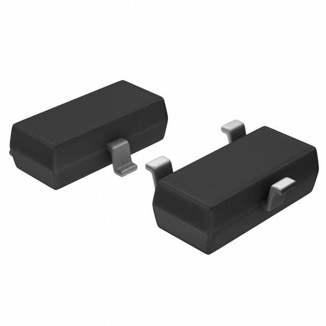
| 产品图片 |
|
| rohs | 符合RoHS无铅 / 符合限制有害物质指令(RoHS)规范要求 |
| 产品系列 | 电源管理 IC,监控电路,STMicroelectronics STM1810MWX7F- |
| NumberofInputsMonitored | 1 Input |
| 数据手册 | |
| 产品型号 | STM1810MWX7F |
| 产品培训模块 | http://www.digikey.cn/PTM/IndividualPTM.page?site=cn&lang=zhs&ptm=30015 |
| 产品目录页面 | |
| 产品种类 | 监控电路 |
| 人工复位 | No Manual Reset |
| 供应商器件封装 | SOT-23-3 |
| 其它名称 | 497-4960-1 |
| 其它有关文件 | http://www.st.com/web/catalog/sense_power/FM1946/SC665/PF94566?referrer=70071840 |
| 功率失效检测 | No |
| 包装 | 剪切带 (CT) |
| 受监控电压数 | 1 |
| 商标 | STMicroelectronics |
| 复位 | 低有效 |
| 复位超时 | 最小为 100 ms |
| 安装类型 | 表面贴装 |
| 安装风格 | SMD/SMT |
| 封装 | Reel |
| 封装/外壳 | TO-236-3,SC-59,SOT-23-3 |
| 封装/箱体 | SOT-23-3 |
| 工作温度 | -40°C ~ 105°C |
| 工作电源电流 | 16 uA |
| 工厂包装数量 | 3000 |
| 最大功率耗散 | 320 mW |
| 最大工作温度 | + 105 C |
| 最小工作温度 | - 40 C |
| 标准包装 | 1 |
| 欠电压阈值 | 4.25 V |
| 电压-阈值 | 4.37V |
| 电池备用开关 | No Backup |
| 电源电压-最大 | 5.5 V |
| 电源电压-最小 | 1.2 V |
| 监视器 | No Watchdog |
| 类型 | Voltage Supervisory |
| 系列 | STM1810 |
| 芯片启用信号 | No Chip Enable |
| 被监测输入数 | 1 Input |
| 输出 | 推挽式,图腾柱 |
| 输出类型 | Active Low, Push-Pull |
| 过电压阈值 | 4.49 V |
| 阈值电压 | 3 V, 3.3 V, 5 V |


- 商务部:美国ITC正式对集成电路等产品启动337调查
- 曝三星4nm工艺存在良率问题 高通将骁龙8 Gen1或转产台积电
- 太阳诱电将投资9.5亿元在常州建新厂生产MLCC 预计2023年完工
- 英特尔发布欧洲新工厂建设计划 深化IDM 2.0 战略
- 台积电先进制程称霸业界 有大客户加持明年业绩稳了
- 达到5530亿美元!SIA预计今年全球半导体销售额将创下新高
- 英特尔拟将自动驾驶子公司Mobileye上市 估值或超500亿美元
- 三星加码芯片和SET,合并消费电子和移动部门,撤换高东真等 CEO
- 三星电子宣布重大人事变动 还合并消费电子和移动部门
- 海关总署:前11个月进口集成电路产品价值2.52万亿元 增长14.8%


PDF Datasheet 数据手册内容提取
STM1810 STM1811 STM1812 STM1813 STM1815 STM1816 STM1817 STM1818 Low power reset circuit Features ■ Precision monitoring of 3 V, 3.3 V, and 5 V supply voltages ■ Four output configurations: – Push-pull, active-high (STM1812,1817) – Push-pull, active-low (STM1810,1815) – Open-drain, active-low (STM1811,1816) – Open-drain, active-low with push-button detect (STM1813,1818) ■ Reset pulse width - 100 ms (min.) SOT23-3 (WX) ■ Low supply current - 4 µA (typ.) ■ Guaranteed assertion down to V = 1.0 V CC (0 °C to 105 °C) ■ Factory-trimmed reset thresholds of 2.55 V, 2.88 V, 3.06 V, 4.37 V, and 4.62 V (typ.) ■ ± 2.5% reset threshold accuracy: (–40 °C to 105 °C) ■ Power supply transient immunity ■ Available in the SOT23-3 package ■ Push-button/manual reset detect (STM1813/1818) ■ Fully compatible with DS181x and MXD181x products. ■ Operating temperature: –40 °C to 105 °C Table 1. Device summary Active-low Active-low Active-high Active-low reset 3.3 V/ Order codes 5 V reset reset reset (open-drain, 3.0 V (push-pull) (open-drain) (push-pull) bidirectional, with MR detect) STM1810L/M ✔ ✔ STM1811L/M ✔ ✔(1) STM1812L/M ✔ ✔ STM1813L/M ✔ ✔ STM1815T/S/R ✔ ✔ STM1816T/S/R ✔ ✔(1) STM1817T/S/R ✔ ✔ STM1818T/S/R ✔ ✔ 1. Active-low RST with internal pull-up resistor. September 2010 Doc ID11464 Rev 8 1/25 www.st.com 1
Contents STM1810/1811/1812/1813/1815/1816/1817/1818 Contents 1 Description . . . . . . . . . . . . . . . . . . . . . . . . . . . . . . . . . . . . . . . . . . . . . . . . . 5 1.1 Functional block diagrams . . . . . . . . . . . . . . . . . . . . . . . . . . . . . . . . . . . . . 7 1.2 Pin descriptions . . . . . . . . . . . . . . . . . . . . . . . . . . . . . . . . . . . . . . . . . . . . . 7 1.2.1 Active-low RST output (push-pull) . . . . . . . . . . . . . . . . . . . . . . . . . . . . . . 7 1.2.2 Active-low RST output (open-drain) . . . . . . . . . . . . . . . . . . . . . . . . . . . . . 7 1.2.3 Active-high RST output (push-pull) . . . . . . . . . . . . . . . . . . . . . . . . . . . . . 8 1.2.4 Active-low RST output (open-drain with internal 5.5 kΩ pull-up) with manual reset detect . . . . . . . . . . . . . . . . . . . . . . . . . . . . . . . . . . . . . . . . . 8 1.2.5 V CC . . . . . . . . . . . . . . . . . . . . . . . . . . . . . . . . . . . . . . . . . . . . . . . . . . . . . . . . . . . . . . . . . . .8 1.2.6 V SS . . . . . . . . . . . . . . . . . . . . . . . . . . . . . . . . . . . . . . . . . . . . . . . . . . . . . . . . . . . . . . . . . . . .8 2 Operation . . . . . . . . . . . . . . . . . . . . . . . . . . . . . . . . . . . . . . . . . . . . . . . . . . 9 2.1 Reset output . . . . . . . . . . . . . . . . . . . . . . . . . . . . . . . . . . . . . . . . . . . . . . . . 9 2.2 Push-button detect reset (STM1813/1818) . . . . . . . . . . . . . . . . . . . . . . . . 9 2.3 Interfacing to bidirectional microcontrollers (MCU’s) . . . . . . . . . . . . . . . . . 9 2.4 Negative going V transients . . . . . . . . . . . . . . . . . . . . . . . . . . . . . . . . . . 9 CC 2.5 Valid RST output down to V = 0 V . . . . . . . . . . . . . . . . . . . . . . . . . . . . 10 CC 3 Typical operating characteristics . . . . . . . . . . . . . . . . . . . . . . . . . . . . . 13 4 Maximum rating . . . . . . . . . . . . . . . . . . . . . . . . . . . . . . . . . . . . . . . . . . . . 17 5 DC and AC parameters . . . . . . . . . . . . . . . . . . . . . . . . . . . . . . . . . . . . . . 18 6 Package mechanical . . . . . . . . . . . . . . . . . . . . . . . . . . . . . . . . . . . . . . . . 20 6.1 ECOPACK® . . . . . . . . . . . . . . . . . . . . . . . . . . . . . . . . . . . . . . . . . . . . . . . . . . . . . . . . . . . . 20 7 Part numbering . . . . . . . . . . . . . . . . . . . . . . . . . . . . . . . . . . . . . . . . . . . . 22 8 Revision history . . . . . . . . . . . . . . . . . . . . . . . . . . . . . . . . . . . . . . . . . . . 24 2/25 Doc ID11464 Rev 8
STM1810/1811/1812/1813/1815/1816/1817/1818 List of tables List of tables Table 1. Device summary. . . . . . . . . . . . . . . . . . . . . . . . . . . . . . . . . . . . . . . . . . . . . . . . . . . . . . . . . . 1 Table 2. Signal names . . . . . . . . . . . . . . . . . . . . . . . . . . . . . . . . . . . . . . . . . . . . . . . . . . . . . . . . . . . . 6 Table 3. STM1810/STM1815 . . . . . . . . . . . . . . . . . . . . . . . . . . . . . . . . . . . . . . . . . . . . . . . . . . . . . . . 8 Table 4. STM1811/STM1816 . . . . . . . . . . . . . . . . . . . . . . . . . . . . . . . . . . . . . . . . . . . . . . . . . . . . . . . 8 Table 5. STM1812/STM1817 . . . . . . . . . . . . . . . . . . . . . . . . . . . . . . . . . . . . . . . . . . . . . . . . . . . . . . . 8 Table 6. STM1813/STM1818 . . . . . . . . . . . . . . . . . . . . . . . . . . . . . . . . . . . . . . . . . . . . . . . . . . . . . . . 8 Table 7. Absolute maximum ratings. . . . . . . . . . . . . . . . . . . . . . . . . . . . . . . . . . . . . . . . . . . . . . . . . 17 Table 8. Operating and AC measurement conditions. . . . . . . . . . . . . . . . . . . . . . . . . . . . . . . . . . . . 18 Table 9. DC and AC characteristics . . . . . . . . . . . . . . . . . . . . . . . . . . . . . . . . . . . . . . . . . . . . . . . . . 19 Table 10. SOT23-3 – 3-lead small outline transistor package mechanical data. . . . . . . . . . . . . . . . . 21 Table 11. Ordering information scheme. . . . . . . . . . . . . . . . . . . . . . . . . . . . . . . . . . . . . . . . . . . . . . . 22 Table 12. Marking description. . . . . . . . . . . . . . . . . . . . . . . . . . . . . . . . . . . . . . . . . . . . . . . . . . . . . . . 23 Table 13. Document revision history . . . . . . . . . . . . . . . . . . . . . . . . . . . . . . . . . . . . . . . . . . . . . . . . . 24 Doc ID11464 Rev 8 3/25
List of figures STM1810/1811/1812/1813/1815/1816/1817/1818 List of figures Figure 1. Logic diagram. . . . . . . . . . . . . . . . . . . . . . . . . . . . . . . . . . . . . . . . . . . . . . . . . . . . . . . . . . . . 5 Figure 2. SOT23-3 connections. . . . . . . . . . . . . . . . . . . . . . . . . . . . . . . . . . . . . . . . . . . . . . . . . . . . . . 6 Figure 3. Hardware hookup. . . . . . . . . . . . . . . . . . . . . . . . . . . . . . . . . . . . . . . . . . . . . . . . . . . . . . . . . 6 Figure 4. Push-pull active-low output (STM1810/1812/1815/1817). . . . . . . . . . . . . . . . . . . . . . . . . . . 7 Figure 5. Open-drain, active-low output (STM1811/1816). . . . . . . . . . . . . . . . . . . . . . . . . . . . . . . . . . 7 Figure 6. Open-drain, active-low output (bidirectional, manual reset detect, STM1813/1818) . . . . . . 7 Figure 7. Reset timing diagram . . . . . . . . . . . . . . . . . . . . . . . . . . . . . . . . . . . . . . . . . . . . . . . . . . . . . 10 Figure 8. Push-button manual reset with MR detect (STM1813/1818) . . . . . . . . . . . . . . . . . . . . . . . 10 Figure 9. Manual reset timing diagram, switch bounce/debounce (STM1813/1818). . . . . . . . . . . . . 11 Figure 10. Interfacing MCUs with bidirectional reset pins (RST, open-drain, STM1811/1816) . . . . . . 11 Figure 11. Valid reset (RST) output down to V = 0 V (push-pull). . . . . . . . . . . . . . . . . . . . . . . . . . . 11 CC Figure 12. Valid reset (RST) output down to V = 0 V (push-pull). . . . . . . . . . . . . . . . . . . . . . . . . . . 12 CC Figure 13. Supply current vs. temperature (no load). . . . . . . . . . . . . . . . . . . . . . . . . . . . . . . . . . . . . . 13 Figure 14. Normalized reset time-out period (t ) vs. temperature - V = V – V . . . . . . . . . . . 13 rec OD TH CC Figure 15. V -to-reset output delay vs. temperature - V = V – V . . . . . . . . . . . . . . . . . . . . . 14 CC OD TH CC Figure 16. Voltage output low vs. I SINK . . . . . . . . . . . . . . . . . . . . . . . . . . . . . . . . . . . . . . . . . . . . . . . . . . . . . . . . . . . . .14 Figure 17. Voltage output high vs. I SOURCE. . . . . . . . . . . . . . . . . . . . . . . . . . . . . . . . . . . . . . . . . . . . . . . . . . . . . . . . .15 Figure 18. Normalized reset threshold vs. temperature. . . . . . . . . . . . . . . . . . . . . . . . . . . . . . . . . . . . 15 Figure 19. Max. transient duration NOT causing reset pulse vs. reset threshold overdrive. . . . . . . . . 16 Figure 20. AC testing input/output waveforms. . . . . . . . . . . . . . . . . . . . . . . . . . . . . . . . . . . . . . . . . . . 18 Figure 21. SOT23-3 – 3-lead small outline transistor package outline . . . . . . . . . . . . . . . . . . . . . . . . 20 4/25 Doc ID11464 Rev 8
STM1810/1811/1812/1813/1815/1816/1817/1818 Description 1 Description STM181x devices are low power reset devices used to monitor power supplies for microcontrollers. They perform a single function: asserting a reset signal whenever V CC supply voltage drops below a preset value and keeping it asserted until V has risen above CC the preset threshold for a minimum period of time (t ). They provide excellent circuit rec reliability without additional external components when used with +3.0 V / +3.3 V (STM1815–STM1818), and +5 V (STM1810–STM1813) power supply systems. A precision voltage reference and comparator monitors the V input for an out-of-tolerance CC condition. When an invalid V condition occurs, the reset output (RST) is forced low CC (or high in the case of RST) and remains asserted for t after V rises above the reset rec CC threshold. The STM1813/1818 also keep reset asserted for t after the output is rec momentarily pulled to ground by an external push-button switch. The STM1812 and STM1817 have an active-high, push-pull output. The STM1810 and STM1815 (push-pull) and STM1811, STM1813, STM1816, and STM1818 (open-drain) have an active-low RST output. The open-drain devices (STM1811 / STM1813 / STM1816 / STM1818) also have an internal pull-up resistor to V . The STM1813 and STM1818 CC feature a debounced manual reset feature that asserts a reset if the RST pin is pulled low for more than 1.5 µs. When used to initiate manual reset, RST debounces signals from devices such as mechanical switches. For devices with this feature, the release of the external switch triggers the reset period. The STM181x devices are guaranteed to output the correct logic state for V down to CC 1.0 V (0 °C to +105 °C). They also provide a reset comparator designed to ignore fast transients on V . CC Reset thresholds are available between +2.55 V and +4.62 V. These small, low power devices are ideal for use in portable equipment. All are available in the space-saving 3-pin SOT23 package, and are specified from –40 °C to +105 °C. Figure 1. Logic diagram (cid:54) (cid:35)(cid:35) (cid:51)(cid:52)(cid:45)(cid:17)(cid:24)(cid:17)(cid:88) (cid:50)(cid:51)(cid:52)(cid:0)(cid:8)(cid:50)(cid:51)(cid:52)(cid:9)(cid:8)(cid:17)(cid:9) (cid:54) (cid:51)(cid:51) (cid:33)(cid:41)(cid:16)(cid:25)(cid:22)(cid:20)(cid:24) 1. For STM1812, STM1817. Doc ID11464 Rev 8 5/25
Description STM1810/1811/1812/1813/1815/1816/1817/1818 T able 2. Signal names Symbol Description V Ground SS RST Active-low reset output RST(1) Active-high reset output V Supply voltage and input for reset threshold monitor CC 1. For STM1812, STM1817. Figure 2. SOT23-3 connections (cid:50)(cid:51)(cid:52)(cid:0)(cid:8)(cid:50)(cid:51)(cid:52)(cid:9) (cid:17) (cid:19) (cid:54)(cid:51)(cid:51) (cid:54)(cid:35)(cid:35) (cid:18) (cid:33)(cid:41)(cid:16)(cid:25)(cid:22)(cid:20)(cid:25) 2. RST for STM1812 and STM1817. Figure 3. Hardware hookup (cid:54) (cid:35)(cid:35) (cid:54)(cid:35)(cid:35) (cid:54)(cid:35)(cid:35) (cid:51)(cid:52)(cid:45)(cid:17)(cid:24)(cid:17)(cid:88) (cid:45)(cid:35)(cid:53) (cid:50)(cid:69)(cid:83)(cid:69)(cid:84) (cid:50)(cid:51)(cid:52)(cid:8)(cid:17)(cid:9) (cid:41)(cid:78)(cid:80)(cid:85)(cid:84) (cid:48)(cid:85)(cid:83)(cid:72)(cid:13)(cid:66)(cid:85)(cid:84)(cid:84)(cid:79)(cid:78) (cid:8)(cid:18)(cid:9) (cid:54)(cid:51)(cid:51) (cid:82)(cid:69)(cid:83)(cid:69)(cid:84) (cid:54)(cid:51)(cid:51) (cid:33)(cid:41)(cid:16)(cid:25)(cid:22)(cid:21)(cid:18)(cid:65) 1. RST for STM1812 and STM1817 (see Table1). 2. Only valid for STM1813 and STM1818. 6/25 Doc ID11464 Rev 8
STM1810/1811/1812/1813/1815/1816/1817/1818 Description 1.1 Functional block diagrams Figure 4. Push-pull active-low output (STM1810/1812/1815/1817) (cid:54)(cid:35)(cid:35) (cid:54)(cid:50)(cid:51)(cid:52) (cid:35)(cid:47)(cid:45)(cid:48)(cid:33)(cid:50)(cid:37) (cid:71)(cid:69)(cid:78)(cid:84)(cid:82)(cid:69)(cid:69)(cid:82)(cid:67)(cid:65)(cid:84)(cid:79)(cid:82) (cid:50)(cid:51)(cid:52)(cid:8)(cid:17)(cid:9) (cid:33)(cid:41)(cid:16)(cid:25)(cid:22)(cid:21)(cid:17)(cid:65) 1. RST for STM1812 and STM1817. Figure 5. Open-drain, active-low output (STM1811/1816) (cid:54)(cid:35)(cid:35) (cid:84)(cid:82)(cid:69)(cid:67) (cid:54)(cid:50)(cid:51)(cid:52) (cid:35)(cid:47)(cid:45)(cid:48)(cid:33)(cid:50)(cid:37) (cid:71)(cid:69)(cid:78)(cid:69)(cid:82)(cid:65)(cid:84)(cid:79)(cid:82) (cid:50)(cid:51)(cid:52) (cid:33)(cid:41)(cid:16)(cid:25)(cid:22)(cid:23)(cid:18) 1. 5.5 kΩ internal pull-up resistor. Figure 6. Open-drain, active-low output (bidirectional, manual reset detect, STM1813/1818) (cid:48)(cid:85)(cid:83)(cid:72)(cid:13)(cid:66)(cid:85)(cid:84)(cid:84)(cid:79)(cid:78) (cid:68)(cid:69)(cid:84)(cid:69)(cid:67)(cid:84) (cid:50)(cid:51)(cid:52) (cid:54)(cid:35)(cid:35) (cid:84)(cid:82)(cid:69)(cid:67) (cid:54)(cid:50)(cid:51)(cid:52) (cid:35)(cid:47)(cid:45)(cid:48)(cid:33)(cid:50)(cid:37) (cid:71)(cid:69)(cid:78)(cid:69)(cid:82)(cid:65)(cid:84)(cid:79)(cid:82) (cid:33)(cid:41)(cid:16)(cid:25)(cid:22)(cid:23)(cid:19) 1. 5.5 kΩ internal pull-up resistor. 1.2 Pin descriptions See Figure1 and Table2 for a brief overview of the signals connected to this device. 1.2.1 Active-low RST output (push-pull) Pulses low when V drops below V , and stays low as long as V is below the reset CC RST CC threshold. It remains low for t after V rises above the reset threshold. rec CC 1.2.2 Active-low RST output (open-drain) Pulses low when V drops below V , and stays low as long as V is below the reset CC RST CC threshold. It remains low for t after V rises above the reset threshold. RST output has rec CC an internal 5.5 kΩ pull-up resistor. Doc ID11464 Rev 8 7/25
Description STM1810/1811/1812/1813/1815/1816/1817/1818 1.2.3 Active-high RST output (push-pull) Pulses high when V drops below V , and stays high as long as V is below the reset CC RST CC threshold. It remains high for t after V rises above the reset threshold. rec CC 1.2.4 Active-low RST output (open-drain with internal 5.5 kΩ pull-up) with manual reset detect Pulses low when V drops below V , or RST is externally pulled low for at least 1.5 µs. CC RST It remains low for t after V rises above the reset threshold, or after the external PBRST CC manual reset is released (see Figure9). RST output has an internal 5.5 kΩ pull-up resistor. 1.2.5 V CC Supply voltage and input for V comparator. RST 1.2.6 V SS Ground, is the reference for the power supply. It must be connected to the system ground. T able 3. STM1810/STM1815 Pin Name Function 1 RST Active-low reset output (push-pull) 2 V Supply voltage and input for reset threshold monitor CC 3 V Ground SS T able 4. STM1811/STM1816 Pin Name Function 1 RST Active-low reset output (open-drain, with internal 5.5 kΩ pull-up resistor) 2 V Supply voltage and input for reset threshold monitor CC 3 V Ground SS T able 5. STM1812/STM1817 Pin Name Function 1 RST Active-high reset output (push-pull) 2 V Supply voltage and input for reset threshold monitor CC 3 V Ground SS T able 6. STM1813/STM1818 Pin Name Function 1 RST Active-low reset output (open-drain, with internal 5.5 kΩ pull-up) with push- button/manual reset detect 2 V Supply voltage and input for reset threshold monitor CC 3 V Ground SS 8/25 Doc ID11464 Rev 8
STM1810/1811/1812/1813/1815/1816/1817/1818 Operation 2 Operation 2.1 Reset output The STM181x asserts a reset signal to the microcontroller (MCU) whenever V goes CC below the reset threshold (V ), and is guaranteed valid down to V = 1.0 V (0 °C to RST CC 105 °C). A microcontroller’s (MCU) reset input starts the MCU in a known state. The STM1810 - STM1813/ STM1815 - STM1818 low power reset circuits assert reset to prevent code-execution errors during power-up, power-down, and brownout conditions (Figure7). During power-up, once V exceeds the reset threshold an internal timer keeps RST low for CC the reset time-out period, t . After this interval, RST returns high. rec If V drops below the reset threshold, RST goes low. Each time RST is asserted, it stays CC low for at least the reset time-out period. Any time V goes below the reset threshold, the CC internal timer clears. The reset timer starts when V returns above the reset threshold. CC Reset t is also triggered by an externally initiated rising edge on the RST pin rec (STM1813/STM1818), following a low signal of 1.5 µs minimum duration. 2.2 Push-button detect reset (STM1813/1818) Many systems require push-button reset capability (Figure8), allowing the user or external logic circuitry to initiate reset. On the STM1813/STM1818, a logic low on RST held for greater than 1.5 µs asserts a reset. RST deasserts following a 100 ms minimum reset time- out delay (t ). A manual reset input shorter than 1.5 µs may release RST without the rec 100 ms minimum reset time-out delay. To facilitate use with mechanical switches, the STM1813/STM1818 contain internal debounce circuitry. A debounced waveform is shown in Figure9 The RST output has an internal 5.5 kΩ pull-up resistor. 2.3 Interfacing to bidirectional microcontrollers (MCU’s) As the RST output on the STM1811/STM1816 is open-drain, these devices interface easily with MCU’s that have bidirectional reset pins. Connecting the µP supervisor’s reset (RST) output directly to the microcontroller’s reset (RST) pin allows either device to assert reset (Figure10). No external pull-up resistor is required, as it is within the STM1811/STM1816. 2.4 Negative going V transients CC The STM181x are relatively immune to negative-going V transients (glitches). Figure19 CC shows typical transient duration versus reset comparator overdrive (for which the STM181x will NOT generate a reset pulse). The graph was generated using a negative pulse applied to V starting at 0.5 V above the actual reset threshold and ending below it by the CC, magnitude indicated (comparator overdrive). The graph indicates the maximum pulse width a negative V transient can have without causing a reset pulse. As the magnitude of the CC transient increases (further below the threshold), the maximum allowable pulse width decreases. Any combination of duration and overdrive which lies under the curve will NOT generate a reset signal. Typically, a V transient that goes 100 mV below the reset CC threshold and lasts 20 µs or less will not cause a reset pulse. A 0.1 µF bypass capacitor mounted as close as possible to the V pin provides additional transient immunity. CC Doc ID11464 Rev 8 9/25
Operation STM1810/1811/1812/1813/1815/1816/1817/1818 2.5 Valid RST output down to V = 0 V CC When V falls below 1 V, the RST output no longer sinks current, but becomes an open CC circuit. In most systems this is not a problem, as most MCUs do not operate below 1 V. However, in applications where RST output must be valid down to 0 V, a pull-down resistor may be added to hold the RST output low (see Figure11). This resistor must be large enough to not load the RST output, and still be small enough to pull the output to ground. A 100 kΩ resistor is recommended. Note: The same situation applies for the active-high RST of the STM1810/1812. A 100 kΩ pull-up resistor to V should be used if RST must remain valid for V < 1.0 V. CC CC Figure 7. Reset timing diagram (cid:54)(cid:35)(cid:35) (cid:54)(cid:50)(cid:51)(cid:52) (cid:50)(cid:51)(cid:52) (cid:54)(cid:35)(cid:35)(cid:0)(cid:8)(cid:77)(cid:73)(cid:78)(cid:9) (cid:84)(cid:82)(cid:69)(cid:67) (cid:84)(cid:82)(cid:69)(cid:67) (cid:8)(cid:17)(cid:9) (cid:50)(cid:51)(cid:52) (cid:33)(cid:41)(cid:16)(cid:25)(cid:22)(cid:21)(cid:19) 1. RST for STM1812 and STM1817. Figure 8. Push-button manual reset with MR detect (STM1813/1818) (cid:54) (cid:35)(cid:35) (cid:51)(cid:52)(cid:45)(cid:17)(cid:24)(cid:17)(cid:19) (cid:54)(cid:35)(cid:35) (cid:51)(cid:52)(cid:45)(cid:17)(cid:24)(cid:17)(cid:24) (cid:50)(cid:69)(cid:83)(cid:69)(cid:84) (cid:45)(cid:73)(cid:67)(cid:82)(cid:79)(cid:0)(cid:50)(cid:37)(cid:51)(cid:37)(cid:52) (cid:77)(cid:79)(cid:78)(cid:73)(cid:84)(cid:79)(cid:82) (cid:50)(cid:51)(cid:52) (cid:48)(cid:85)(cid:83)(cid:72)(cid:13)(cid:66)(cid:85)(cid:84)(cid:84)(cid:79)(cid:78)(cid:0)(cid:50)(cid:37)(cid:51)(cid:37)(cid:52) (cid:54)(cid:51)(cid:51) (cid:33)(cid:41)(cid:16)(cid:25)(cid:22)(cid:21)(cid:20) 10/25 Doc ID11464 Rev 8
STM1810/1811/1812/1813/1815/1816/1817/1818 Operation Figure 9. Manual reset timing diagram, switch bounce/debounce (STM1813/1818) (cid:54)(cid:35)(cid:35) (cid:84)(cid:48)(cid:34)(cid:50)(cid:51)(cid:52) (cid:84)(cid:48)(cid:34)(cid:50)(cid:51)(cid:52) (cid:8)(cid:47)(cid:80)(cid:69)(cid:78)(cid:9) (cid:51)(cid:87)(cid:73)(cid:84)(cid:67)(cid:72)(cid:0)(cid:66)(cid:79)(cid:85)(cid:78)(cid:67)(cid:69) (cid:37)(cid:88)(cid:84)(cid:69)(cid:82)(cid:78)(cid:65)(cid:76) (cid:8)(cid:35)(cid:76)(cid:79)(cid:83)(cid:69)(cid:68)(cid:9) (cid:80)(cid:85)(cid:83)(cid:72)(cid:13)(cid:66)(cid:85)(cid:84)(cid:84)(cid:79)(cid:78) (cid:50)(cid:51)(cid:52) (cid:33)(cid:41)(cid:16)(cid:25)(cid:22)(cid:21)(cid:21) Figure 10. Interfacing MCUs with bidirectional reset pins (RST, open-drain, STM1811/1816) (cid:54) (cid:35)(cid:35) (cid:51)(cid:52)(cid:45)(cid:17)(cid:24)(cid:17)(cid:17) (cid:54)(cid:35)(cid:35) (cid:54)(cid:35)(cid:35) (cid:51)(cid:52)(cid:45)(cid:17)(cid:24)(cid:17)(cid:22) (cid:45)(cid:35)(cid:53) (cid:50)(cid:51)(cid:52) (cid:50)(cid:51)(cid:52) (cid:73)(cid:78)(cid:80)(cid:85)(cid:84) (cid:54)(cid:51)(cid:51) (cid:54)(cid:51)(cid:51) (cid:33)(cid:41)(cid:16)(cid:25)(cid:22)(cid:21)(cid:22) Figure 11. Valid reset (RST) output down to V = 0 V (push-pull) CC (cid:54) (cid:35)(cid:35) (cid:51)(cid:52)(cid:45)(cid:17)(cid:24)(cid:17)(cid:16) (cid:54) (cid:54) (cid:35)(cid:35) (cid:35)(cid:35) (cid:51)(cid:52)(cid:45)(cid:17)(cid:24)(cid:17)(cid:21) (cid:45)(cid:35)(cid:53) (cid:50)(cid:51)(cid:52) (cid:50)(cid:51)(cid:52) (cid:73)(cid:78)(cid:80)(cid:85)(cid:84) (cid:54)(cid:51)(cid:51) (cid:50)(cid:48)(cid:8)(cid:17)(cid:9) (cid:54)(cid:51)(cid:51) (cid:33)(cid:41)(cid:16)(cid:25)(cid:22)(cid:21)(cid:23) 1. ~100 kΩ resistor recommended. Doc ID11464 Rev 8 11/25
Operation STM1810/1811/1812/1813/1815/1816/1817/1818 Figure 12. Valid reset (RST) output down to V = 0 V (push-pull) CC (cid:54) (cid:35)(cid:35) (cid:51)(cid:52)(cid:45)(cid:17)(cid:24)(cid:17)(cid:18) (cid:54)(cid:35)(cid:35) (cid:54)(cid:35)(cid:35) (cid:51)(cid:52)(cid:45)(cid:17)(cid:24)(cid:17)(cid:23) (cid:50)(cid:48)(cid:8)(cid:17)(cid:9) (cid:45)(cid:35)(cid:53) (cid:50)(cid:51)(cid:52) (cid:50)(cid:51)(cid:52) (cid:41)(cid:78)(cid:80)(cid:85)(cid:84) (cid:54)(cid:51)(cid:51) (cid:54)(cid:51)(cid:51) (cid:33)(cid:41)(cid:16)(cid:25)(cid:22)(cid:21)(cid:24) 1. ~100 kΩ resistor recommended. 12/25 Doc ID11464 Rev 8
STM1810/1811/1812/1813/1815/1816/1817/1818 Typical operating characteristics 3 Typical operating characteristics Typical values are at T = 25 °C. A Figure 13. Supply current vs. temperature (no load) (cid:17)(cid:16) (cid:24) (cid:9) (cid:33) (cid:151) (cid:8) (cid:78)(cid:84)(cid:0) (cid:22) (cid:69) (cid:82) (cid:82) (cid:85) (cid:67) (cid:89)(cid:0) (cid:80)(cid:76) (cid:20) (cid:80) (cid:51)(cid:85) (cid:54)(cid:35)(cid:35)(cid:0)(cid:29)(cid:0)(cid:19)(cid:0)(cid:54) (cid:54)(cid:35)(cid:35)(cid:0)(cid:29)(cid:0)(cid:21)(cid:0)(cid:54) (cid:18) (cid:16) (cid:110)(cid:20)(cid:16) (cid:110)(cid:18)(cid:16) (cid:16) (cid:18)(cid:16) (cid:20)(cid:16) (cid:22)(cid:16) (cid:24)(cid:16) (cid:17)(cid:16)(cid:16) (cid:52)(cid:69)(cid:77)(cid:80)(cid:69)(cid:82)(cid:65)(cid:84)(cid:85)(cid:82)(cid:69)(cid:0)(cid:8)(cid:160)(cid:35)(cid:9) (cid:33)(cid:41)(cid:17)(cid:16)(cid:20)(cid:16)(cid:18)(cid:66) Figure 14. Normalized reset time-out period (t ) vs. temperature rec - V = V – V OD TH CC (cid:17)(cid:21)(cid:21) (cid:17)(cid:21)(cid:19) (cid:9)(cid:0) (cid:83) (cid:77) (cid:8) (cid:17)(cid:21)(cid:17) (cid:68)(cid:0) (cid:79) (cid:69)(cid:82)(cid:73) (cid:17)(cid:20)(cid:25) (cid:80) (cid:85)(cid:84)(cid:0) (cid:17)(cid:20)(cid:23) (cid:79) (cid:13) (cid:69) (cid:77) (cid:17)(cid:20)(cid:21) (cid:69)(cid:84)(cid:0)(cid:84)(cid:73) (cid:83) (cid:17)(cid:20)(cid:19) (cid:69) (cid:82) (cid:68)(cid:0) (cid:69) (cid:17)(cid:20)(cid:17) (cid:90) (cid:65)(cid:76)(cid:73) (cid:77) (cid:17)(cid:19)(cid:25) (cid:82) (cid:79) (cid:46) (cid:17)(cid:19)(cid:23) (cid:17)(cid:19)(cid:21) (cid:110)(cid:20)(cid:16) (cid:110)(cid:18)(cid:16) (cid:16) (cid:18)(cid:16) (cid:20)(cid:16) (cid:22)(cid:16) (cid:24)(cid:16) (cid:17)(cid:16)(cid:16) (cid:52)(cid:69)(cid:77)(cid:80)(cid:69)(cid:82)(cid:65)(cid:84)(cid:85)(cid:82)(cid:69)(cid:0)(cid:8)(cid:160)(cid:35)(cid:9) (cid:33)(cid:41)(cid:17)(cid:16)(cid:20)(cid:16)(cid:19)(cid:66) Doc ID11464 Rev 8 13/25
Typical operating characteristics STM1810/1811/1812/1813/1815/1816/1817/1818 Figure 15. V -to-reset output delay vs. temperature - V = V – V CC OD TH CC (cid:21) (cid:20) (cid:19) (cid:18) (cid:17) (cid:16) (cid:110)(cid:20)(cid:16) (cid:110)(cid:18)(cid:16) (cid:16) (cid:18)(cid:16) (cid:20)(cid:16) (cid:22)(cid:16) (cid:24)(cid:16) (cid:17)(cid:16)(cid:16) (cid:52)(cid:69)(cid:77)(cid:80)(cid:69)(cid:82)(cid:65)(cid:84)(cid:85)(cid:82)(cid:69)(cid:0)(cid:8)(cid:160)(cid:35)(cid:9) (cid:33)(cid:41)(cid:17)(cid:16)(cid:20)(cid:16)(cid:20)(cid:66) Figure 16. Voltage output low vs. I SINK (cid:16)(cid:14)(cid:18)(cid:16) (cid:16)(cid:14)(cid:17)(cid:22) (cid:9) (cid:54) (cid:8) (cid:69)(cid:0) (cid:65)(cid:71) (cid:16)(cid:14)(cid:17)(cid:18) (cid:79)(cid:76)(cid:84) (cid:86) (cid:85)(cid:84)(cid:0) (cid:80) (cid:16)(cid:14)(cid:16)(cid:24) (cid:85)(cid:84) (cid:47) (cid:16)(cid:14)(cid:16)(cid:20) (cid:16)(cid:14)(cid:16)(cid:16) (cid:16) (cid:19) (cid:22) (cid:25) (cid:17)(cid:18) (cid:47)(cid:85)(cid:84)(cid:80)(cid:85)(cid:84)(cid:0)(cid:67)(cid:85)(cid:82)(cid:82)(cid:69)(cid:78)(cid:84)(cid:0)(cid:8)(cid:77)(cid:33)(cid:9) (cid:33)(cid:41)(cid:17)(cid:16)(cid:20)(cid:16)(cid:22)(cid:66) 14/25 Doc ID11464 Rev 8
STM1810/1811/1812/1813/1815/1816/1817/1818 Typical operating characteristics Figure 17. Voltage output high vs. I SOURCE (cid:16)(cid:14)(cid:19)(cid:16) (cid:16)(cid:14)(cid:18)(cid:21) (cid:9) (cid:54) (cid:0)(cid:8)(cid:52) (cid:16)(cid:14)(cid:18)(cid:16) (cid:53) (cid:47) (cid:54) (cid:16)(cid:14)(cid:17)(cid:21) (cid:13)(cid:0) (cid:0)(cid:35) (cid:35) (cid:16)(cid:14)(cid:17)(cid:16) (cid:54) (cid:54)(cid:35)(cid:35)(cid:0)(cid:29)(cid:0)(cid:19)(cid:0)(cid:54) (cid:16)(cid:14)(cid:16)(cid:21) (cid:16)(cid:14)(cid:16)(cid:16) (cid:16)(cid:14)(cid:16) (cid:16)(cid:14)(cid:21) (cid:17)(cid:14)(cid:16) (cid:17)(cid:14)(cid:21) (cid:18)(cid:14)(cid:16) (cid:18)(cid:14)(cid:21) (cid:19)(cid:14)(cid:16) (cid:47)(cid:85)(cid:84)(cid:80)(cid:85)(cid:84)(cid:0)(cid:67)(cid:85)(cid:82)(cid:82)(cid:69)(cid:78)(cid:84)(cid:0)(cid:8)(cid:77)(cid:33)(cid:9) (cid:33)(cid:41)(cid:17)(cid:16)(cid:20)(cid:16)(cid:23)(cid:66) Figure 18. Normalized reset threshold vs. temperature (cid:17)(cid:14)(cid:16)(cid:17)(cid:16) (cid:68) (cid:79)(cid:76) (cid:17)(cid:14)(cid:16)(cid:16)(cid:21) (cid:72) (cid:83) (cid:69) (cid:82) (cid:72) (cid:69)(cid:84)(cid:0)(cid:84) (cid:83) (cid:69) (cid:17)(cid:14)(cid:16)(cid:16)(cid:16) (cid:82) (cid:68)(cid:0) (cid:69) (cid:90) (cid:65)(cid:76)(cid:73) (cid:77) (cid:82) (cid:79) (cid:16)(cid:14)(cid:25)(cid:25)(cid:21) (cid:46) (cid:16)(cid:14)(cid:25)(cid:25)(cid:16) (cid:110)(cid:20)(cid:16) (cid:110)(cid:18)(cid:16) (cid:16) (cid:18)(cid:16) (cid:20)(cid:16) (cid:22)(cid:16) (cid:24)(cid:16) (cid:17)(cid:16)(cid:16) (cid:52)(cid:69)(cid:77)(cid:80)(cid:69)(cid:82)(cid:65)(cid:84)(cid:85)(cid:82)(cid:69)(cid:0)(cid:8)(cid:160)(cid:35)(cid:9) (cid:33)(cid:41)(cid:17)(cid:16)(cid:20)(cid:16)(cid:21)(cid:66) Doc ID11464 Rev 8 15/25
Typical operating characteristics STM1810/1811/1812/1813/1815/1816/1817/1818 Figure 19. Max. transient duration NOT causing reset pulse vs. reset threshold overdrive (cid:21)(cid:16) (cid:20)(cid:21) (cid:20)(cid:16) (cid:19)(cid:21) (cid:19)(cid:16) (cid:18)(cid:21) (cid:18)(cid:16) (cid:17)(cid:21) (cid:17)(cid:16) (cid:21) (cid:16) (cid:17)(cid:16) (cid:17)(cid:16)(cid:16) (cid:17)(cid:16)(cid:16)(cid:16) (cid:50)(cid:69)(cid:83)(cid:69)(cid:84)(cid:0)(cid:84)(cid:72)(cid:82)(cid:69)(cid:83)(cid:72)(cid:79)(cid:76)(cid:68)(cid:0)(cid:79)(cid:86)(cid:69)(cid:82)(cid:68)(cid:82)(cid:73)(cid:86)(cid:69)(cid:0)(cid:8)(cid:77)(cid:54)(cid:9) (cid:33)(cid:41)(cid:17)(cid:16)(cid:20)(cid:16)(cid:24)(cid:66) 1. Reset occurs above the line. 16/25 Doc ID11464 Rev 8
STM1810/1811/1812/1813/1815/1816/1817/1818 Maximum rating 4 Maximum rating Stressing the device above the rating listed in Table7 may cause permanent damage to the device. These are stress ratings only and operation of the device at these or any other conditions above those indicated in the “Operating” sections of this specification is not implied. Exposure to absolute maximum rating conditions for extended periods may affect device reliability. Refer also to the STMicroelectronics™ “SURE Program” and other relevant quality documents. T able 7. Absolute maximum ratings Symbol Parameter Value Unit T Storage temperature (V Off) –55 to 150 °C STG CC T (1) Lead solder temperature for 10 seconds 260 °C SLD V Input or output voltage –0.3 to V +0.3 V IO CC V Supply voltage –0.3 to 7.0 V CC I Output current 20 mA O P Power dissipation 320 mW D 1. Reflow at peak temperature of 255 °C to 260 °C for < 30 seconds (total thermal budget not to exceed 180 °C for between 90 to 150 seconds). Doc ID11464 Rev 8 17/25
DC and AC parameters STM1810/1811/1812/1813/1815/1816/1817/1818 5 DC and AC parameters This section summarizes the operating measurement conditions, and the DC and AC characteristics of the device. The parameters in the DC and AC characteristics tables that follow, are derived from tests performed under the measurement conditions summarized in Table8. Designers should check that the operating conditions in their circuit match the operating conditions when relying on the quoted parameters. T able 8. Operating and AC measurement conditions Parameter STM1810 - 1818 Unit V supply voltage 1.0 to 5.5 V CC Ambient operating temperature (T ) –40 to 105 °C A Input rise and fall times ≤ 5 ns Input pulse voltages 0.2 to 0.8 V V CC Input and output timing ref. voltages 0.3 to 0.7 V V CC Figure 20. AC testing input/output waveforms (cid:16)(cid:14)(cid:24)(cid:0)(cid:54)(cid:35)(cid:35) (cid:16)(cid:14)(cid:23)(cid:0)(cid:54)(cid:35)(cid:35) (cid:16)(cid:14)(cid:19)(cid:0)(cid:54) (cid:35)(cid:35) (cid:16)(cid:14)(cid:18)(cid:0)(cid:54)(cid:35)(cid:35) (cid:33)(cid:41)(cid:16)(cid:18)(cid:21)(cid:22)(cid:24) 18/25 Doc ID11464 Rev 8
STM1810/1811/1812/1813/1815/1816/1817/1818 DC and AC parameters Table 9. D C and AC characteristics Alter- Sym. Description Test condition(1) Min. Typ. Max. Unit native T = 0 to +105 °C 1.0 5.5 V A V Operating voltage CC T = –40 to +105 °C 1.2 5.5 V A V = 3.6 V, no load 4 10 µA CC I V supply current CC CC V = 5.5 V, no load 9 16 µA CC 0.7 V Input high voltage STM1813/1818 only V IH V CC V Input low voltage STM1813/1818 only 0.4 V IL V V V Output high voltage 0 < I < 500 µA CC CC V OH OH – 0.5 – 0.1 V ≥ V (max.), reset not asserted RST output source current CC RST 350 µA (STM1810/STM1815) I OH V ≤ V (min.), reset asserted RST output source current CC RST 350 µA (STM1812/STM1817) V ≥ 2.7 V, reset asserted, CC RST output sink current V = 0.4 V 10 mA OUT I (STM1810/1811/1813/1815/1816/1818) OL V ≥ 2.7 V, reset not asserted, RST output sink current CC 10 mA V = 0.4 V, (STM1812/1817) OUT C Output capacitance(2) 10 pF OUT Reset thresholds 25 °C 4.62 V STM181xL –40 to 105 °C 4.50 4.75 V 25 °C 4.37 V STM181xM –40 to 105 °C 4.25 4.49 V 25 °C 3.06 V V Reset threshold STM181xT RST –40 to 105 °C 2.98 3.15 V 25 °C 2.88 V STM181xS –40 to 105 °C 2.80 2.97 V 25 °C 2.55 V STM181xR –40 to 105 °C 2.47 2.64 V V = (V + 100 mV) falling to t V to RST delay CC TH 2 5 µs RD CC (V – 200 mV) TH t RST pulse width V Rising 100 150 200 ms rec CC Push-button reset detect (STM1813, STM1818) t Push-button detect to RST STM1813/1818 1.5 µs PB t Push-button RST time-out From rising edge 100 150 200 ms PBRST STM1811/1816 3.5 5.5 7.5 kΩ Internal pull-up resistance STM1813/1818 3.1 5.5 7.5 kΩ 1. Valid for ambient operating temperature: T = –40 °C to 105 °C; V = 1.2 V to 5.5 V (except where noted). A CC 2. The STM1811/1813/1816/1818 have an internal pull-up resistor which may sink 1 mA of current. Doc ID11464 Rev 8 19/25
Package mechanical STM1810/1811/1812/1813/1815/1816/1817/1818 6 Package mechanical ® 6.1 ECOPACK In order to meet environmental requirements, ST offers these devices in different grades of ECOPACK® packages, depending on their level of environmental compliance. ECOPACK® specifications, grade definitions and product status are available at: www.st.com. ECOPACK® is an ST trademark. Figure 21. SOT23-3 – 3-lead small outline transistor package outline (cid:37) (cid:37)(cid:17) (cid:34) (cid:16)(cid:14)(cid:17)(cid:21) (cid:45) (cid:35) (cid:33) (cid:34) (cid:33)(cid:17) (cid:17) (cid:69) (cid:69)(cid:17) (cid:36) (cid:19)(cid:56) (cid:16)(cid:14)(cid:18)(cid:16) (cid:45) (cid:35) (cid:33) (cid:34) (cid:16)(cid:14)(cid:17)(cid:16) (cid:35) (cid:33)(cid:18) (cid:33) (cid:19)(cid:56)(cid:0)(cid:66) (cid:35) (cid:33) (cid:35) (cid:44)(cid:17) (cid:35) (cid:44) (cid:51)(cid:47)(cid:52)(cid:18)(cid:19)(cid:13)(cid:19) 1. Drawing is not to scale. 20/25 Doc ID11464 Rev 8
STM1810/1811/1812/1813/1815/1816/1817/1818 Package mechanical T able 10. SOT23-3 – 3-lead small outline transistor package mechanical data mm inches Symbol Typ. Min. Max. Typ. Min. Max. A 0.89 1.12 0.035 0.044 A1 0.01 0.10 0.001 0.004 A2 0.88 1.02 0.035 0.042 b 0.30 0.50 0.012 0.020 C 0.08 0.20 0.003 0.008 D 2.80 3.04 0.110 0.120 E 2.10 2.64 0.083 0.104 E1 1.20 1.40 0.047 0.055 e 0.89 1.03 0.035 0.041 e1 1.78 2.05 0.070 0.081 L 0.54 0.021 L1 0.40 0.60 0.016 0.024 Q 0 ° 8 ° 0 ° 8 ° N 3 3 Doc ID11464 Rev 8 21/25
Part numbering STM1810/1811/1812/1813/1815/1816/1817/1818 7 Part numbering Table 11. Ordering information scheme Example STM1810 L WX 7 F Device type STM181x Reset threshold voltage STM1810 - 1813 L = V = 4.50 V to 4.75 V (4.62 V typ.) RST M = V = 4.25 V to 4.49 V (4.37 V typ.) RST STM1815 - 1818 T = V = 2.98 V to 3.15 V (3.06 V typ.) RST S = V = 2.80 V to 2.97 V (2.88 V typ.) RST R = V = 2.47 V to 2.64 V (2.55 V typ.) RST Package WX = SOT23-3 Temperature range 7 = –40 to 105 °C Shipping method F = ECOPACK package, tape and reel Note: Contact the local ST sales office for availability. For other options, or for more information on any aspect of this device, please contact the ST Sales Office nearest you. 22/25 Doc ID11464 Rev 8
STM1810/1811/1812/1813/1815/1816/1817/1818 Part numbering T able 12. Marking description Part number Reset threshold Output Topside marking(1) STM1810L 4.62 V Push-pull RST 9AAx STM1810M 4.37 V Push-pull RST 9ABx STM1811L 4.62 V Open-drain RST 9AHx STM1811M 4.37 V Open-drain RST 9AJx STM1812L 4.62 V Push-pull RST 9AQx STM1812M 4.37 V Push-pull RST 9ARx STM1813L 4.62 V Open-drain RST 9AXx STM1813M 4.37 V Open-drain RST 9AYx STM1815T 3.06 V Push-pull RST 9BGx STM1815S 2.88 V Push-pull RST 9BHx STM1815R 2.55 V Push-pull RST 9BJx STM1816T 3.06 V Open-drain RST 9BPx STM1816S 2.88 V Open-drain RST 9BQx STM1816R 2.55 V Open-drain RST 9BRx STM1817T 3.06 V Push-pull RST 9BWx STM1817S 2.88 V Push-pull RST 9BXx STM1817R 2.55 V Push-pull RST 9BYx STM1818T 3.06 V Open-drain RST 9CDx STM1818S 2.88 V Open-drain RST 9CEx STM1818R 2.55 V Open-drain RST 9CFx 1. x = letter assigned to indicate assembly work week (i.e., A = WW01 and WW02, B = WW03 and WW04, C = WW05 and WW06..., Z = WW51, WW52, and WW53). Doc ID11464 Rev 8 23/25
Revision history STM1810/1811/1812/1813/1815/1816/1817/1818 8 Revision history T able 13. Document revision history Date Revision Changes 26-Aug-04 1.0 First Issue. 05-Oct-04 2.0 Update reset characteristics, add typical graphs, remove SC70 references (Figure , 1, 3, 6, 10, 11, 13, 14, 15, 16, 17, 18, 19; and 20, Table 9, 11, and 12). 19-Nov-04 3.0 Update dimensions (Table10). 07-Dec-04 4.0 Remove some voltage options (Table1, 10, 11, and 12). 29-Jun-05 5.0 Temperature range change (Figure13, 14, 15, and 18; Table8, 9, and 11). 11-Oct-05 6.0 Update typical operating characteristics, Lead-free text (Figure13, 14, 15, 16, 17, 18, and 19; Table11, and 12). 28-Aug-2007 7 Document reformatted. Update Table12. 02-Sep-2010 8 Document reformatted, updated Section6.1: ECOPACK®, corrected typo in Table9, Table11 and Table12. 24/25 Doc ID11464 Rev 8
STM1810/1811/1812/1813/1815/1816/1817/1818 Please Read Carefully: Information in this document is provided solely in connection with ST products. STMicroelectronics NV and its subsidiaries (“ST”) reserve the right to make changes, corrections, modifications or improvements, to this document, and the products and services described herein at any time, without notice. All ST products are sold pursuant to ST’s terms and conditions of sale. Purchasers are solely responsible for the choice, selection and use of the ST products and services described herein, and ST assumes no liability whatsoever relating to the choice, selection or use of the ST products and services described herein. No license, express or implied, by estoppel or otherwise, to any intellectual property rights is granted under this document. If any part of this document refers to any third party products or services it shall not be deemed a license grant by ST for the use of such third party products or services, or any intellectual property contained therein or considered as a warranty covering the use in any manner whatsoever of such third party products or services or any intellectual property contained therein. UNLESS OTHERWISE SET FORTH IN ST’S TERMS AND CONDITIONS OF SALE ST DISCLAIMS ANY EXPRESS OR IMPLIED WARRANTY WITH RESPECT TO THE USE AND/OR SALE OF ST PRODUCTS INCLUDING WITHOUT LIMITATION IMPLIED WARRANTIES OF MERCHANTABILITY, FITNESS FOR A PARTICULAR PURPOSE (AND THEIR EQUIVALENTS UNDER THE LAWS OF ANY JURISDICTION), OR INFRINGEMENT OF ANY PATENT, COPYRIGHT OR OTHER INTELLECTUAL PROPERTY RIGHT. UNLESS EXPRESSLY APPROVED IN WRITING BY AN AUTHORIZED ST REPRESENTATIVE, ST PRODUCTS ARE NOT RECOMMENDED, AUTHORIZED OR WARRANTED FOR USE IN MILITARY, AIR CRAFT, SPACE, LIFE SAVING, OR LIFE SUSTAINING APPLICATIONS, NOR IN PRODUCTS OR SYSTEMS WHERE FAILURE OR MALFUNCTION MAY RESULT IN PERSONAL INJURY, DEATH, OR SEVERE PROPERTY OR ENVIRONMENTAL DAMAGE. ST PRODUCTS WHICH ARE NOT SPECIFIED AS "AUTOMOTIVE GRADE" MAY ONLY BE USED IN AUTOMOTIVE APPLICATIONS AT USER’S OWN RISK. Resale of ST products with provisions different from the statements and/or technical features set forth in this document shall immediately void any warranty granted by ST for the ST product or service described herein and shall not create or extend in any manner whatsoever, any liability of ST. ST and the ST logo are trademarks or registered trademarks of ST in various countries. Information in this document supersedes and replaces all information previously supplied. The ST logo is a registered trademark of STMicroelectronics. All other names are the property of their respective owners. © 2010 STMicroelectronics - All rights reserved STMicroelectronics group of companies Australia - Belgium - Brazil - Canada - China - Czech Republic - Finland - France - Germany - Hong Kong - India - Israel - Italy - Japan - Malaysia - Malta - Morocco - Philippines - Singapore - Spain - Sweden - Switzerland - United Kingdom - United States of America www.st.com Doc ID11464 Rev 8 25/25