ICGOO在线商城 > 分立半导体产品 > 晶体管 - FET,MOSFET - 单 > STL160N3LLH6
 Datasheet下载
- 型号: STL160N3LLH6
- 制造商: STMicroelectronics
- 库位|库存: xxxx|xxxx
- 要求:
| 数量阶梯 | 香港交货 | 国内含税 |
| +xxxx | $xxxx | ¥xxxx |
查看当月历史价格
查看今年历史价格
STL160N3LLH6产品简介:
ICGOO电子元器件商城为您提供STL160N3LLH6由STMicroelectronics设计生产,在icgoo商城现货销售,并且可以通过原厂、代理商等渠道进行代购。 STL160N3LLH6价格参考¥11.64-¥11.64。STMicroelectronicsSTL160N3LLH6封装/规格:晶体管 - FET,MOSFET - 单, 表面贴装 N 沟道 30V 160A(Tc) 136W(Tc) PowerFlat™(5x6)。您可以下载STL160N3LLH6参考资料、Datasheet数据手册功能说明书,资料中有STL160N3LLH6 详细功能的应用电路图电压和使用方法及教程。
| 参数 | 数值 |
| 产品目录 | |
| 描述 | MOSFET N-CH 30V 160A POWERFLAT56MOSFET N-Ch 30V 0.0011 Ohm 35A STripFET VI |
| 产品分类 | FET - 单分离式半导体 |
| FET功能 | 逻辑电平门 |
| FET类型 | MOSFET N 通道,金属氧化物 |
| Id-ContinuousDrainCurrent | 160 A |
| Id-连续漏极电流 | 160 A |
| 品牌 | STMicroelectronics |
| 产品手册 | |
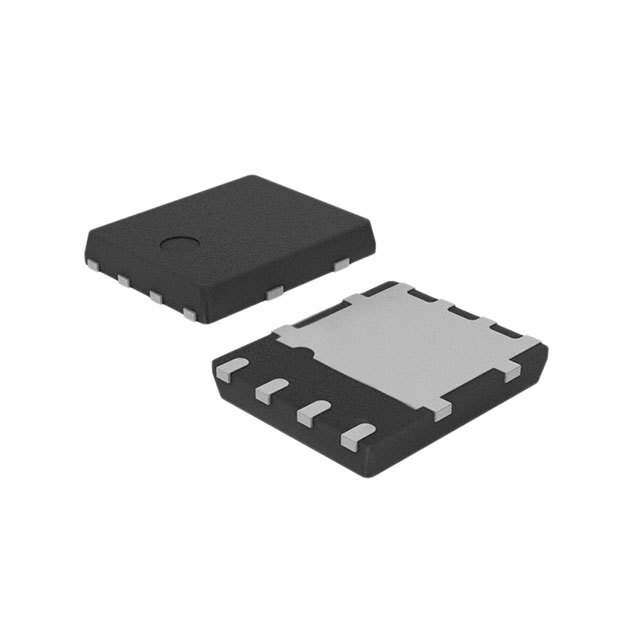
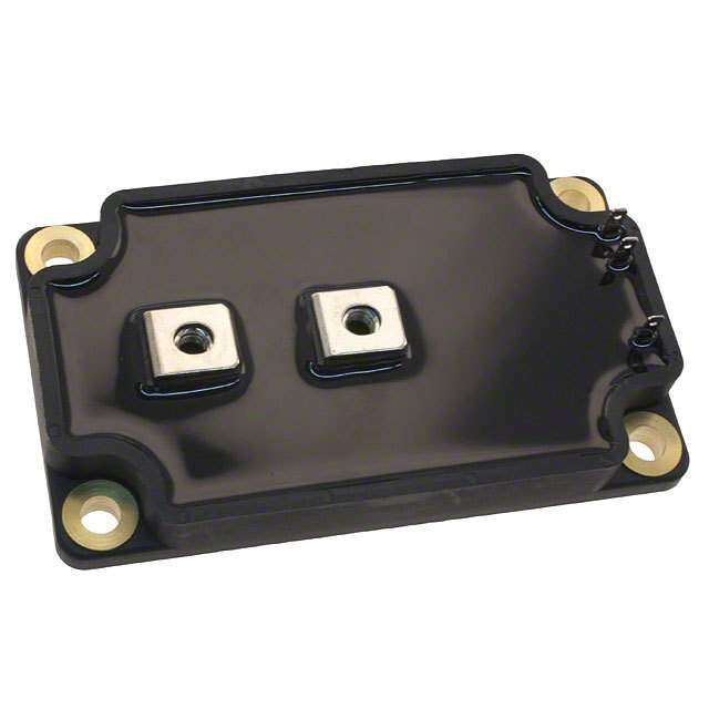
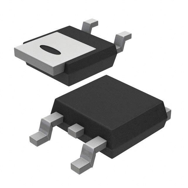
| 产品图片 |
|
| rohs | 符合RoHS无铅 / 符合限制有害物质指令(RoHS)规范要求 |
| 产品系列 | 晶体管,MOSFET,STMicroelectronics STL160N3LLH6DeepGATE™, STripFET™ VI |
| 数据手册 | |
| 产品型号 | STL160N3LLH6 |
| Pd-PowerDissipation | 80 W |
| Pd-功率耗散 | 80 W |
| Qg-GateCharge | 61.5 nC |
| Qg-栅极电荷 | 61.5 nC |
| RdsOn-Drain-SourceResistance | 1.1 mOhms |
| RdsOn-漏源导通电阻 | 1.1 mOhms |
| Vds-Drain-SourceBreakdownVoltage | 30 V |
| Vds-漏源极击穿电压 | 30 V |
| Vgs-Gate-SourceBreakdownVoltage | 20 V |
| Vgs-栅源极击穿电压 | 20 V |
| Vgsth-Gate-SourceThresholdVoltage | 1 V |
| Vgsth-栅源极阈值电压 | 1 V |
| 上升时间 | 32 ns |
| 下降时间 | 54 ns |
| 不同Id时的Vgs(th)(最大值) | 1V @ 250µA |
| 不同Vds时的输入电容(Ciss) | 6375pF @ 25V |
| 不同Vgs时的栅极电荷(Qg) | 61.5nC @ 4.5V |
| 不同 Id、Vgs时的 RdsOn(最大值) | 1.3 毫欧 @ 17.5A,10V |
| 产品种类 | MOSFET |
| 供应商器件封装 | PowerFlat™(5x6) |
| 其它名称 | 497-11204-2 |
| 其它有关文件 | http://www.st.com/web/catalog/sense_power/FM100/CL824/SC1164/PF250434?referrer=70071840 |
| 功率-最大值 | 80W |
| 包装 | 带卷 (TR) |
| 商标 | STMicroelectronics |
| 安装类型 | 表面贴装 |
| 安装风格 | SMD/SMT |
| 封装 | Reel |
| 封装/外壳 | 8-PowerVDFN |
| 封装/箱体 | PowerFLAT-8 5x6 |
| 工厂包装数量 | 3000 |
| 晶体管极性 | N-Channel |
| 标准包装 | 3,000 |
| 漏源极电压(Vdss) | 30V |
| 电流-连续漏极(Id)(25°C时) | 160A (Tc) |
| 系列 | STL160N3LLH6 |


- 商务部:美国ITC正式对集成电路等产品启动337调查
- 曝三星4nm工艺存在良率问题 高通将骁龙8 Gen1或转产台积电
- 太阳诱电将投资9.5亿元在常州建新厂生产MLCC 预计2023年完工
- 英特尔发布欧洲新工厂建设计划 深化IDM 2.0 战略
- 台积电先进制程称霸业界 有大客户加持明年业绩稳了
- 达到5530亿美元!SIA预计今年全球半导体销售额将创下新高
- 英特尔拟将自动驾驶子公司Mobileye上市 估值或超500亿美元
- 三星加码芯片和SET,合并消费电子和移动部门,撤换高东真等 CEO
- 三星电子宣布重大人事变动 还合并消费电子和移动部门
- 海关总署:前11个月进口集成电路产品价值2.52万亿元 增长14.8%


PDF Datasheet 数据手册内容提取
STL160N3LLH6 N-channel 30 V, 0.0011 Ω typ., 45 A STripFET™ H6 Power MOSFET in a PowerFLAT™ 5x6 package − Datasheet production data Features Order code V R max I DS DS(on) D STL160N3LLH6 30 V 0.0013 Ω 45 A (1) 1. The value is rated according to R thj-pcb 1 2 • Very low on-resistance 3 4 • Very low switching gate charge • High avalanche ruggedness PowerFLAT™5x6 • Low gate drive power loss Applications Figure 1. Internal schematic diagram • Switching applications (cid:39)(cid:11)(cid:24)(cid:15)(cid:3)(cid:25)(cid:15)(cid:3)(cid:26)(cid:15)(cid:3)(cid:27)(cid:12) Description This device is an N-channel Power MOSFET developed using the 6th generation of STripFET™ technology, with a new trench gate structure. The resulting Power MOSFET exhibits a very low (cid:42)(cid:11)(cid:23)(cid:12) R in all packages. DS(on) (cid:54)(cid:11)(cid:20)(cid:15)(cid:3)(cid:21)(cid:15)(cid:3)(cid:22)(cid:12) (cid:36)(cid:48)(cid:19)(cid:20)(cid:23)(cid:26)(cid:24)(cid:89)(cid:22) Table 1. Device s ummary Order code Marking Package Packaging STL160N3LLH6 160N3LH6 PowerFLAT™ 5x6 Tape and reel September 2014 DocID18223 Rev 6 1/15 This is information on a product in full production. www.st.com 15
Contents STL160N3LLH6 Contents 1 Electrical ratings . . . . . . . . . . . . . . . . . . . . . . . . . . . . . . . . . . . . . . . . . . . . 3 2 Electrical characteristics . . . . . . . . . . . . . . . . . . . . . . . . . . . . . . . . . . . . . 4 2.1 Electrical characteristics (curves) . . . . . . . . . . . . . . . . . . . . . . . . . . . . 6 3 Test circuits . . . . . . . . . . . . . . . . . . . . . . . . . . . . . . . . . . . . . . . . . . . . . . 8 4 Package mechanical data . . . . . . . . . . . . . . . . . . . . . . . . . . . . . . . . . . . . . 9 5 Packaging mechanical data . . . . . . . . . . . . . . . . . . . . . . . . . . . . . . . . . . 12 6 Revision history . . . . . . . . . . . . . . . . . . . . . . . . . . . . . . . . . . . . . . . . . . . 14 2/15 DocID18223 Rev 6
STL160N3LLH6 Electrical ratings 1 Electrical ratings Table 2. Absolute maximum ratings Symbol Parameter Value Unit V Drain-source voltage 30 V DS V Gate-source voltage ± 20 V GS I (1) Drain current (continuous) at T = 25 °C 240 A D C I (1) Drain current (continuous) at T = 100 °C 170 A D C I (1),(3) Drain current (pulsed) 960 A DM I (2) Drain current (continuous) at T = 25 °C 45 A D pcb I (2) Drain current (continuous) at T =100 °C 32 A D pcb I (2),(3) Drain current (pulsed) 180 A DM P (1) Total dissipation at T = 25 °C 136 W TOT C P (2) Total dissipation at T = 25 °C 4.8 W TOT pcb T Operating junction temperature j -55 to 175 °C T Storage temperature stg 1. The value is rated according to R . thj-c 2. The value is rated according to R thj-pcb. 3. Pulse width limited by safe operating area. Table 3. Thermal data Symbol Parameter Value Unit R Thermal resistance junction-case 1.1 °C/W thj-case R (1) Thermal resistance junction-pcb 31.3 °C/W thj-pcb 1. When mounted on FR-4 board of 1inch², 2oz Cu, t < 10 sec. Table 4. Avalanche data Symbol Parameter Value Unit Not-repetitive avalanche current I 35 A AV (pulse width limited by T max) j Single pulse avalanche energy E 900 mJ AS (starting T = 25 °C, I = I ) J D AV DocID18223 Rev 6 3/15
Electrical characteristics STL160N3LLH6 2 Electrical characteristics (T = 25 °C unless otherwise specified). CASE Table 5. On/off states Symbol Parameter Test conditions Min. Typ. Max. Unit Drain-source breakdown V V = 0, I = 250 µA 30 V (BR)DSS voltage GS D Zero gate voltage drain VGS = 0, VDS = 30 V 1 µA I DSS current V = 30 V at T = 125 °C 10 µA DS C IGSS Gate body leakage current VDS = 0, VGS = ±20 V ±100 nA V Gate threshold voltage V = V , I = 250 µA 1 V GS(th) DS GS D Static drain-source on- VGS= 10 V, ID= 17.5 A 0.0011 0.0013 Ω R DS(on) resistance V = 4.5 V, I = 17.5 A 0.0016 0.0020 Ω GS D Table 6. Dynamic Symbol Parameter Test conditions Min. Typ. Max. Unit C Input capacitance - 6375 - pF iss C Output capacitance V =0, V = 25 V, - 1230 - pF oss GS DS f=1 MHz Reverse transfer C - 675 - pF rss capacitance Q Total gate charge - 61.5 - nC g V =15 V, I = 35 A DD D Q Gate-source charge V =4.5 V - 20 nC gs GS (see Figure 14) Q Gate-drain charge - 24 nC gd f = 1 MHz, gate DC Bias = 0, R Gate input resistance - 1.4 - Ω g test signal level = 20 mV, I = 0 D Table 7. Switching times Symbol Parameter Test conditions Min. Typ. Max. Unit t Turn-on delay time - 22.5 - ns d(on) V =15 V, I = 17.5 A, t Rise time DD D - 32 - ns r R =4.7 Ω, V =10 V G GS t Turn-off delay time - 107.5 - ns d(off) (see Figure 13) t Fall time - 54 - ns f 4/15 DocID18223 Rev 6
STL160N3LLH6 Electrical characteristics Table 8. Source drain diode Symbol Parameter Test conditions Min. Typ. Max. Unit I Source-drain current - 45 A SD I (1) Source-drain current (pulsed) - 180 A SDM V (2) Forward on voltage V =0, I = 35 A - 1.1 V SD GS SD t Reverse recovery time - 37.2 ns rr I = 35 A, SD Q Reverse recovery charge di/dt = 100 A/µs, - 36 nC rr V =25 V I Reverse recovery current DD - 1.9 A RRM 1. Pulse width limited by safe operating area. 2. Pulsed: pulse duration=300µs, duty cycle 1.5%. DocID18223 Rev 6 5/15
Electrical characteristics STL160N3LLH6 2.1 Electrical characteristics (curves) Figure 2. Safe operating area Figure 3. Thermal impedance ID AM08599v1 K AM15985v1 1(0A0) OpLeirmaittieodn ibny thmisa xa rReDa Si(son) TSTpji=nc1gb7l=e5 2p°5Cu°lCse 10-1 δ=0.5 00..12 0.05 0.02 0.01 10 10-2 pcb 10ms 1 100ms 10-3 Single pulse 1s 0.1 10-4 0.1 1 10 VDS(V) 10-6 10-5 10-4 10-3 10-2 10-1 100tp(s) Figure 4. Output characteristics Figure 5. Transfer characteristics AM08600v1 AM08601v1 ID(A) ID (A) VDS=2V 180 160 80 140 70 120 60 4V 100 50 3V 80 40 60 30 40 20 20 10 0 0 0 0.5 1.0 1.5 2.0 2.5 VDS(V) 0 1 2 3 4 VGS(V) Figure 6. Normalized V vs temperature Figure 7. Static drain-source on-resistance (BR)DSS V(BR)DSS AM08602v1 RDS(on) AM08603v1 (norm) (mΩ) VGS=10V 1.10 1.15 1.05 1.10 1.00 1.05 0.95 1.00 0.90 0.95 -75 -25 25 75 125 175 TJ(°C) 0 5 10 15 20 25 30 35 40 ID(A) 6/15 DocID18223 Rev 6
STL160N3LLH6 Electrical characteristics Figure 8. Gate charge vs gate-source voltage Figure 9. Capacitance variations VGS AM08604v1 C (pF) AM08605v1 (V) 12 VDD=15V 9000 ID=35A 8000 10 7000 Ciss 6000 8 5000 6 4000 4 3000 2000 2 Coss 1000 Crss 0 0 0 20 40 60 80 100 120 Qg(nC) 0 5 10 15 20 25 30 VDS(V) Figure 10. Normalized gate threshold voltage vs Figure 11. Normalized on-resistance vs temperature temperature VGS(th) AM08606v1 RDS(on) AM08607v1 (norm) (norm) 1.8 1.2 1.6 1.0 1.4 0.8 1.2 1.0 0.6 0.8 0.4 0.6 0.2 0.4 -75 -25 25 75 125 175 TJ(°C) -75 -25 25 75 125 175 TJ(°C) Figure 12. Source-drain diode forward characteristics VSD AM08608v1 (V) TJ=-55°C 0.9 0.8 0.7 TJ=25°C 0.6 0.5 TJ=175°C 0.4 0.3 0 5 10 15 20 25 30 35 40 ISD(A) DocID18223 Rev 6 7/15
Test circuits STL160N3LLH6 3 Test circuits Figure 13. Switching times test circuit for Figure 14. Gate charge test circuit resistive load VDD 12V 47kΩ 1kΩ 100nF RL 2μ20F0 3μ.F3 VDD IG=CONST VD Vi=20V=VGMAX 100Ω D.U.T. VGS 2200 RG D.U.T. μF 2.7kΩ VG PW 47kΩ 1kΩ PW AM01468v1 AM01469v1 Figure 15. Test circuit for inductive load Figure 16. Unclamped inductive load test circuit switching and diode recovery times L A A A D FAST L=100μH VD G D.U.T. DIODE 2200 3.3 μF μF VDD S B 3.3 1000 B B μF μF 25Ω D VDD ID G RG S Vi D.U.T. Pw AM01470v1 AM01471v1 Figure 17. Unclamped inductive waveform Figure 18. Switching time waveform V(BR)DSS ton toff VD tdon tr tdoff tf 90% 90% IDM 10% ID 0 10% VDS VDD VDD 90% VGS AM01472v1 0 10% AM01473v1 8/15 DocID18223 Rev 6
STL160N3LLH6 Package mechanical data 4 Package mechanical data In order to meet environmental requirements, ST offers these devices in different grades of ECOPACK® packages, depending on their level of environmental compliance. ECOPACK® specifications, grade definitions and product status are available at: www.st.com. ECOPACK® is an ST trademark. DocID18223 Rev 6 9/15
Package mechanical data STL160N3LLH6 Figure 19. PowerFLAT™ 5x6 type S-C mechanical data (cid:37)(cid:82)(cid:87)(cid:87)(cid:82)(cid:80)(cid:3)(cid:89)(cid:76)(cid:72)(cid:90) (cid:24) (cid:27) (cid:51)(cid:76)(cid:81)(cid:3)(cid:20) (cid:76)(cid:71)(cid:72)(cid:81)(cid:87)(cid:76)(cid:73)(cid:76)(cid:70)(cid:68)(cid:87)(cid:76)(cid:82)(cid:81) (cid:23) (cid:20) (cid:54)(cid:76)(cid:71)(cid:72)(cid:3)(cid:89)(cid:76)(cid:72)(cid:90) (cid:51)(cid:76)(cid:81)(cid:3)(cid:20)(cid:3) (cid:76)(cid:71)(cid:72)(cid:81)(cid:87)(cid:76)(cid:73)(cid:76)(cid:70)(cid:68)(cid:87)(cid:76)(cid:82)(cid:81) (cid:23) (cid:20) (cid:15) (cid:24) (cid:27) (cid:55)(cid:82)(cid:83)(cid:3)(cid:89)(cid:76)(cid:72)(cid:90) (cid:27)(cid:21)(cid:22)(cid:20)(cid:27)(cid:20)(cid:26)(cid:66)(cid:44)(cid:66)(cid:38) 10/15 DocID18223 Rev 6
STL160N3LLH6 Package mechanical data Table 9. PowerFLAT™ 5x6 type S-C mechanical data mm Dim. Min. Typ. Max. A 0.80 1.00 A1 0.02 0.05 A2 0.25 b 0.30 0.50 D 5.20 E 6.15 D2 4.11 4.31 E2 3.50 3.70 e 1.27 e1 0.65 L 0.715 1.015 K 1.05 1.35 E3 2.35 2.55 E4 0.40 0.60 E5 0.08 0.28 Figure 20. PowerFLAT™ 5x6 recommended footprint (dimensions in mm) Footprint DocID18223 Rev 6 11/15
Packaging mechanical data STL160N3LLH6 5 Packaging mechanical data Figure 21. PowerFLAT™ 5x6 tape(a) P2 P0 (0.T30 ±0.05) 2.0 ±0.1 (I) 4.0±0. 1 (II) Do E1 Ø1.55±0.05 Y 1.75±0.1 CL Bo (5.30±0.1) DØ11.5 MIN. REF 0.20 F(5.50±0.1)(III) W(12.00±0.3) REF.R0.50 Y P1(8.00±0.1) Ao(6.30±0.1) Ko (1.20±0.1) SECTION Y-Y (I) Measured from centerline of sprocket hole Base and bulk quantity 3000 pcs to centerline of pocket. (II) Cumulative tolerance of 10 sprocket holes is ± 0.20 . (III)Measured from centerline of sprocket hole to centerline of pocket. 8234350_Tape_rev_C Figure 22. PowerFLAT™ 5x6 package orientation in carrier tape Pin 1 identification a. All dimensions are in millimeters. 12/15 DocID18223 Rev 6
STL160N3LLH6 Packaging mechanical data Figure 23. PowerFLAT™ 5x6 reel R0.60 W3 PART NO. 11.9/15.4 1.90 2.50 W2 18.4 (max) R25.004.00 1 7Ø8N(±2.0) ATTENTIONOBSERVE PRECAUTIONSFOR HANDLING ELECTROSTATICSENSITIVE DEVICES 3 3 A0 (+0/-4.0) 2.50 77 ESD LOGO W1 12.4 (+2/-0) 60SP ØA 128 R1.10 Ø21.2 2.20 All dimensions are in millimeters 13.00 CORE DETAIL 8234350_Reel_rev_C DocID18223 Rev 6 13/15
Revision history STL160N3LLH6 6 Revision history Table 10. Document revision history Date Revision Changes 10-Nov-2010 1 First release. Section4: Package mechanical data has been updated. 10-Nov-2011 2 Minor text changes. – Modified: I in the title and in the Features Table, Table5, 6 and 7 D – Modified: values on the Table2, R on the Table3, max thj-case values for the I and I on Table8 SD SDM 31-Jul-2013 3 – Updated: Section4: Package mechanical data – Inserted: Section5: Packaging mechanical data – Modified: Figure13, 14, 15 and 16 – Minor text changes – Modified: drain current (continuous) at T = 100 °C value and drain C current (continuous) at T =100 °C value pcb – Modified: test conditions of R DS(on) – Modified: I in Table6 and 7 D 09-Aug-2013 4 – Modified: I in Table8 SD – Modified: Figure2, 3, 4, 5, 7, 12, 13, 14, 15 and 16 – Updated: Section4: Package mechanical data – Minor text changes – Modified: marking in Table1 24-Sep-2013 5 – Minor text changes – Modified: title – Modified: Features 23-Sep-2014 6 – Modified: Description – Updated: Section4: Package mechanical data – Minor text changes 14/15 DocID18223 Rev 6
STL160N3LLH6 IMPORTANT NOTICE – PLEASE READ CAREFULLY STMicroelectronics NV and its subsidiaries (“ST”) reserve the right to make changes, corrections, enhancements, modifications, and improvements to ST products and/or to this document at any time without notice. Purchasers should obtain the latest relevant information on ST products before placing orders. ST products are sold pursuant to ST’s terms and conditions of sale in place at the time of order acknowledgement. Purchasers are solely responsible for the choice, selection, and use of ST products and ST assumes no liability for application assistance or the design of Purchasers’ products. No license, express or implied, to any intellectual property right is granted by ST herein. Resale of ST products with provisions different from the information set forth herein shall void any warranty granted by ST for such product. ST and the ST logo are trademarks of ST. All other product or service names are the property of their respective owners. Information in this document supersedes and replaces information previously supplied in any prior versions of this document. © 2014 STMicroelectronics – All rights reserved DocID18223 Rev 6 15/15