ICGOO在线商城 > 分立半导体产品 > 晶体管 - UGBT,MOSFET - 单 > STGW40NC60V
 Datasheet下载
- 型号: STGW40NC60V
- 制造商: STMicroelectronics
- 库位|库存: xxxx|xxxx
- 要求:
| 数量阶梯 | 香港交货 | 国内含税 |
| +xxxx | $xxxx | ¥xxxx |
查看当月历史价格
查看今年历史价格
STGW40NC60V产品简介:
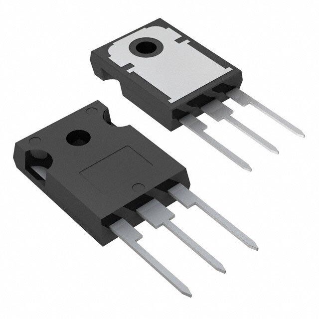
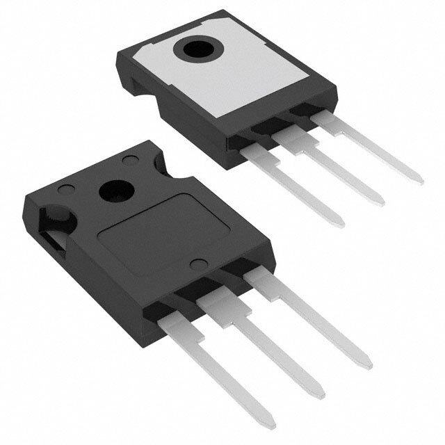
ICGOO电子元器件商城为您提供STGW40NC60V由STMicroelectronics设计生产,在icgoo商城现货销售,并且可以通过原厂、代理商等渠道进行代购。 STGW40NC60V价格参考。STMicroelectronicsSTGW40NC60V封装/规格:晶体管 - UGBT,MOSFET - 单, IGBT 600V 80A 260W Through Hole TO-247-3。您可以下载STGW40NC60V参考资料、Datasheet数据手册功能说明书,资料中有STGW40NC60V 详细功能的应用电路图电压和使用方法及教程。
| 参数 | 数值 |
| 25°C时Td(开/关)值 | 43ns/140ns |
| 产品目录 | |
| Current-CollectorPulsed(Icm) | 200A |
| 描述 | IGBT 600V 80A 260W TO247IGBT 晶体管 N-Ch 600 Volt 50 Amp |
| 产品分类 | IGBT - 单路分离式半导体 |
| GateCharge | 214nC |
| IGBT类型 | - |
| 品牌 | STMicroelectronics |
| 产品手册 | |
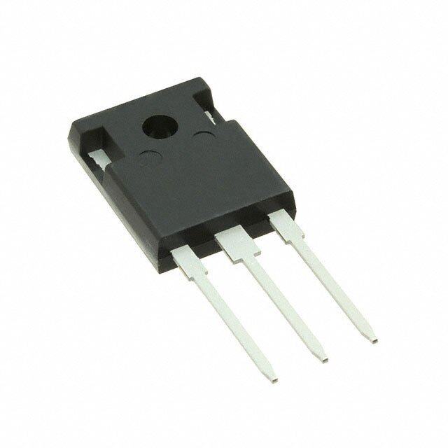
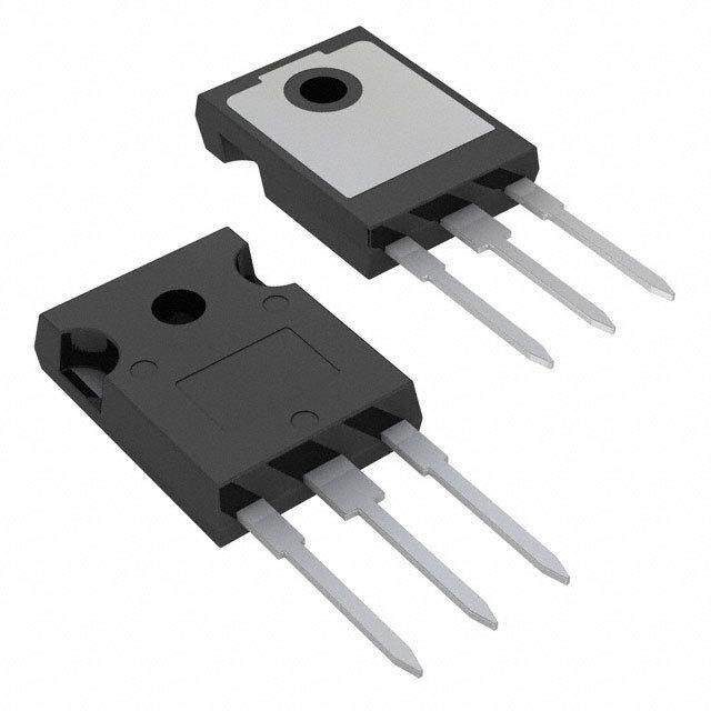
| 产品图片 |
|
| rohs | 符合RoHS无铅 / 符合限制有害物质指令(RoHS)规范要求 |
| 产品系列 | 晶体管,IGBT 晶体管,STMicroelectronics STGW40NC60VPowerMESH™ |
| 数据手册 | |
| 产品型号 | STGW40NC60V |
| SwitchingEnergy | 330µJ (开), 720µJ (关) |
| TestCondition | 390V, 40A, 3.3 欧姆, 15V |
| 不同 Vge、Ic时的 Vce(on) | 2.5V @ 15V,40A |
| 产品种类 | IGBT 晶体管 |
| 供应商器件封装 | TO-247-3 |
| 其它名称 | 497-4358-5 |
| 其它有关文件 | http://www.st.com/web/catalog/sense_power/FM100/CL826/SC68/PF68809?referrer=70071840 |
| 功率-最大值 | 260W |
| 功率耗散 | 260 W |
| 包装 | 管件 |
| 反向恢复时间(trr) | - |
| 商标 | STMicroelectronics |
| 在25C的连续集电极电流 | 100 A |
| 安装类型 | 通孔 |
| 安装风格 | Through Hole |
| 封装 | Tube |
| 封装/外壳 | TO-247-3 |
| 封装/箱体 | TO-247-3 |
| 工厂包装数量 | 30 |
| 最大工作温度 | + 150 C |
| 最小工作温度 | - 55 C |
| 栅极/发射极最大电压 | +/- 20 V |
| 栅极—射极漏泄电流 | +/- 100 nA |
| 标准包装 | 30 |
| 特色产品 | http://www.digikey.cn/product-highlights/zh/tailless-600-v-igbt-v-series/51749 |
| 电压-集射极击穿(最大值) | 600V |
| 电流-集电极(Ic)(最大值) | 80A |
| 系列 | STGW40NC60V |
| 输入类型 | 标准 |
| 配置 | Single |
| 集电极—发射极最大电压VCEO | 600 V |
| 集电极—射极饱和电压 | 2.5 V |
| 集电极最大连续电流Ic | 80 A |


PDF Datasheet 数据手册内容提取
STGW40NC60V N-CHANNEL 50A - 600V - TO-247 Very Fast PowerMESH™ IGBT Table 1: General Features Figure 1: Package TYPE VCES VCE(sat) (Max) IC @25°C @100°C STGW40NC60V 600 V < 2.5 V 50 A ) s (cid:1) HIGH CURRENT CAPABILITY t( c (cid:1) HIGH FREQUENCY OPERATION UP TO u 50 KHz d (cid:1) LOSSES INCLUDE DIODE RECOVERY o3 ENERGY P r2 1 (cid:1) OFF LOSSES INCLUDE TAIL CURRENT TOe- 247 (cid:1) LOWER CRES / CIES RATIO t e (cid:1) NEW GENERATION PRODUCTS WITH l TIGHTER PARAMETER DISTRUBUTION Weight: 4.41ogr ± 0.01 s Max Clibp Pressure: 150 N/mm2 DESCRIPTION O Using the latest high voltage technology based on -F igure 2: Internal Schematic Diagram a patented strip layout, STMicroelectronics has ) designed an advanced family of IGBTs, the Pows- erMESH™ IGBTs, with outstanding performanc(es. t The suffix “V” identifies a family optimized fcor high u frequency. d o r P APPLICATIONS (cid:1) HIGH FREQUENCY eIN VERTERS (cid:1) SMPS and PFC eINt BOTH HARD SWITCH AND RESONANT lTOPOLOGIES o (cid:1) UPS s (cid:1) MOTObR DRIVERS O Table 2: Order Codes SALES TYPE MARKING PACKAGE PACKAGING STGW40NC60V GW40NC60V TO-247 TUBE Rev. 10 July 2004 1/10
STGW40NC60V Table 3: Absolute Maximum ratings Symbol Parameter Value Symbol VCES Collector-Emitter Voltage (VGS = 0) 600 V VECR Reverse Battery Protection 20 V VGE Gate-Emitter Voltage ± 20 V IC Collector Current (continuous) at 25°C (#) 80 A IC Collector Current (continuous) at 100°C (#) 50 A ICM (1) Collector Current (pulsed) 200 A PTOT Total Dissipation at TC = 25°C 260 W Derating Factor 2.08 W/°C ) s Tstg Storage Temperature t( – 55 to 150 c°C Tj Operating Junction Temperature u (1)Pulse width limited by max. junction temperature. d o r Table 4: Thermal Data P e Min. Typ. Max. Unit t e Rthj-case Thermal Resistance Junction-case 0.48 °C/W l o Rthj-amb Thermal Resistance Junction-ambient 50 °C/W s TL Maximum Lead Temperature for Soldering Purpose b 300 °C (1.6 mm from case, for 10 sec.) O ELECTRICAL CHARACTERISTICS (TCASE =25°C UN-L ESS OTHERWISE SPECIFIED) Table 5: Off ) s Symbol Parameter (Test Conditions Min. Typ. Max. Unit t c VBR(CES) Collectro-Emitter Breakdown uIC = 1 mA, VGE = 0 600 V Voltage d ICES Collector-Emitter Leakaoge VGE = Max Rating Current (VCE = 0)P r Tc=25°C 10 µA Tc=125°C 1 mA e IGES Gate-Emtitter Leakage VGE = ± 20 V , VCE = 0 ± 100 nA Currenet (VCE = 0) l o Table 6: Ons b SyOmbol Parameter Test Conditions Min. Typ. Max. Unit VGE(th) Gate Threshold Voltage VCE= VGE, IC= 250 µA 3.75 5.75 V VCE(SAT) Collector-Emitter Saturation VGE= 15 V, IC= 40A, Tj= 25°C 1.9 2.5 V Voltage VGE= 15 V, IC= 40A, 1.7 V Tj= 125°C (#) Calculated according to the iterative formula: T –T I (T ) = ------------------------------------J---M------A-----X--------------C---------------------------------- C C RTHJ–C×VCESAT(MAX)(TC,IC) 2/10
STGW40NC60V ELECTRICAL CHARACTERISTICS (CONTINUED) Table 7: Dynamic Symbol Parameter Test Conditions Min. Typ. Max. Unit gfs(1) Forward Transconductance VCE = 15 V, IC= 20 A 20 S Cies Input Capacitance VCE = 25V, f = 1 MHz, VGE = 0 4550 pF Coes Output Capacitance 350 pF Cres Reverse Transfer 105 pF Capacitance Qg Total Gate Charge VCE = 390 V, IC = 40 A, 214 nC Qge Gate-Emitter Charge VGE = 15V, 30 nC Qgc Gate-Collector Charge (see Figure 20) 96 nC ICL Turn-Off SOA Minimum Vclamp = 480 V , Tj = 150°C 200 A s ) Current RG = 100 Ω, VGE= 15V t( c Table 8: Switching On u Symbol Parameter Test Conditions Min. Typ. Mdax. Unit o td(on) Turn-on Delay Time VCC = 390 V, IC = 40 A 43r ns tr Current Rise Time RG=3.3Ω, VGE= 15V, Tj= 25°C 1P7 ns (di/dt)on Turn-on Current Slope (see Figure 18) e 2060 A/µs Eon (2) Turn-on Switching Losses t 330 450 µJ e td(on) Turn-on Delay Time VCC = 390 V, IC = 40 A ol 42 ns tr Current Rise Time RG=3.3Ω, VGE= 15V, Tj= s 19 ns (di/dt)on Turn-on Current Slope 125°C b 1900 A/µs Eon (2) Turn-on Switching Losses (see Figure 18) O 640 µJ 2) Eon is the turn-on losses when a typical diode is used in the test circuit in figure 2. If the IGBT is offered in a package with a co-pack diode, the co-pack diode is used as external diode. IGBTs & DIODE are at th e -same temperature (25°C and 125°C) Table 9: Switching Off ) s ( Symbol Parameter t Test Conditions Min. Typ. Max. Unit c tr(Voff) Off Voltage Rise Time u Vcc = 390 V, IC = 40 A, 25 ns td(off) Turn-off Delay Time o d RTJG =E =25 3 °.3C Ω , VGE = 15 V 140 ns tf Current Fall TimeP r (see Figure 18) 45 ns Eoff (3) Turn-off Sweit ching Loss 720 970 µJ Ets Total Sewtitching Loss 1050 1420 µJ tr(Voff) Ooflf Voltage Rise Time Vcc = 390 V, IC = 40 A, 60 ns td(off)b s Turn-off Delay Time RTjG =E 1=2 35. 3°C Ω , VGE = 15 V 170 ns Otf Current Fall Time (see Figure 18) 77 ns Eoff (3) Turn-off Switching Loss 1400 µJ Ets Total Switching Loss 2040 µJ (3)Turn-off losses include also the tail of the collector current. 3/10
STGW40NC60V Figure 3: Output Characteristics Figure 6: Transfer Characteristics ) s ( t c u d o r Figure 4: Transconductance Figure 7: Collector-EmitterP On Voltage vs Tem- perature e t e l o s b O - ) s ( t c u d o r P e t Figure 5: Collectoer-Emitter On Voltage vs Col- Figure 8: Normalized Gate Threshold vs Tem- lector Currentol perature s b O 4/10
STGW40NC60V Figure 9: Normalized Breakdown Voltage vs Figure 12: Gate Charge vs Gate-Emitter Volt- Temperature age ) s ( t c u d o r Figure 10: Capacitance Variations Figure 13: Total SwitchingP Losses vs Temper- ature e t e l o s b O - ) s ( t c u d o r P e t Figure 11: Total Sewitching Losses vs Gate Re- Figure 14: Total Switching Losses vs Collector sistance ol Current s b O 5/10
STGW40NC60V Figure 15: Thermal Impedance Figure 17: Ic vs Frequency ) s ( t c u d o r Figure 16: Turn-Off SOA For a fast IGBT suitable for Phigh frequency appli- cations, the typical collec tor current vs. maximum e operating frequency curve is reported. That fre- t quency is defined aes follows: l fo = (P - P ) / (E + E ) MAX D C ON OFF s 1) The maximum power dissipation is limited by b maximum junction to case thermal resistance: O PD = ∆T / RTHJ-C - ) considering ∆T = TJ - TC = 125 °C- 75 °C = 50°C s 2) The conduction losses are: ( ct PC = IC * VCE(SAT) * δ u with 50% of duty cycle, VCESAT typical value d @125°C. o r 3) Power dissipation during ON & OFF commuta- P tions is due to the switching frequency: e PSW = (EON + EOFF) * freq. e t 4) Typical values @ 125°C for switching losses are ol used (test conditions: VCE = 390V, VGE = 15V, s RG = 3.3 Ohm). Furthermore, diode recovery en- b ergy is included in the EON (see note 2), while the O tail of the collector current is included in the EOFF measurements (see note 3). 6/10
STGW40NC60V Figure 18: Test Circuit for Inductive Load Figure 20: Gate Charge Test Circuit Switching ) s ( t c u d o r P Figure 19: Switching Waveforms e t e l o s b O - ) s ( t c u d o r P e t e l o s b O 7/10
STGW40NC60V TO-247 MECHANICAL DATA mm. inch DIM. MIN. TYP MAX. MIN. TYP. MAX. A 4.85 5.15 0.19 0.20 A1 2.20 2.60 0.086 0.102 b 1.0 1.40 0.039 0.055 ) s b1 2.0 2.40 0.079 0.094 ( t b2 3.0 3.40 0.118 0.134 c u c 0.40 0.80 0.015 0.03 d D 19.85 20.15 0.781 0.793 o E 15.45 15.75 0.608 r0.620 P e 5.45 0.214 L 14.20 14.80 0.560 e 0.582 L1 3.70 4.30 0.14 t 0.17 e L2 18.50 l 0.728 o øP 3.55 3.65 0.140 0.143 s øR 4.50 5.50 0b.177 0.216 S 5.50 O 0.216 - ) s ( t c u d o r P e t e l o s b O 8/10
STGW40NC60V Table 10: Revision History Date Revision Description of Changes 13-Jul-2004 9 Stylesheet update. No content change 14-Jul-2004 10 Some datas have been updated ) s ( t c u d o r P e t e l o s b O - ) s ( t c u d o r P e t e l o s b O 9/10
STGW40NC60V ) s ( t c u d o r P e t e l o s b O - ) s ( t c u d o r P e t e l o s b O Information furnished is believed to be accurate and reliable. However, STMicroelectronics assumes no responsibility for the consequences of use of such information nor for any infringement of patents or other rights of third parties which may result from its use. No license is granted by implication or otherwise under any patent or patent rights of STMicroelectronics. Specifications mentioned in this publication are subject to change without notice. This publication supersedes and replaces all information previously supplied. STMicroelectronics products are not authorized for use as critical components in life support devices or systems without express written approval of STMicroelectronics. The ST logo is a registered trademark of STMicroelectronics All other names are the property of their respective owners © 2004 STMicroelectronics - All Rights Reserved STMicroelectronics GROUP OF COMPANIES Australia - Belgium - Brazil - Canada - China - Czech Republic - Finland - France - Germany - Hong Kong - India - Israel - Italy - Japan - Malaysia - Malta - Morocco - Singapore - Spain - Sweden - Switzerland - United Kingdom - United States. 10/10