ICGOO在线商城 > STGB30NC60KT4
- 型号: STGB30NC60KT4
- 制造商: STMicroelectronics
- 库位|库存: xxxx|xxxx
- 要求:
| 数量阶梯 | 香港交货 | 国内含税 |
| +xxxx | $xxxx | ¥xxxx |
查看当月历史价格
查看今年历史价格
STGB30NC60KT4产品简介:
ICGOO电子元器件商城为您提供STGB30NC60KT4由STMicroelectronics设计生产,在icgoo商城现货销售,并且可以通过原厂、代理商等渠道进行代购。 提供STGB30NC60KT4价格参考以及STMicroelectronicsSTGB30NC60KT4封装/规格参数等产品信息。 你可以下载STGB30NC60KT4参考资料、Datasheet数据手册功能说明书, 资料中有STGB30NC60KT4详细功能的应用电路图电压和使用方法及教程。
| 参数 | 数值 |
| 25°C时Td(开/关)值 | 29ns/120ns |
| 产品目录 | |
| Current-CollectorPulsed(Icm) | 125A |
| 描述 | IGBT 600V 60A 185W D2PAK |
| 产品分类 | IGBT - 单路 |
| GateCharge | 96nC |
| IGBT类型 | - |
| 品牌 | STMicroelectronics |
| 数据手册 | |
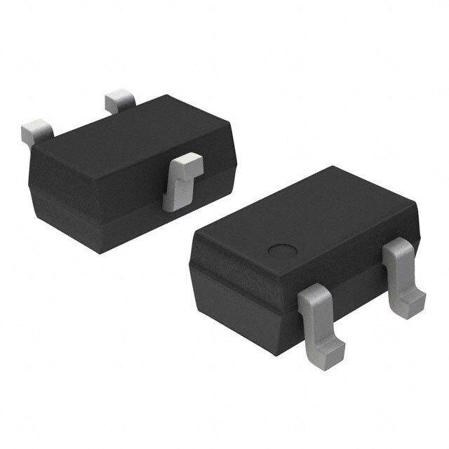
| 产品图片 |
|
| 产品型号 | STGB30NC60KT4 |
| rohs | 无铅 / 符合限制有害物质指令(RoHS)规范要求 |
| 产品系列 | PowerMESH™ |
| SwitchingEnergy | 350µJ (开), 435µJ (关) |
| TestCondition | 480V, 20A, 10 欧姆, 15V |
| 不同 Vge、Ic时的 Vce(on) | 2.7V @ 15V,20A |
| 产品目录页面 | |
| 供应商器件封装 | D2PAK |
| 其它名称 | 497-7009-2 |
| 其它有关文件 | http://www.st.com/web/catalog/sense_power/FM100/CL826/SC68/PF178486?referrer=70071840 |
| 功率-最大值 | 185W |
| 包装 | 带卷 (TR) |
| 反向恢复时间(trr) | - |
| 安装类型 | 表面贴装 |
| 封装/外壳 | TO-263-3,D²Pak(2 引线+接片),TO-263AB |
| 标准包装 | 1,000 |
| 特色产品 | http://www.digikey.cn/product-highlights/zh/tailless-600-v-igbt-v-series/51749 |
| 电压-集射极击穿(最大值) | 600V |
| 电流-集电极(Ic)(最大值) | 60A |
| 输入类型 | 标准 |



PDF Datasheet 数据手册内容提取
STGB30NC60K STGP30NC60K 30 A - 600 V - short circuit rugged IGBT Features ■ Low on-voltage drop (V ) CE(sat) ■ Low C / C ratio (no cross conduction res ies ) susceptibility) s ( ■ Short circuit withstand time 10 µs ct u d Applications 3 3 1 o 2 1 r ■ High frequency inverters D²PAK P TO-220 ■ Motor drivers e t e l Description o s b This IGBT utilizes the advanced PowerMESH™ O process resulting in an excellent trade-off between switching performance and low on-sta-te Figure 1. Internal schematic diagram ) behavior. s ( t c u d o r P e t e l o s b O Table 1. Device summary Order codes Marking Package Packaging STGB30NC60KT4 GB30NC60K D²PAK Tape and reel STGP30NC60K GP30NC60K TO-220 Tube March 2008 Rev 2 1/15 www.st.com 15
Contents STGB30NC60K - STGP30NC60K Contents 1 Electrical ratings . . . . . . . . . . . . . . . . . . . . . . . . . . . . . . . . . . . . . . . . . . . . 3 2 Electrical characteristics . . . . . . . . . . . . . . . . . . . . . . . . . . . . . . . . . . . . . 4 2.1 Electrical characteristics (curves) . . . . . . . . . . . . . . . . . . . . . . . . . . . . 6 3 Test circuit . . . . . . . . . . . . . . . . . . . . . . . . . . . . . . . . . . . . . . . . . . . . . . . . 9 ) s 4 Package mechanical data . . . . . . . . . . . . . . . . . . . . . . . . . . . . . . . (. . . . . 10 t c u d 5 Packaging mechanical data . . . . . . . . . . . . . . . . . . . . . . . . . . . . . . . . . . 13 o r P 6 Revision history . . . . . . . . . . . . . . . . . . . . . . . . . . . . . . . . . . . . . . . . . . . 14 e t e l o s b O - ) s ( t c u d o r P e t e l o s b O 2/15
STGB30NC60K - STGP30NC60K Electrical ratings 1 Electrical ratings Table 2. Absolute maximum ratings Symbol Parameter Value Unit V Collector-emitter voltage (V = 0) 600 V CES GE I (1) Collector current (continuous) at T = 25°C 60 A C C I (1) Collector current (continuous) at T = 100°C 26 A C C I (2) Turn-off latching current 125 A CL ) I (3) Pulsed collector current 125 s A CP ( t V Gate-emitter voltage ±20 c V GE u P Total dissipation at T = 25°C 1d85 W TOT C o Short circuit withstand time, V = 0.5V r t CE (BR)CES P 10 µs scw T = 125°C, R = 10 Ω, V = 12 V j G GE e Tj Operating junction temperature t – 55 to 150 °C e 1. Calculated according to the iterative formula: ol s b O I (T ) =- ---------------------------T----J--(--M-----A---X---)----–----T----c---------------------------- c )c Rthj–c× VCE(sat)(MAX)⋅ (Tc,Ic) s ( t c u d 2. Vclamp = 80%o,(VCES), Tj =150°C, RG = 10 Ω, VGE = 15 V 3. Pulse widrth limited by max. junction temperature allowed P e Ttable 3. Thermal resistance e l o Symbol Parameter Value Unit s b R Thermal resistance junction-case max. 0.675 °C/W thj-case O R Thermal resistance junction-ambient max. 62.5 °C/W thj-amb 3/15
Electrical characteristics STGB30NC60K - STGP30NC60K 2 Electrical characteristics (T =25°C unless otherwise specified) CASE Table 4. Static Symbol Parameter Test conditions Min. Typ. Max. Unit Collector-emitter breakdown V(BR)CES voltage (V = 0) IC= 1 mA 600 V GE V = 15 V, I = 20 A 2.1 2.7 V GE C VCE(SAT) Cvooltllaegcetor-emitter saturation VGE= 15 V, IC= 20 A, s ) Tc= 125°C 1.9 ( V t c Collector cut-off current V = 600 V u 150 µA I CE CES (VGE = 0) VCE = 600 V, TC= 125°C o d 1 mA VGE(th) Gate threshold voltage VCE= VGE, IC= 250 µA P r 4.5 6.5 V Gate-emitter cut-off e IGES current (VCE = 0) VGE= ±20 V e t ±100 nA l o g (1) Forward transconductance V = 15 V I = 20 A 15 S fs CE s , C b 1. Pulsed: Pulse duration = 300 µs, duty cycle 1O.5% - Table 5. Dynamic ) s Symbol Parame(ter Test conditions Min. Typ. Max. Unit t c Input capaucitance Cies d 2170 pF Output capacitance Coes o VCE = 25 V, f = 1 MHz, VGE= 0 230 pF rReverse transfer C P 46 pF res capacitance e Q Total gate charge V = 480 V, I = 20 A, 96 nC t g CE C e Q Gate-emitter charge V = 15 V 18 nC l ge GE o Q Gate-collector charge (see Figure 17) 46 nC s gc b O 4/15
STGB30NC60K - STGP30NC60K Electrical characteristics Table 6. Switching on/off (inductive load) Symbol Parameter Test conditions Min. Typ. Max. Unit t Turn-on delay time V = 480 V, I = 20 A 29 ns d(on) CC C t Current rise time R =10 Ω, V = 15 V 12 ns r G GE (di/dt) Turn-on current slope (see Figure 16) 1520 A/µs on t Turn-on delay time V = 480 V, I = 20 A 27 ns d(on) CC C t Current rise time R =10 Ω, V = 15 V, 14 ns r G GE (di/dt) Turn-on current slope T = 125°C (see Figure 16) 1360 A/µs on c t(V ) Off voltage rise time V = 480 V, I = 20 A, 36 ns r off cc C t ( ) Turn-off delay time R = 10 Ω, V = 15 V 120 )ns doff G GE s t Current fall time (see Figure 16) 85 ( ns f t c t(V ) Off voltage rise time Vcc = 480 V, IC = 20 A, u75 ns r off R = 10 Ω, V = 15 V d td(off) Turn-off delay time TG = 125°C GE o 160 ns t Current fall time C r 130 ns f (see Figure 16) P e t e Table 7. Switching energy (inductive load) l o Symbol Parameter Tsest conditions Min Typ. Max Unit b Eon Turn-on switching losses O V = 480 V, I = 20 A 350 µJ CC C E (1) Turn-off switching losses R = 10 Ω, V = 15 V, 435 µJ off - G GE E Total switching losses) (see Figure 16) 785 µJ ts s ( V = 480 V, I = 20 A Eon Turn-on switcchting losses RCC= 10 Ω, V C= 15 V, 590 µJ E (1) Turn-off suwitching losses G GE 845 µJ off d T = 125°C E Total switching losses C 1435 µJ ts o (see Figure 16) r P 1. Turn-off losses include also the tail of the collector current. e t e l o s b O 5/15
Electrical characteristics STGB30NC60K - STGP30NC60K 2.1 Electrical characteristics (curves) Figure 2. Output characteristics Figure 3. Transfer characteristics ) s ( t c u d o r P Figure 4. Transconductance Figure 5. Collector-emitter on voltage vs tempeerature t e l o s b O - ) s ( t c u d o r P e t e Figure 6. Gate charge vs gate-source voltage Figure 7. Capacitance variations l o s b O 6/15
STGB30NC60K - STGP30NC60K Electrical characteristics Figure 8. Normalized gate threshold voltage Figure 9. Collector-emitter on voltage vs vs temperature collector current ) s ( t c u d Figure 10. Normalized breakdown voltage vs Figure 11. Switching lossoes vs temperature r temperature P e t e l o s b O - ) s ( t c u d o r P Figure 12. Sweit ching losses vs gate resistance Figure 13. Switching losses vs collector t current e l o s b O 7/15
Electrical characteristics STGB30NC60K - STGP30NC60K Figure 14. Thermal Impedance Figure 15. Turn-off SOA ) s ( t c u d o r P e t e l o s b O - ) s ( t c u d o r P e t e l o s b O 8/15
STGB30NC60K - STGP30NC60K Test circuit 3 Test circuit Figure 16. Test circuit for inductive load Figure 17. Gate charge test circuit switching ) s ( t c u d o r P e Figure 18. Switching waveforms t e l o s b O - ) s ( t c u d o r P e t e l o s b O 9/15
Package mechanical data STGB30NC60K - STGP30NC60K 4 Package mechanical data In order to meet environmental requirements, ST offers these devices in ECOPACK® packages. These packages have a lead-free second level interconnect. The category of second level interconnect is marked on the package and on the inner box label, in compliance with JEDEC Standard JESD97. The maximum ratings related to soldering conditions are also marked on the inner box label. ECOPACK is an ST trademark. ECOPACK specifications are available at: www.st.com ) s ( t c u d o r P e t e l o s b O - ) s ( t c u d o r P e t e l o s b O 10/15
STGB30NC60K - STGP30NC60K Package mechanical data TO-220 mechanical data mm inch Dim Min Typ Max Min Typ Max A 4.40 4.60 0.173 0.181 b 0.61 0.88 0.024 0.034 b1 1.14 1.70 0.044 0.066 c 0.48 0.70 0.019 0.027 D 15.25 15.75 0.6 0.62 D1 1.27 0.050 ) s E 10 10.40 0.393 0.409 ( e 2.40 2.70 0.094 ct 0.106 e1 4.95 5.15 0.194 u 0.202 F 1.23 1.32 0.048 d 0.051 H1 6.20 6.60 0.244 o 0.256 r J1 2.40 2.72 0.0P94 0.107 L 13 14 0.511 0.551 e L1 3.50 3.93 0.137 0.154 t L20 16.40 e 0.645 L30 28.90 ol 1.137 ∅P 3.75 s 3.85 0.147 0.151 Q 2.65 b 2.95 0.104 0.116 O - ) s ( t c u d o r P e t e l o s b O 11/15
Package mechanical data STGB30NC60K - STGP30NC60K D²PAK (TO-263) mechanical data mm inch Dim Min Typ Max Min Typ Max A 4.40 4.60 0.173 0.181 A1 0.03 0.23 0.001 0.009 b 0.70 0.93 0.027 0.037 b2 1.14 1.70 0.045 0.067 c 0.45 0.60 0.017 0.024 c2 1.23 1.36 0.048 0.053 ) D 8.95 9.35 0.352 0.3s68 D1 7.50 0.295 ( t E 10 10.40 0.394 c 0.409 E1 8.50 0.334 u d e 2.54 0.1 o e1 4.88 5.28 0.192 0.208 r H 15 15.85 0.590P 0.624 J1 2.49 2.69 0. 099 0.106 e L 2.29 2.79 0.090 0.110 t L1 1.27 1.40 e 0.05 0.055 L2 1.30 1.o75l 0.051 0.069 R 0.4 s 0.016 V2 0° b 8° 0° 8° O - ) s ( t c u d o r P e t e l o s b O 0079457_M 12/15
STGB30NC60K - STGP30NC60K Packaging mechanical data 5 Packaging mechanical data 2 D PAK FOOTPRINT ) s ( t c u d o r TAPE AND REEL SHIPMENT P e RtEEL MECHANICAL DATA e ol mm inch DIM. s MIN. MAX. MIN. MAX. b O A 330 12.992 B 1.5 0.059 - C 12.8 13.2 0.504 0.520 ) s D 20.2 0795 ( ct G 24.4 26.4 0.960 1.039 u N 100 3.937 d o T 30.4 1.197 r P BASE QTY BULK QTY TAPE MECHANICAL DATA e 1000 1000 t mm inch DIMe. MIN. MAX. MIN. MAX. l o A0 10.5 10.7 0.413 0.421 s b B0 15.7 15.9 0.618 0.626 O D 1.5 1.6 0.059 0.063 D1 1.59 1.61 0.062 0.063 E 1.65 1.85 0.065 0.073 F 11.4 11.6 0.449 0.456 K0 4.8 5.0 0.189 0.197 P0 3.9 4.1 0.153 0.161 P1 11.9 12.1 0.468 0.476 P2 1.9 2.1 0.075 0.082 R 50 1.574 T 0.25 0.35 0.0098 0.0137 W 23.7 24.3 0.933 0.956 * on sales type 13/15
Revision history STGB30NC60K - STGP30NC60K 6 Revision history T able 8. Document revision history Date Revision Changes 12-Feb-2008 1 Initial release 07-Mar-2008 2 Updated mechanical data for both packages ) s ( t c u d o r P e t e l o s b O - ) s ( t c u d o r P e t e l o s b O 14/15
STGB30NC60K - STGP30NC60K ) Please Read Carefully: s ( t c Information in this document is provided solely in connection with ST products. STMicroelectronics NV and its subsidiauries (“ST”) reserve the right to make changes, corrections, modifications or improvements, to this document, and the products and servicdes described herein at any time, without notice. o r All ST products are sold pursuant to ST’s terms and conditions of sale. P Purchasers are solely responsible for the choice, selection and use of the ST products and servi ces described herein, and ST assumes no e liability whatsoever relating to the choice, selection or use of the ST products and services described herein. t e No license, express or implied, by estoppel or otherwise, to any intellectual property rights is granted under this document. If any part of this l document refers to any third party products or services it shall not be deemed a licoense grant by ST for the use of such third party products or services, or any intellectual property contained therein or considered as a wsarranty covering the use in any manner whatsoever of such third party products or services or any intellectual property contained therebin. O - UNLESS OTHERWISE SET FORTH IN ST’S TERMS AN D CONDITIONS OF SALE ST DISCLAIMS ANY EXPRESS OR IMPLIED ) WARRANTY WITH RESPECT TO THE USE AND/OsR SALE OF ST PRODUCTS INCLUDING WITHOUT LIMITATION IMPLIED WARRANTIES OF MERCHANTABILITY, FITNESS( FOR A PARTICULAR PURPOSE (AND THEIR EQUIVALENTS UNDER THE LAWS OF ANY JURISDICTION), OR INFRINGEMENTc OtF ANY PATENT, COPYRIGHT OR OTHER INTELLECTUAL PROPERTY RIGHT. u UNLESS EXPRESSLY APPROVED IN WRITING BY AN AUTHORIZED ST REPRESENTATIVE, ST PRODUCTS ARE NOT d RECOMMENDED, AUTHORIZED OR WARRANTED FOR USE IN MILITARY, AIR CRAFT, SPACE, LIFE SAVING, OR LIFE SUSTAINING o APPLICATIONS, NOR IN PRODUCTS OR SYSTEMS WHERE FAILURE OR MALFUNCTION MAY RESULT IN PERSONAL INJURY, DEATH, OR SEVERE PROPPERrTY OR ENVIRONMENTAL DAMAGE. ST PRODUCTS WHICH ARE NOT SPECIFIED AS "AUTOMOTIVE GRADE" MAY ONLY BE USED IN AUTOMOTIVE APPLICATIONS AT USER’S OWN RISK. e t e Resale of ST products with provisions different from the statements and/or technical features set forth in this document shall immediately void l any warraonty granted by ST for the ST product or service described herein and shall not create or extend in any manner whatsoever, any liabilitsy of ST. b O ST and the ST logo are trademarks or registered trademarks of ST in various countries. Information in this document supersedes and replaces all information previously supplied. The ST logo is a registered trademark of STMicroelectronics. All other names are the property of their respective owners. © 2008 STMicroelectronics - All rights reserved STMicroelectronics group of companies Australia - Belgium - Brazil - Canada - China - Czech Republic - Finland - France - Germany - Hong Kong - India - Israel - Italy - Japan - Malaysia - Malta - Morocco - Singapore - Spain - Sweden - Switzerland - United Kingdom - United States of America www.st.com 15/15

 Datasheet下载





(SN).jpg)