ICGOO在线商城 > 电路保护 > TVS - 混合技术 > STF203-22.TCT
 Datasheet下载
- 型号: STF203-22.TCT
- 制造商: SEMTECH
- 库位|库存: xxxx|xxxx
- 要求:
| 数量阶梯 | 香港交货 | 国内含税 |
| +xxxx | $xxxx | ¥xxxx |
查看当月历史价格
查看今年历史价格
STF203-22.TCT产品简介:
ICGOO电子元器件商城为您提供STF203-22.TCT由SEMTECH设计生产,在icgoo商城现货销售,并且可以通过原厂、代理商等渠道进行代购。 STF203-22.TCT价格参考¥2.67-¥6.89。SEMTECHSTF203-22.TCT封装/规格:TVS - 混合技术, 。您可以下载STF203-22.TCT参考资料、Datasheet数据手册功能说明书,资料中有STF203-22.TCT 详细功能的应用电路图电压和使用方法及教程。
| 参数 | 数值 |
| 产品目录 | |
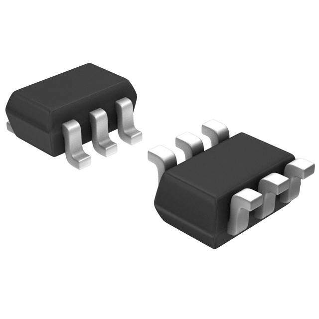
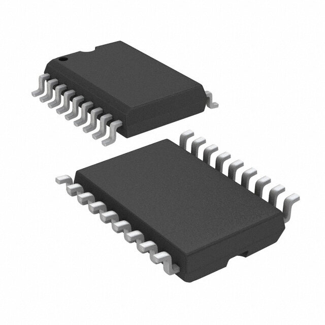
| 描述 | TVS USB 22OHM RES 5.25V SC70-6 |
| 产品分类 | |
| 品牌 | Semtech |
| 数据手册 | |
| 产品图片 |
|
| 产品型号 | STF203-22.TCT |
| rohs | 无铅 / 符合限制有害物质指令(RoHS)规范要求 |
| 产品系列 | - |
| 产品目录页面 | |
| 供应商器件封装 | SC-70-6 |
| 其它名称 | STF203-22TR |
| 功率(W) | 100mW |
| 包装 | 带卷 (TR) |
| 封装/外壳 | 6-TSSOP,SC-88,SOT-363 |
| 应用 | 通用 |
| 技术 | 混合技术 |
| 标准包装 | 3,000 |
| 电压-工作 | 5.25V |
| 电压-箝位 | - |
| 电路数 | 4 |


- 商务部:美国ITC正式对集成电路等产品启动337调查
- 曝三星4nm工艺存在良率问题 高通将骁龙8 Gen1或转产台积电
- 太阳诱电将投资9.5亿元在常州建新厂生产MLCC 预计2023年完工
- 英特尔发布欧洲新工厂建设计划 深化IDM 2.0 战略
- 台积电先进制程称霸业界 有大客户加持明年业绩稳了
- 达到5530亿美元!SIA预计今年全球半导体销售额将创下新高
- 英特尔拟将自动驾驶子公司Mobileye上市 估值或超500亿美元
- 三星加码芯片和SET,合并消费电子和移动部门,撤换高东真等 CEO
- 三星电子宣布重大人事变动 还合并消费电子和移动部门
- 海关总署:前11个月进口集成电路产品价值2.52万亿元 增长14.8%


PDF Datasheet 数据手册内容提取
STF203-15 THRU STF203-33 USB Upstream Port Filter and TVS For EMI Filtering and ESD Protection PPRROOTTEECCTTIIOONN PPRROODDUUCCTTSS Description Features The STF203 is a combination EMI filter and line (cid:139) Bidirectional EMI/RFI filtering and line termination termination device with integrated TVS diodes for use with integrated ESD protection on upstream USB ports. It is constructed using a (cid:139) ESD protection for USB power (V ) and data lines BUS proprietary technology that allows passive components (D+ and D-) to and TVS diodes to be integrated in the same package. IEC 61000-4-2 (ESD) ±15kV (air), ±8kV (contact) Each device will provide termination, filtering, and ESD IEC 61000-4-4 (EFT) 40A (5/50ns) protection for one upstream USB port. The STF203 is (cid:139) Filtering and termination for one USB port an easily implemented solution for meeting the (cid:139) Series resistors: 15Ω, 22Ω, and 33Ω requirements of revision 1.1 of the Universal Serial Bus (cid:139) Low TVS operating voltage (5.25V) specification. (cid:139) Low leakage current Line termination is achieved with series resistors on (cid:139) Small SC70-6L package both the D+ and D- USB lines. The value of series (cid:139) Solid-state technology resistance added to the output impedance of the USB Ω driver must be as close to possible to the 45 Mechanical Characteristics Ω characteristic impedance of the cable (90 balanced) (cid:139) EIAJ SC70-6L package to minimize transmission line reflections. They are Ω (cid:139) RoHS/WEEE Compliant available with resistor values of 15 (STF203-15), Ω Ω Ω (cid:139) Molding compound flammability rating: UL 94V-0 22 (STF203-22), and 33 (STF203-33). The 1.5k (cid:139) Marking : Marking Code pull-up resistor is required by the USB specification to identify the equipment as either a full-speed (cid:139) Packaging : Tape and Reel per EIA 481 (connected to D+ line) or low-speed (connected to D- Applications line) device. The 47pF capacitors are required to bypass high frequency energy to ground and to control (cid:139) USB Ports the edge rate of the USB signals. The TVS diodes (cid:139) Cellular Handsets provide ESD protection of both (D+ and D-) data lines (cid:139) PDAs and the voltage bus (V ). The TVS diodes on the (cid:139) Pagers BUS input/output pins provide suppression of ESD voltages (cid:139) Digital Cameras in excess of ±15kV (air discharge) and ±8kV (contact (cid:139) PC Peripherals discharge) per IEC 61000-4-2, level 4. The TVS diode (cid:139) MP3 Players on the V pin will suppress ESD discharges in excess BUS of 25kV per IEC 61000-4-2. Circuit Diagram Schematic and PIN Configuration 6 1 D In/Out D In/Out . 2 5 4 3 D In/Out D In/Out SC70-6L (Top View) Revision 03/22/2006 1 www.semtech.com
STF203-15 THRU STF203-33 PROTECTION PRODUCTS Absolute Maximum Rating Rating Symbol Value Units Steady-StatePower P 100 mW SS ESDAirDischargeperIEC61000-4-2 16 kV V ESDContact DischargeperIEC61000-4-2 ESD 10 Lead Soldering Temperature T 260(10sec.) °C L Operating Temperature T -40to+125 °C J StorageTemperature T -55to+150 °C STG Electrical Characteristics STF203-XX Parameter Symbol Conditions Minimum Typical Maximum Units TVSReverseStand-Off Voltage V 5.25 V RWM TVSReverseBreakdown Voltage V I =1mA 6 V BR t TVSReverseLeakageCurrent I V =5.25V, T=25°C 5 µA R RWM Between and data (D+, D-) pin and Ground TVSReverseLeakageCurrent I Each Line 1 µA R SeriesResistance(STF203-15) R Each Line 13.5 15 16.5 Ohms S SeriesResistance(STF203-22) R Each Line 20 22 24 Ohms S SeriesResistance(STF203-33) R Each Line 30 33 36 Ohms S Pull Up Resistance R 1.35 1.5 1.65 kOhms PU Capacitor C Each Line 47 pF Total Capacitance C Between Input or 60 pF TOT Output orGround V =0V, f =1MHz R 2006 Semtech Corp. 2 www.semtech.com
STF203-15 THRU STF203-33 PROTECTION PRODUCTS Typical Characteristics ESD Clamping (8kV Contact) ESD Clamping (15kV Air) Typical Insertion Loss Analog Crosstalk (D+ to D-) CH1 S21 LOG 3 dB / REF 0 dB CH1 S21 log MAG 20 dB/ REF 0 dB 1: -20.394 dB 800 MHz PRm 2: -15.035 dB 0 dB 1.8 GHz -3 dB 3: -14.781 dB 2.5 GHz -6 dB -9 dB -12 dB 3 -15 dB 2 -18 dB -21 dB 1 -24 dB 1 10 100 1 3 MHz MHz MHz GHz GHz START .030 000 MHz STOP 3 000.000 000 MHz START . 030 MHz STOP 3 000. 0000 00 MHz 2006 Semtech Corp. 3 www.semtech.com
STF203-15 THRU STF203-33 PROTECTION PRODUCTS Applications Information Figure 1 - Preferred Connection Diagram Device Connection (Full Speed Devices) The STF203 is designed to provide termination, EMI filtering and ESD protection for one USB port. The From Connector device is connected as follows: 1 STF203 6 11111..... Full-Speed Devices: For full-speed devices the 2 5 pull-up resistor is connected to the D+ line. Route the D+ line from the connector to pin 1 of the 3 4 STF203. Pin 6 is connected to the D+ line of the IC. Route the D- line from the connector to pin 3. Pin 4 is connected to the D- line of the IC. Pin 5 is connected to the voltage supply line (V ). Pin 2 is BUS connected to ground. Note that the input and Figure 2 - Preferred Connection Diagram output connections may be reversed if necessary (Low Speed Devices) (See Figure 3). From Connector 22222..... Low-Speed Devices::::: For low speed devices the 1 STF203 6 pull-up resistor is connected to the D- line. Route the D- line from the connector to pin 1 of the 2 5 STF203. Pin 6 is connected to the D- line of the IC. 3 4 Route the D+ line from the connector to pin 3. Pin 4 is connected to the D+ line of the IC. Pin 5 is connected to the voltage supply line (V ). Pin 2 is BUS connected to ground. Note that the input and output connections may be reversed if necessary Figure 3 - Alternate Connection Diagram (See Figure 4). (Full Speed Devices) USB Port Design Considerations From Connector The Universal Serial Bus (USB) specification requires 1 STF203 6 termination and filtering components for proper opera- 2 5 tion. In addition, an open USB socket is vulnerable to hazardous ESD discharges in excess of 15kV. These 3 4 discharges can occur on the data lines or the voltage bus. The STF203 is an easily implemented solution that is designed to meet the termination and EMI filter requirements of the USB specification revision 1.1. It also provides ESD protection to IEC 61000-4-2, Figure 4 - Alternate Connection Diagram level 4. (Low Speed Devices) USB line termination is achieved with series resistors From Connector on both the D+ and D- lines. These resistors preserve 1 STF203 6 signal integrity by matching the cable impedance to that of the differential driver. A 1.5kΩ pull-up resistor 2 5 is used to identify an upstream port on either the D+ 3 4 (full speed devices) or the D- (low speed devices) data line. Capacitors are used for EMI suppression. TVS diodes provide ESD protection of both (D+ and D-) data lines and the voltage bus (V ). The STF203 BUS integrates all of these components in a small SC-70 package. This integrated solution simplifies design and requires minimal board space. 2006 Semtech Corp. 4 www.semtech.com
STF203-15 THRU STF203-33 PROTECTION PRODUCTS Outline Drawing - SC70 6L A DIMENSIONS e1 D DIM INCHES MILLIMETERS MIN NOMMAX MIN NOMMAX N A - - .043 - - 1.10 A1 .000 - .004 0.00 - 0.10 2X E/2 SEE DETAIL A A2 .028 .035 .039 0.70 0.90 1.00 EI E SIDE VIEW b .006 - .012 0.15 - 0.30 c .003 - .009 0.08 - 0.22 D .075 .079 .083 1.90 2.00 2.10 ccc C 1 2 E1 .045 .049 .053 1.15 1.25 1.35 E .083 BSC 2.10 BSC 2X N/2 TIPS e H e .026 BSC 0.65 BSC e1 .051 1.30 BSC B L .010 .014 .018 0.26 0.36 0.46 GAGE c L1 (.017) (0.42) PLANE N 6 6 D 01 0° - 8° 0° - 8° 0.15 L aaa .004 0.10 aaa C 01 bbb .004 0.10 A2 A (L1) ccc .012 0.30 SEATING DETAIL A PLANE C A1 bxN bbb C A-B D NOTES: 1. CONTROLLING DIMENSIONS ARE IN MILLIMETERS (ANGLES IN DEGREES). 2. DATUMS - A - AND - B - TO BE DETERMINED AT DATUM PLANE-H- 3. DIMENSIONS "E1" AND "D" DO NOT INCLUDE MOLD FLASH, PROTRUSIONS OR GATE BURRS. 4. REFERENCE JEDEC STD MO-203, VARIATION AB. Land Pattern - SC70 6L X DDIIMMEENNSSIIOONNSS DDIIMM IINNCCHHEESS MMIILLLLIIMMEETTEERRSS CC (.073) (1.85) GG .039 1.00 C G Z PP .026 0.65 XX .016 0.40 Y YY .033 0.85 ZZ .106 2.70 P NOTES: 1. THIS LAND PATTERN IS FOR REFERENCE PURPOSES ONLY. CONSULT YOUR MANUFACTURING GROUP TO ENSURE YOUR COMPANY'S MANUFACTURING GUIDELINES ARE MET. 2006 Semtech Corp. 5 www.semtech.com
STF203-15 THRU STF203-33 PROTECTION PRODUCTS Marking Ordering Information Series Marking Qtyper Part Number Part Number Lead Finish ReelSize Resistor Code Reel STF203-15 15Ω 315 STF203-15.TC SnPb 3,000 7” STF203-22 22Ω 322 STF203-22.TC SnPb 3,000 7” STF203-33 33Ω 333 STF203-33.TC SnPb 3,000 7” STF203-15.TCT Pb free 3,000 7” 6 5 4 STF203-22.TCT Pb free 3,000 7” XXX STF203-33.TCT Pb free 3,000 7” Note: Pb free finish is matte tin 1 2 3 Note: XXX = Marking Code Contact Information Semtech Corporation Protection Products Division 200 Flynn Road, Camarillo, CA 93012 Phone: (805)498-2111 FAX (805)498-3804 2006 Semtech Corp. 6 www.semtech.com