ICGOO在线商城 > 分立半导体产品 > 晶体管 - FET,MOSFET - 单 > STF14NM50N
 Datasheet下载
- 型号: STF14NM50N
- 制造商: STMicroelectronics
- 库位|库存: xxxx|xxxx
- 要求:
| 数量阶梯 | 香港交货 | 国内含税 |
| +xxxx | $xxxx | ¥xxxx |
查看当月历史价格
查看今年历史价格
STF14NM50N产品简介:
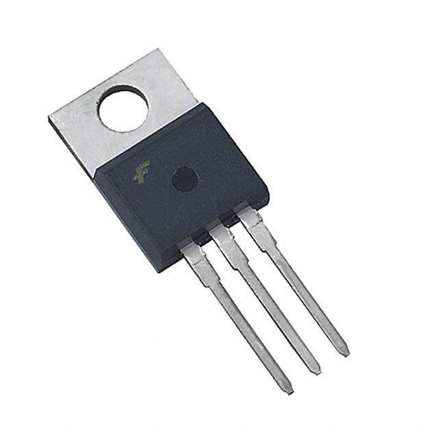
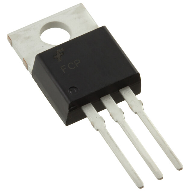
ICGOO电子元器件商城为您提供STF14NM50N由STMicroelectronics设计生产,在icgoo商城现货销售,并且可以通过原厂、代理商等渠道进行代购。 STF14NM50N价格参考。STMicroelectronicsSTF14NM50N封装/规格:晶体管 - FET,MOSFET - 单, 通孔 N 沟道 500V 12A(Tc) 25W(Tc) TO-220FP。您可以下载STF14NM50N参考资料、Datasheet数据手册功能说明书,资料中有STF14NM50N 详细功能的应用电路图电压和使用方法及教程。
| 参数 | 数值 |
| 产品目录 | |
| ChannelMode | Enhancement |
| 描述 | MOSFET N-CH 500V 12A TO220FPMOSFET N-Ch 500V 0.246 Ohm 12A Mdmesh 2 PWR MO |
| 产品分类 | FET - 单分离式半导体 |
| FET功能 | 标准 |
| FET类型 | MOSFET N 通道,金属氧化物 |
| Id-ContinuousDrainCurrent | 12 A |
| Id-连续漏极电流 | 12 A |
| 品牌 | STMicroelectronics |
| 产品手册 | |
| 产品图片 |
|
| rohs | 符合RoHS无铅 / 符合限制有害物质指令(RoHS)规范要求 |
| 产品系列 | 晶体管,MOSFET,STMicroelectronics STF14NM50NMDmesh™ II |
| 数据手册 | |
| 产品型号 | STF14NM50N |
| Pd-PowerDissipation | 25 W |
| Pd-功率耗散 | 25 W |
| Qg-GateCharge | 27 nC |
| Qg-栅极电荷 | 27 nC |
| RdsOn-Drain-SourceResistance | 320 mOhms |
| RdsOn-漏源导通电阻 | 320 mOhms |
| Vds-Drain-SourceBreakdownVoltage | 500 V |
| Vds-漏源极击穿电压 | 500 V |
| Vgs-Gate-SourceBreakdownVoltage | +/- 25 V |
| Vgs-栅源极击穿电压 | 25 V |
| 上升时间 | 16 ns |
| 下降时间 | 22 ns |
| 不同Id时的Vgs(th)(最大值) | 4V @ 100µA |
| 不同Vds时的输入电容(Ciss) | 816pF @ 50V |
| 不同Vgs时的栅极电荷(Qg) | 27nC @ 10V |
| 不同 Id、Vgs时的 RdsOn(最大值) | 320 毫欧 @ 6A,10V |
| 产品种类 | MOSFET |
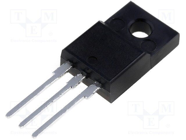
| 供应商器件封装 | TO-220FP |
| 其它名称 | 497-12569-5 |
| 其它有关文件 | http://www.st.com/web/catalog/sense_power/FM100/CL824/SC1167/PF248451?referrer=70071840 |
| 典型关闭延迟时间 | 42 ns |
| 功率-最大值 | 25W |
| 包装 | 管件 |
| 商标 | STMicroelectronics |
| 安装类型 | 通孔 |
| 安装风格 | Through Hole |
| 封装 | Tube |
| 封装/外壳 | TO-220-3 整包 |
| 封装/箱体 | TO-220FP-3 |
| 工厂包装数量 | 50 |
| 晶体管极性 | N-Channel |
| 最大工作温度 | + 150 C |
| 最小工作温度 | - 55 C |
| 标准包装 | 50 |
| 漏源极电压(Vdss) | 500V |
| 电流-连续漏极(Id)(25°C时) | 12A (Tc) |
| 系列 | STF14NM50N |
| 通道模式 | Enhancement |
| 配置 | Single |


- 商务部:美国ITC正式对集成电路等产品启动337调查
- 曝三星4nm工艺存在良率问题 高通将骁龙8 Gen1或转产台积电
- 太阳诱电将投资9.5亿元在常州建新厂生产MLCC 预计2023年完工
- 英特尔发布欧洲新工厂建设计划 深化IDM 2.0 战略
- 台积电先进制程称霸业界 有大客户加持明年业绩稳了
- 达到5530亿美元!SIA预计今年全球半导体销售额将创下新高
- 英特尔拟将自动驾驶子公司Mobileye上市 估值或超500亿美元
- 三星加码芯片和SET,合并消费电子和移动部门,撤换高东真等 CEO
- 三星电子宣布重大人事变动 还合并消费电子和移动部门
- 海关总署:前11个月进口集成电路产品价值2.52万亿元 增长14.8%


PDF Datasheet 数据手册内容提取
STF14NM50N, STI14NM50N, STP14NM50N Ω N-channel 500 V, 0.28 typ., 12 A MDmesh™ II Power MOSFETs in TO-220FP, I²PAK and TO-220 packages Datasheet - production data Features V @ R Order codes DS DS(on) I T max D Jmax 3 STF14NM50N 2 1 STI14NM50N 550 V 0.32 Ω 12 A TO-220FP TAB TAB STP14NM50N • 100% avalanche tested • Low input capacitance and gate charge I2PAK 23 TO-220 23 • Low gate input resistance 1 1 Applications Figure 1. Internal schematic diagram • Switching applications (cid:39)(cid:11)(cid:21)(cid:15)(cid:3)(cid:55)(cid:36)(cid:37)(cid:12) Description These devices are N-channel Power MOSFET developed using the second generation of (cid:42)(cid:11)(cid:20)(cid:12) MDmesh™ technology. This revolutionary Power MOSFET associates a vertical structure to the company’s strip layout to yield one of the world’s lowest on-resistance and gate charge. It is (cid:54)(cid:11)(cid:22)(cid:12) therefore suitable for the most demanding high efficiency converters. (cid:36)(cid:48)(cid:19)(cid:20)(cid:23)(cid:26)(cid:24)(cid:89)(cid:20) Table 1. Device summary Order codes Marking Package Packaging STF14NM50N TO-220FP STI14NM50N 14NM50N I2PAK Tube STP14NM50N TO-220 June 2014 DocID16832 Rev 7 1/18 This is information on a product in full production. www.st.com 18
Contents STF14NM50N, STI14NM50N, STP14NM50N Contents 1 Electrical ratings . . . . . . . . . . . . . . . . . . . . . . . . . . . . . . . . . . . . . . . . . . . . 3 2 Electrical characteristics . . . . . . . . . . . . . . . . . . . . . . . . . . . . . . . . . . . . . 4 2.1 Electrical characteristics (curves) . . . . . . . . . . . . . . . . . . . . . . . . . . . . 6 3 Test circuits . . . . . . . . . . . . . . . . . . . . . . . . . . . . . . . . . . . . . . . . . . . . . . 9 4 Package mechanical data . . . . . . . . . . . . . . . . . . . . . . . . . . . . . . . . . . . . 10 4.1 TO-220FP, STF14NM50N . . . . . . . . . . . . . . . . . . . . . . . . . . . . . . . . . . . . .11 4.2 I2PAK, STI14NM50N . . . . . . . . . . . . . . . . . . . . . . . . . . . . . . . . . . . . . . . . 13 4.3 TO-220, STP14NM50N . . . . . . . . . . . . . . . . . . . . . . . . . . . . . . . . . . . . . . 15 5 Revision history . . . . . . . . . . . . . . . . . . . . . . . . . . . . . . . . . . . . . . . . . . . 17 2/18 DocID16832 Rev 7
STF14NM50N, STI14NM50N, STP14NM50N Electrical ratings 1 Electrical ratings Table 2. Absolute maximum ratings Value Symbol Parameter Unit I²PAK, TO-220 TO-220FP V Drain-source voltage 500 V DS V Gate-source voltage ± 25 V GS I Drain current (continuous) at T = 25 °C 12 12 (1) A D C I Drain current (continuous) at T = 100 °C 8 8 (1) A D C I (2) Drain current (pulsed) 48 48 (1) A DM P Total dissipation at T = 25 °C 90 25 W TOT C dv/dt (3) Peak diode recovery voltage slope 15 V/ns Insulation withstand voltage (RMS) from all V three leads to external heat sink 2500 V ISO (t = 1 s; TC = 25 °C) T Storage temperature - 55 to 150 °C stg T Max. operating junction temperature 150 °C j 1. Limited by maximum junction temperature 2. Pulse width limited by safe operating area 3. I ≤ 12 A, di/dt ≤ 400 A/s,V peak ≤ V , V = 80% V SD DS (BR)DSS DD (BR)DSS Table 3. Thermal data Value Symbol Parameter Unit TO-220FP I²PAK TO-220 R Thermal resistance junction-case max 5 1.39 °C/W thj-case R Thermal resistance junction-ambient max 62.5 °C/W thj-amb Table 4. Avalanche data Symbol Parameter Value Unit Avalanche current, repetitive or not-repetitive I 4 A AR (pulse width limited by T max) j Single pulse avalanche energy E 172 mJ AS (starting T = 25°C, I = I , V = 50 V) j D AR DD DocID16832 Rev 7 3/18
Electrical characteristics STF14NM50N, STI14NM50N, STP14NM50N 2 Electrical characteristics (T = 25 °C unless otherwise specified) C Table 5. On /off states Symbol Parameter Test conditions Min. Typ. Max. Unit Drain-source V I = 1 mA, V = 0 500 V (BR)DSS breakdown voltage D GS Zero gate voltage V = 500 V 1 µA I DS DSS drain current (V = 0) V = 500 V, T =125 °C 100 µA GS DS C Gate-body leakage I V = ± 25 V ± 100 nA GSS current (V = 0) GS DS V Gate threshold voltage V = V , I = 250 µA 2 3 4 V GS(th) DS GS D Static drain-source R V = 10 V, I = 6 A 0.28 0.32 Ω DS(on) on-resistance GS D Table 6. Dynamic Symbol Parameter Test conditions Min. Typ. Max. Unit Input capacitance C 816 pF Ciss Output capacitance VDS = 50 V, f = 1 MHz, - 60 - pF Coss Reverse transfer VGS = 0 3 pF rss capacitance Equivalent output C (1) V = 0 to 50 V, V = 0 - 157 - pF oss eq. capacitance DS GS Intrinsic gate R f = 1 MHz open drain - 4.5 - Ω G resistance Q Total gate charge 27 nC g V =400 V, I =12 A, Q Gate-source charge DD D - 5 - nC gs V =10 V (see Figure16) GS Q Gate-drain charge 15 nC gd 1. C is defined as a constant equivalent capacitance giving the same charging time as C when V oss eq. oss DS increases from 0 to 80% V DS Table 7. Switching times Symbol Parameter Test conditions Min. Typ. Max. Unit t Turn-on delay time 12 ns d(on) V = 400 V, I = 12 A, t Rise time DD D 16 ns r RG =4.7 Ω, VGS = 10 V - - t Turn-off-delay time 42 ns d(off) (see Figure17) t Fall time 22 ns f 4/18 DocID16832 Rev 7
STF14NM50N, STI14NM50N, STP14NM50N Electrical characteristics Table 8. Source drain diode Symbol Parameter Test conditions Min. Typ. Max. Unit I Source-drain current 12 A SD - I (1) Source-drain current (pulsed) 48 A SDM V (2) Forward on voltage I = 12 A, V = 0 - 1.6 V SD SD GS trr Reverse recovery time ISD = 12 A, di/dt = 100 A/µs, 252 ns Q Reverse recovery charge V = 60 V - 2.8 µC rr DD I Reverse recovery current (see Figure20) 22 A RRM trr Reverse recovery time ISD = 12 A, di/dt = 100 A/µs, 300 ns Q Reverse recovery charge V = 60 V, T = 150 °C - 3.3 µC rr DD J I Reverse recovery current (see Figure20) 22.2 A RRM 1. Pulse width limited by safe operating area. 2. Pulsed: pulse duration = 300 µs, duty cycle 1.5% DocID16832 Rev 7 5/18
Electrical characteristics STF14NM50N, STI14NM50N, STP14NM50N 2.1 Electrical characteristics (curves) Figure 2. Safe operating area for I²PAK, TO-220 Figure 3. Thermal impedance for I²PAK, TO-220 ID AM07199v1 (A) 10 Operatimiotne id n btyh ism aarx eRa iDsS(on) 11000µµss 1 Li 1ms 10ms Tj=150°C Tc=25°C Single pulse 0.1 0.1 1 10 100 VDS(V) Figure 4. Safe operating area for TO-220FP Figure 5. Thermal impedance for TO-220FP ID AM07201v1 (A) 101 OpeLiratmiitoen di nb yt hims aax reRa DiSs(on) 11000µµss 1ms 10ms 0.1 Tj=150°C Tc=25°C Single pulse 0.01 0.1 1 10 100 VDS(V) Figure 6. Output characteristics Figure 7. Transfer characteristics AM07202v1 AM07203v1 ID ID (A) (A) VGS=10V 25 25 VDS=18V 20 20 6V 15 15 10 10 5V 5 5 0 0 0 5 10 15 20 VDS(V) 0 2 4 6 8 10VGS(V) 6/18 DocID16832 Rev 7
STF14NM50N, STI14NM50N, STP14NM50N Electrical characteristics Figure 8. Normalized V vs temperature Figure 9. Static drain-source on-resistance (BR)DSS V(BR)DSS AM09028v1 RDS(on) AM07205v1 (norm) ID=1mA (Ohm) 1.10 0.300 VGS=10V 1.08 0.295 1.06 0.290 1.04 1.02 0.285 1.00 0.280 0.98 0.275 0.96 0.270 0.94 0.92 0.265 -50 -25 0 25 50 75 100 TJ(°C) 0 2 4 6 8 10 12 ID(A) Figure 10. Capacitance variations Figure 11. Gate charge vs gate-source voltage C AM07206v1 VGS AMV0D7S204v1 (pF) (V) (V) 400 12 VDD=400V VDS ID=12A 350 1000 Ciss 10 300 8 250 100 200 6 Coss 150 4 10 100 Crss 2 50 1 0 0 0.1 1 10 100 VDS(V) 0 5 10 15 20 25 30 Qg(nC) Figure 12. Normalized gate threshold voltage vs Figure 13. Normalized on-resistance vs temperature temperature VGS(th) AM07208v1 RDS(on) AM07209v1 (norm) ID=250µA (norm) 1.10 2.1 ID=6A 1.00 1.7 VGS=10 V 0.90 1.3 0.80 0.9 0.70 0.5 -50 -25 0 25 50 75 100 TJ(°C) -50 -25 0 25 50 75 100 TJ(°C) DocID16832 Rev 7 7/18
Electrical characteristics STF14NM50N, STI14NM50N, STP14NM50N Figure 14. Source-drain diode forward characteristics VSD AM15616v1 (V) 1.4 TJ= -50 °C 1.2 1 TJ= 25 °C 0.8 TJ= 150 °C 0.6 0.4 0.2 0 0 1 2 3 4 5 6 7 8 9 10 11 ISD(A) 8/18 DocID16832 Rev 7
STF14NM50N, STI14NM50N, STP14NM50N Test circuits 3 Test circuits Figure 15. Switching times test circuit for Figure 16. Gate charge test circuit resistive load VDD 12V 47kΩ 1kΩ 100nF RL 2μ20F0 3μ.F3 VDD IG=CONST VD Vi=20V=VGMAX 100Ω D.U.T. VGS 2200 RG D.U.T. μF 2.7kΩ VG PW 47kΩ 1kΩ PW AM01468v1 AM01469v1 Figure 17. Test circuit for inductive load Figure 18. Unclamped inductive load test circuit switching and diode recovery times L A A A D FAST L=100μH VD G D.U.T. DIODE 2200 3.3 μF μF VDD S B 3.3 1000 B B μF μF 25Ω D VDD ID G RG S Vi D.U.T. Pw AM01470v1 AM01471v1 Figure 19. Unclamped inductive waveform Figure 20. Switching time waveform V(BR)DSS ton toff VD tdon tr tdoff tf 90% 90% IDM 10% ID 0 10% VDS VDD VDD 90% VGS AM01472v1 0 10% AM01473v1 DocID16832 Rev 7 9/18
Package mechanical data STF14NM50N, STI14NM50N, STP14NM50N 4 Package mechanical data In order to meet environmental requirements, ST offers these devices in different grades of ECOPACK® packages, depending on their level of environmental compliance. ECOPACK® specifications, grade definitions and product status are available at: www.st.com. ECOPACK® is an ST trademark. 10/18 DocID16832 Rev 7
STF14NM50N, STI14NM50N, STP14NM50N Package mechanical data 4.1 TO-220FP, STF14NM50N Figure 21. TO-220FP drawing 7012510_Rev_K_B DocID16832 Rev 7 11/18
Package mechanical data STF14NM50N, STI14NM50N, STP14NM50N Table 9. TO-220FP mechanical data mm Dim. Min. Typ. Max. A 4.4 4.6 B 2.5 2.7 D 2.5 2.75 E 0.45 0.7 F 0.75 1 F1 1.15 1.70 F2 1.15 1.70 G 4.95 5.2 G1 2.4 2.7 H 10 10.4 L2 16 L3 28.6 30.6 L4 9.8 10.6 L5 2.9 3.6 L6 15.9 16.4 L7 9 9.3 Dia 3 3.2 12/18 DocID16832 Rev 7
STF14NM50N, STI14NM50N, STP14NM50N Package mechanical data 2 4.2 I PAK, STI14NM50N Figure 22. I²PAK (TO-262) drawing 0004982_Rev_H DocID16832 Rev 7 13/18
Package mechanical data STF14NM50N, STI14NM50N, STP14NM50N Table 10. I²PAK (TO-262) mechanical data mm. DIM. min. typ max. A 4.40 4.60 A1 2.40 2.72 b 0.61 0.88 b1 1.14 1.70 c 0.49 0.70 c2 1.23 1.32 D 8.95 9.35 e 2.40 2.70 e1 4.95 5.15 E 10 10.40 L 13 14 L1 3.50 3.93 L2 1.27 1.40 14/18 DocID16832 Rev 7
STF14NM50N, STI14NM50N, STP14NM50N Package mechanical data 4.3 TO-220, STP14NM50N Figure 23. TO-220 type A drawing (cid:19)(cid:19)(cid:20)(cid:24)(cid:28)(cid:27)(cid:27)(cid:66)(cid:87)(cid:92)(cid:83)(cid:72)(cid:36)(cid:66)(cid:53)(cid:72)(cid:89)(cid:66)(cid:55) DocID16832 Rev 7 15/18
Package mechanical data STF14NM50N, STI14NM50N, STP14NM50N Table 11. TO-220 type A mechanical data mm Dim. Min. Typ. Max. A 4.40 4.60 b 0.61 0.88 b1 1.14 1.70 c 0.48 0.70 D 15.25 15.75 D1 1.27 E 10 10.40 e 2.40 2.70 e1 4.95 5.15 F 1.23 1.32 H1 6.20 6.60 J1 2.40 2.72 L 13 14 L1 3.50 3.93 L20 16.40 L30 28.90 ∅ P 3.75 3.85 Q 2.65 2.95 16/18 DocID16832 Rev 7
STF14NM50N, STI14NM50N, STP14NM50N Revision history 5 Revision history Table 12. Document revision history Date Revision Changes 26-Nov-2009 1 First release. 02-Dec-2009 2 Inserted table footnote Table3: Thermal data. 22-Jul-2010 3 Document status promoted from preliminary data to datasheet. 06-Apr-2011 4 Updated E in Table2. AS Updated Figure1: Internal schematic diagram,Table1: Device summary, Table2: Absolute maximum ratings, Table3: Thermal 30-Oct-2012 5 data, Table5: On /off states. Updated Section4: Package mechanical data. Minor text changes. – Minor text changes – Added: Figure14 07-Feb-2013 6 – Updated: Section4: Package mechanical data only for DPAK package – The root part numbers STB14NM50N and STD14NM50N have been moved to a separate datasheet 05-Jun-2014 7 – Updated Coss eq. in Table6: Dynamic – Updated: Section4.3: TO-220, STP14NM50N – Minor text changes DocID16832 Rev 7 17/18
STF14NM50N, STI14NM50N, STP14NM50N Please Read Carefully: Information in this document is provided solely in connection with ST products. STMicroelectronics NV and its subsidiaries (“ST”) reserve the right to make changes, corrections, modifications or improvements, to this document, and the products and services described herein at any time, without notice. All ST products are sold pursuant to ST’s terms and conditions of sale. Purchasers are solely responsible for the choice, selection and use of the ST products and services described herein, and ST assumes no liability whatsoever relating to the choice, selection or use of the ST products and services described herein. No license, express or implied, by estoppel or otherwise, to any intellectual property rights is granted under this document. If any part of this document refers to any third party products or services it shall not be deemed a license grant by ST for the use of such third party products or services, or any intellectual property contained therein or considered as a warranty covering the use in any manner whatsoever of such third party products or services or any intellectual property contained therein. UNLESS OTHERWISE SET FORTH IN ST’S TERMS AND CONDITIONS OF SALE ST DISCLAIMS ANY EXPRESS OR IMPLIED WARRANTY WITH RESPECT TO THE USE AND/OR SALE OF ST PRODUCTS INCLUDING WITHOUT LIMITATION IMPLIED WARRANTIES OF MERCHANTABILITY, FITNESS FOR A PARTICULAR PURPOSE (AND THEIR EQUIVALENTS UNDER THE LAWS OF ANY JURISDICTION), OR INFRINGEMENT OF ANY PATENT, COPYRIGHT OR OTHER INTELLECTUAL PROPERTY RIGHT. ST PRODUCTS ARE NOT DESIGNED OR AUTHORIZED FOR USE IN: (A) SAFETY CRITICAL APPLICATIONS SUCH AS LIFE SUPPORTING, ACTIVE IMPLANTED DEVICES OR SYSTEMS WITH PRODUCT FUNCTIONAL SAFETY REQUIREMENTS; (B) AERONAUTIC APPLICATIONS; (C) AUTOMOTIVE APPLICATIONS OR ENVIRONMENTS, AND/OR (D) AEROSPACE APPLICATIONS OR ENVIRONMENTS. WHERE ST PRODUCTS ARE NOT DESIGNED FOR SUCH USE, THE PURCHASER SHALL USE PRODUCTS AT PURCHASER’S SOLE RISK, EVEN IF ST HAS BEEN INFORMED IN WRITING OF SUCH USAGE, UNLESS A PRODUCT IS EXPRESSLY DESIGNATED BY ST AS BEING INTENDED FOR “AUTOMOTIVE, AUTOMOTIVE SAFETY OR MEDICAL” INDUSTRY DOMAINS ACCORDING TO ST PRODUCT DESIGN SPECIFICATIONS. PRODUCTS FORMALLY ESCC, QML OR JAN QUALIFIED ARE DEEMED SUITABLE FOR USE IN AEROSPACE BY THE CORRESPONDING GOVERNMENTAL AGENCY. Resale of ST products with provisions different from the statements and/or technical features set forth in this document shall immediately void any warranty granted by ST for the ST product or service described herein and shall not create or extend in any manner whatsoever, any liability of ST. ST and the ST logo are trademarks or registered trademarks of ST in various countries. Information in this document supersedes and replaces all information previously supplied. The ST logo is a registered trademark of STMicroelectronics. All other names are the property of their respective owners. © 2014 STMicroelectronics - All rights reserved STMicroelectronics group of companies Australia - Belgium - Brazil - Canada - China - Czech Republic - Finland - France - Germany - Hong Kong - India - Israel - Italy - Japan - Malaysia - Malta - Morocco - Philippines - Singapore - Spain - Sweden - Switzerland - United Kingdom - United States of America www.st.com 18/18 DocID16832 Rev 7
Mouser Electronics Authorized Distributor Click to View Pricing, Inventory, Delivery & Lifecycle Information: S TMicroelectronics: STP14NM50N STF14NM50N STI14NM50N