ICGOO在线商城 > 集成电路(IC) > 嵌入式 - 微控制器 > ST72F321BJ9T6
 Datasheet下载
- 型号: ST72F321BJ9T6
- 制造商: STMicroelectronics
- 库位|库存: xxxx|xxxx
- 要求:
| 数量阶梯 | 香港交货 | 国内含税 |
| +xxxx | $xxxx | ¥xxxx |
查看当月历史价格
查看今年历史价格
ST72F321BJ9T6产品简介:
ICGOO电子元器件商城为您提供ST72F321BJ9T6由STMicroelectronics设计生产,在icgoo商城现货销售,并且可以通过原厂、代理商等渠道进行代购。 ST72F321BJ9T6价格参考。STMicroelectronicsST72F321BJ9T6封装/规格:嵌入式 - 微控制器, ST7 微控制器 IC ST7 8-位 8MHz 60KB(60K x 8) 闪存 。您可以下载ST72F321BJ9T6参考资料、Datasheet数据手册功能说明书,资料中有ST72F321BJ9T6 详细功能的应用电路图电压和使用方法及教程。
| 参数 | 数值 |
| 产品目录 | 集成电路 (IC) |
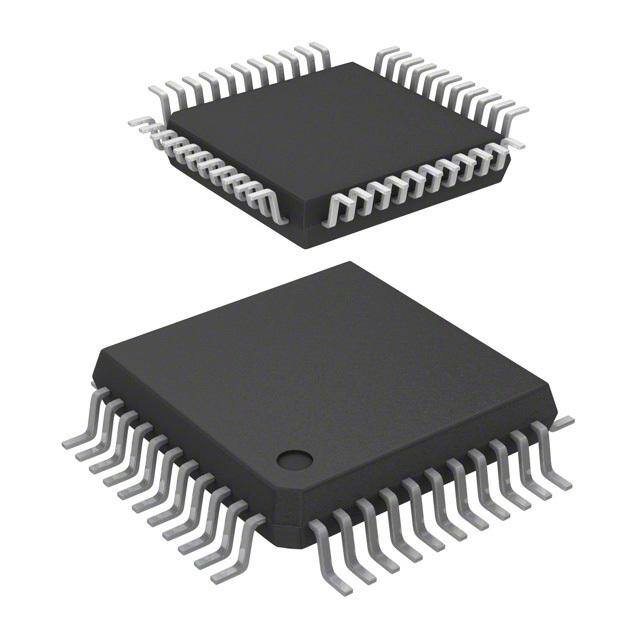
| 描述 | MCU 8BIT 60KB FLASH/ROM 44-LQFP |
| EEPROM容量 | - |
| 产品分类 | |
| I/O数 | 32 |
| 品牌 | STMicroelectronics |
| 数据手册 | |
| 产品图片 |
|
| 产品型号 | ST72F321BJ9T6 |
| RAM容量 | 2K x 8 |
| rohs | 无铅 / 符合限制有害物质指令(RoHS)规范要求 |
| 产品系列 | ST7 |
| 供应商器件封装 | * |
| 其它名称 | 497-5585 |
| 包装 | 托盘 |
| 外设 | LVD,POR,PWM,WDT |
| 封装/外壳 | 44-LQFP |
| 工作温度 | -40°C ~ 85°C |
| 振荡器类型 | 内部 |
| 数据转换器 | A/D 16x10b |
| 标准包装 | 160 |
| 核心处理器 | ST7 |
| 核心尺寸 | 8-位 |
| 特色产品 | http://www.digikey.com/product-highlights/cn/zh/segger-microcontroller-systems-flasher-tools/3226 |
| 电压-电源(Vcc/Vdd) | 3.8 V ~ 5.5 V |
| 程序存储器类型 | 闪存 |
| 程序存储容量 | 60KB(60K x 8) |
| 连接性 | I²C, SCI, SPI |
| 速度 | 8MHz |
| 配用 | /product-detail/zh/STX-RLINK/497-5046-ND/1013435 |


PDF Datasheet 数据手册内容提取
ST72321BRx, ST72321BARx ST72321BJx, ST72321BKx 64/44-pin 8-bit MCU with 32 to 60K Flash/ROM, ADC, 2 five timers, SPI, SCI, I C interface Features ■ Memories – 32K to 60K dual voltage High Density Flash (HDFlash) or ROM with read-out protection capability. In-Application Programming and In-Circuit Programming for HDFlash devices – 1K to 2K RAM LQFP64 LQFP32 14 x 14 7 x 7 – HDFlash endurance: 100 cycles, data reten- tion: 40 years at 85°C ■ Clock, Reset And Supply Management – Enhanced low voltage supervisor (LVD) for main supply and auxiliary voltage detector (AVD) with interrupt capability – Clock sources: crystal/ceramic resonator os- LQFP64 LQFP44 cillators, internal RC oscillator and bypass for 10 x 10 10 x 10 external clock – PLL for 2x frequency multiplication – 8-bit PWM Auto-reload timer with: 2 input cap- – Four Power Saving Modes: Halt, Active-Halt, tures, 4 PWM outputs, output compare and Wait and Slow time base interrupt, external clock with event ■ Interrupt Management detector – Nested interrupt controller ■ 3 Communications Interfaces – 14 interrupt vectors plus TRAP and RESET – SPI synchronous serial interface – Top Level Interrupt (TLI) pin on 64-pin devices – SCI asynchronous serial interface – 15/9 external interrupt lines (on 4 vectors) – I2C multimaster interface ■ Up to 48 I/O Ports ■ 1 Analog peripheral (low current coupling) – 48/32/24 multifunctional bidirectional I/O lines – 10-bit ADC with up to 16 robust input ports – 34/22/17 alternate function lines ■ Instruction Set – 16/12/10 high sink outputs – 8-bit Data Manipulation ■ 5 Timers – 63 Basic Instructions – Main Clock Controller with: Real time base, – 17 main Addressing Modes Beep and Clock-out capabilities – 8 x 8 Unsigned Multiply Instruction – Configurable watchdog timer ■ Development Tools – Two 16-bit timers with: 2 input captures, 2 out- – Full hardware/software development package put compares, external clock input on one tim- er, PWM and pulse generator modes – In-Circuit Testing capability Table 1. Device Summary ST72321BAR9/ ST72321BR9/ ST72321BAR7/ ST72321BR7/ ST72321BAR6/ ST72321BR6/ Features ST72321BJ9 ST72321BJ7 ST72321BJ6/ST72321BK6 Program memory - FLASH/ROM 60K FLASH/ROM 48K FLASH/ROM 32K bytes RAM (stack) - bytes 2048 (256) 1536 (256) 1024 (256) Operating Voltage 3.8V to 5.5V Temp. Range up to -40°C to +125°C Package LQFP64 10x10 (AR),LQFP64 14x14 (R), LQFP44 10x10 (J), LQFP32 7x7 (K) October 2008 Rev 5 1/187 1
Table of Contents 1 DESCRIPTION . . . . . . . . . . . . . . . . . . . . . . . . . . . . . . . . . . . . . . . . . . . . . . . . . . . . . . . . . . . . . . . 7 2 PIN DESCRIPTION . . . . . . . . . . . . . . . . . . . . . . . . . . . . . . . . . . . . . . . . . . . . . . . . . . . . . . . . . . . . 8 3 REGISTER & MEMORY MAP . . . . . . . . . . . . . . . . . . . . . . . . . . . . . . . . . . . . . . . . . . . . . . . . . . . 14 4 FLASH PROGRAM MEMORY . . . . . . . . . . . . . . . . . . . . . . . . . . . . . . . . . . . . . . . . . . . . . . . . . . 18 4.1 INTRODUCTION . . . . . . . . . . . . . . . . . . . . . . . . . . . . . . . . . . . . . . . . . . . . . . . . . . . . . . . . 18 4.2 MAIN FEATURES . . . . . . . . . . . . . . . . . . . . . . . . . . . . . . . . . . . . . . . . . . . . . . . . . . . . . . . 18 4.3 STRUCTURE . . . . . . . . . . . . . . . . . . . . . . . . . . . . . . . . . . . . . . . . . . . . . . . . . . . . . . . . . . . 18 4.3.1 Read-out Protection . . . . . . . . . . . . . . . . . . . . . . . . . . . . . . . . . . . . . . . . . . . . . . . . 18 4.4 ICC INTERFACE . . . . . . . . . . . . . . . . . . . . . . . . . . . . . . . . . . . . . . . . . . . . . . . . . . . . . . . . 19 4.5 ICP (IN-CIRCUIT PROGRAMMING) . . . . . . . . . . . . . . . . . . . . . . . . . . . . . . . . . . . . . . . . . 20 4.6 IAP (IN-APPLICATION PROGRAMMING) . . . . . . . . . . . . . . . . . . . . . . . . . . . . . . . . . . . . . 20 4.7 RELATED DOCUMENTATION . . . . . . . . . . . . . . . . . . . . . . . . . . . . . . . . . . . . . . . . . . . . . 20 4.7.1 Register Description . . . . . . . . . . . . . . . . . . . . . . . . . . . . . . . . . . . . . . . . . . . . . . . 20 5 CENTRAL PROCESSING UNIT . . . . . . . . . . . . . . . . . . . . . . . . . . . . . . . . . . . . . . . . . . . . . . . . . 21 5.1 INTRODUCTION . . . . . . . . . . . . . . . . . . . . . . . . . . . . . . . . . . . . . . . . . . . . . . . . . . . . . . . . 21 5.2 MAIN FEATURES . . . . . . . . . . . . . . . . . . . . . . . . . . . . . . . . . . . . . . . . . . . . . . . . . . . . . . . 21 5.3 CPU REGISTERS . . . . . . . . . . . . . . . . . . . . . . . . . . . . . . . . . . . . . . . . . . . . . . . . . . . . . . . 21 6 SUPPLY, RESET AND CLOCK MANAGEMENT . . . . . . . . . . . . . . . . . . . . . . . . . . . . . . . . . . . . 24 6.1 PHASE LOCKED LOOP . . . . . . . . . . . . . . . . . . . . . . . . . . . . . . . . . . . . . . . . . . . . . . . . . . 24 6.2 MULTI-OSCILLATOR (MO) . . . . . . . . . . . . . . . . . . . . . . . . . . . . . . . . . . . . . . . . . . . . . . . . 25 6.3 RESET SEQUENCE MANAGER (RSM) . . . . . . . . . . . . . . . . . . . . . . . . . . . . . . . . . . . . . . 26 6.3.1 Introduction . . . . . . . . . . . . . . . . . . . . . . . . . . . . . . . . . . . . . . . . . . . . . . . . . . . . . . 26 6.3.2 Asynchronous External RESET pin . . . . . . . . . . . . . . . . . . . . . . . . . . . . . . . . . . . . 26 6.3.3 External Power-On RESET . . . . . . . . . . . . . . . . . . . . . . . . . . . . . . . . . . . . . . . . . . 27 6.3.4 Internal Low Voltage Detector (LVD) RESET . . . . . . . . . . . . . . . . . . . . . . . . . . . . 27 6.3.5 Internal Watchdog RESET . . . . . . . . . . . . . . . . . . . . . . . . . . . . . . . . . . . . . . . . . . 27 6.4 SYSTEM INTEGRITY MANAGEMENT (SI) . . . . . . . . . . . . . . . . . . . . . . . . . . . . . . . . . . . . 28 6.4.1 Low Voltage Detector (LVD) . . . . . . . . . . . . . . . . . . . . . . . . . . . . . . . . . . . . . . . . . 28 6.4.2 Auxiliary Voltage Detector (AVD) . . . . . . . . . . . . . . . . . . . . . . . . . . . . . . . . . . . . . 29 6.4.3 Low Power Modes . . . . . . . . . . . . . . . . . . . . . . . . . . . . . . . . . . . . . . . . . . . . . . . . 30 6.4.4 Register Description . . . . . . . . . . . . . . . . . . . . . . . . . . . . . . . . . . . . . . . . . . . . . . . 31 7 INTERRUPTS . . . . . . . . . . . . . . . . . . . . . . . . . . . . . . . . . . . . . . . . . . . . . . . . . . . . . . . . . . . . . . . 32 7.1 INTRODUCTION . . . . . . . . . . . . . . . . . . . . . . . . . . . . . . . . . . . . . . . . . . . . . . . . . . . . . . . . 32 7.2 MASKING AND PROCESSING FLOW . . . . . . . . . . . . . . . . . . . . . . . . . . . . . . . . . . . . . . . 32 7.3 INTERRUPTS AND LOW POWER MODES . . . . . . . . . . . . . . . . . . . . . . . . . . . . . . . . . . . 34 7.4 CONCURRENT & NESTED MANAGEMENT . . . . . . . . . . . . . . . . . . . . . . . . . . . . . . . . . . 34 7.5 INTERRUPT REGISTER DESCRIPTION . . . . . . . . . . . . . . . . . . . . . . . . . . . . . . . . . . . . . 35 7.6 EXTERNAL INTERRUPTS . . . . . . . . . . . . . . . . . . . . . . . . . . . . . . . . . . . . . . . . . . . . . . . . 37 7.6.1 I/O Port Interrupt Sensitivity . . . . . . . . . . . . . . . . . . . . . . . . . . . . . . . . . . . . . . . . . . 37 7.7 EXTERNAL INTERRUPT CONTROL REGISTER (EICR) . . . . . . . . . . . . . . . . . . . . . . . . . 39 8 POWER SAVING MODES . . . . . . . . . . . . . . . . . . . . . . . . . . . . . . . . . . . . . . . . . . . . . . . . . . . . . 41 8.1 INTRODUCTION . . . . . . . . . . . . . . . . . . . . . . . . . . . . . . . . . . . . . . . . . . . . . . . . . . . . . . . . 41 187 8.2 SLOW MODE . . . . . . . . . . . . . . . . . . . . . . . . . . . . . . . . . . . . . . . . . . . . . . . . . . . . . . . . . . . 41 8.3 WAIT MODE . . . . . . . . . . . . . . . . . . . . . . . . . . . . . . . . . . . . . . . . . . . . . . . . . . . . . . . . . . . 42 2/187 1
Table of Contents 8.4 ACTIVE-HALT AND HALT MODES . . . . . . . . . . . . . . . . . . . . . . . . . . . . . . . . . . . . . . . . . . 43 8.4.1 ACTIVE-HALT MODE . . . . . . . . . . . . . . . . . . . . . . . . . . . . . . . . . . . . . . . . . . . . . . 43 8.4.2 HALT MODE . . . . . . . . . . . . . . . . . . . . . . . . . . . . . . . . . . . . . . . . . . . . . . . . . . . . . 44 9 I/O PORTS . . . . . . . . . . . . . . . . . . . . . . . . . . . . . . . . . . . . . . . . . . . . . . . . . . . . . . . . . . . . . . . . . . 46 9.1 INTRODUCTION . . . . . . . . . . . . . . . . . . . . . . . . . . . . . . . . . . . . . . . . . . . . . . . . . . . . . . . . 46 9.2 FUNCTIONAL DESCRIPTION . . . . . . . . . . . . . . . . . . . . . . . . . . . . . . . . . . . . . . . . . . . . . . 46 9.2.1 Input Modes . . . . . . . . . . . . . . . . . . . . . . . . . . . . . . . . . . . . . . . . . . . . . . . . . . . . . . 46 9.2.2 Output Modes . . . . . . . . . . . . . . . . . . . . . . . . . . . . . . . . . . . . . . . . . . . . . . . . . . . . 46 9.2.3 Alternate Functions . . . . . . . . . . . . . . . . . . . . . . . . . . . . . . . . . . . . . . . . . . . . . . . . 46 9.3 I/O PORT IMPLEMENTATION . . . . . . . . . . . . . . . . . . . . . . . . . . . . . . . . . . . . . . . . . . . . . . 49 9.4 LOW POWER MODES . . . . . . . . . . . . . . . . . . . . . . . . . . . . . . . . . . . . . . . . . . . . . . . . . . . 49 9.5 INTERRUPTS . . . . . . . . . . . . . . . . . . . . . . . . . . . . . . . . . . . . . . . . . . . . . . . . . . . . . . . . . . 49 9.5.1 I/O Port Implementation . . . . . . . . . . . . . . . . . . . . . . . . . . . . . . . . . . . . . . . . . . . . . 50 10 ON-CHIP PERIPHERALS . . . . . . . . . . . . . . . . . . . . . . . . . . . . . . . . . . . . . . . . . . . . . . . . . . . . . 52 10.1WATCHDOG TIMER (WDG) . . . . . . . . . . . . . . . . . . . . . . . . . . . . . . . . . . . . . . . . . . . . . . . 52 10.1.1 Introduction . . . . . . . . . . . . . . . . . . . . . . . . . . . . . . . . . . . . . . . . . . . . . . . . . . . . . . 52 10.1.2 Main Features . . . . . . . . . . . . . . . . . . . . . . . . . . . . . . . . . . . . . . . . . . . . . . . . . . . . 52 10.1.3 Functional Description . . . . . . . . . . . . . . . . . . . . . . . . . . . . . . . . . . . . . . . . . . . . . . 52 10.1.4 How to Program the Watchdog Timeout . . . . . . . . . . . . . . . . . . . . . . . . . . . . . . . . 53 10.1.5 Low Power Modes . . . . . . . . . . . . . . . . . . . . . . . . . . . . . . . . . . . . . . . . . . . . . . . . . 55 10.1.6 Hardware Watchdog Option . . . . . . . . . . . . . . . . . . . . . . . . . . . . . . . . . . . . . . . . . 55 10.1.7 Using Halt Mode with the WDG (WDGHALT option) . . . . . . . . . . . . . . . . . . . . . . . 55 10.1.8 Interrupts . . . . . . . . . . . . . . . . . . . . . . . . . . . . . . . . . . . . . . . . . . . . . . . . . . . . . . . . 55 10.1.9 Register Description . . . . . . . . . . . . . . . . . . . . . . . . . . . . . . . . . . . . . . . . . . . . . . . 55 10.2MAIN CLOCK CONTROLLER WITH REAL TIME CLOCK AND BEEPER (MCC/RTC) . . 57 10.2.1 Programmable CPU Clock Prescaler . . . . . . . . . . . . . . . . . . . . . . . . . . . . . . . . . . 57 10.2.2 Clock-out Capability . . . . . . . . . . . . . . . . . . . . . . . . . . . . . . . . . . . . . . . . . . . . . . . . 57 10.2.3 Real Time Clock Timer (RTC) . . . . . . . . . . . . . . . . . . . . . . . . . . . . . . . . . . . . . . . . 57 10.2.4 Beeper . . . . . . . . . . . . . . . . . . . . . . . . . . . . . . . . . . . . . . . . . . . . . . . . . . . . . . . . . . 57 10.2.5 Low Power Modes . . . . . . . . . . . . . . . . . . . . . . . . . . . . . . . . . . . . . . . . . . . . . . . . 58 10.2.6 Interrupts . . . . . . . . . . . . . . . . . . . . . . . . . . . . . . . . . . . . . . . . . . . . . . . . . . . . . . . . 58 10.2.7 Register Description . . . . . . . . . . . . . . . . . . . . . . . . . . . . . . . . . . . . . . . . . . . . . . . 58 10.3PWM AUTO-RELOAD TIMER (ART) . . . . . . . . . . . . . . . . . . . . . . . . . . . . . . . . . . . . . . . . . 60 10.3.1 Introduction . . . . . . . . . . . . . . . . . . . . . . . . . . . . . . . . . . . . . . . . . . . . . . . . . . . . . . 60 10.3.2 Functional Description . . . . . . . . . . . . . . . . . . . . . . . . . . . . . . . . . . . . . . . . . . . . . . 61 10.3.3 Register Description . . . . . . . . . . . . . . . . . . . . . . . . . . . . . . . . . . . . . . . . . . . . . . . 65 10.416-BIT TIMER . . . . . . . . . . . . . . . . . . . . . . . . . . . . . . . . . . . . . . . . . . . . . . . . . . . . . . . . . . 69 10.4.1 Introduction . . . . . . . . . . . . . . . . . . . . . . . . . . . . . . . . . . . . . . . . . . . . . . . . . . . . . . 69 10.4.2 Main Features . . . . . . . . . . . . . . . . . . . . . . . . . . . . . . . . . . . . . . . . . . . . . . . . . . . . 69 10.4.3 Functional Description . . . . . . . . . . . . . . . . . . . . . . . . . . . . . . . . . . . . . . . . . . . . . . 69 10.4.4 Low Power Modes . . . . . . . . . . . . . . . . . . . . . . . . . . . . . . . . . . . . . . . . . . . . . . . . 81 10.4.5 Interrupts . . . . . . . . . . . . . . . . . . . . . . . . . . . . . . . . . . . . . . . . . . . . . . . . . . . . . . . 81 10.4.6 Summary of Timer Modes . . . . . . . . . . . . . . . . . . . . . . . . . . . . . . . . . . . . . . . . . . 81 10.4.7 Register Description . . . . . . . . . . . . . . . . . . . . . . . . . . . . . . . . . . . . . . . . . . . . . . . 82 10.5SERIAL PERIPHERAL INTERFACE (SPI) . . . . . . . . . . . . . . . . . . . . . . . . . . . . . . . . . . . . 88 10.5.1 Introduction . . . . . . . . . . . . . . . . . . . . . . . . . . . . . . . . . . . . . . . . . . . . . . . . . . . . . . 88 10.5.2 Main Features . . . . . . . . . . . . . . . . . . . . . . . . . . . . . . . . . . . . . . . . . . . . . . . . . . . . 88 3/187 1
Table of Contents 10.5.3 General Description . . . . . . . . . . . . . . . . . . . . . . . . . . . . . . . . . . . . . . . . . . . . . . . . 88 10.5.4 Clock Phase and Clock Polarity . . . . . . . . . . . . . . . . . . . . . . . . . . . . . . . . . . . . . . 92 10.5.5 Error Flags . . . . . . . . . . . . . . . . . . . . . . . . . . . . . . . . . . . . . . . . . . . . . . . . . . . . . . . 93 10.5.6 Low Power Modes . . . . . . . . . . . . . . . . . . . . . . . . . . . . . . . . . . . . . . . . . . . . . . . . . 95 10.5.7 Interrupts . . . . . . . . . . . . . . . . . . . . . . . . . . . . . . . . . . . . . . . . . . . . . . . . . . . . . . . 95 10.5.8 Register Description . . . . . . . . . . . . . . . . . . . . . . . . . . . . . . . . . . . . . . . . . . . . . . . 96 10.6SERIAL COMMUNICATIONS INTERFACE (SCI) . . . . . . . . . . . . . . . . . . . . . . . . . . . . . . . 99 10.6.1 Introduction . . . . . . . . . . . . . . . . . . . . . . . . . . . . . . . . . . . . . . . . . . . . . . . . . . . . . . 99 10.6.2 Main Features . . . . . . . . . . . . . . . . . . . . . . . . . . . . . . . . . . . . . . . . . . . . . . . . . . . . 99 10.6.3 General Description . . . . . . . . . . . . . . . . . . . . . . . . . . . . . . . . . . . . . . . . . . . . . . . . 99 10.6.4 Functional Description . . . . . . . . . . . . . . . . . . . . . . . . . . . . . . . . . . . . . . . . . . . . . 101 10.6.5 Low Power Modes . . . . . . . . . . . . . . . . . . . . . . . . . . . . . . . . . . . . . . . . . . . . . . . . 108 10.6.6 Interrupts . . . . . . . . . . . . . . . . . . . . . . . . . . . . . . . . . . . . . . . . . . . . . . . . . . . . . . . 108 10.6.7 Register Description . . . . . . . . . . . . . . . . . . . . . . . . . . . . . . . . . . . . . . . . . . . . . . 109 10.7I2C BUS INTERFACE (I2C) . . . . . . . . . . . . . . . . . . . . . . . . . . . . . . . . . . . . . . . . . . . . . . . 115 10.7.1 Introduction . . . . . . . . . . . . . . . . . . . . . . . . . . . . . . . . . . . . . . . . . . . . . . . . . . . . . 115 10.7.2 Main Features . . . . . . . . . . . . . . . . . . . . . . . . . . . . . . . . . . . . . . . . . . . . . . . . . . . 115 10.7.3 General Description . . . . . . . . . . . . . . . . . . . . . . . . . . . . . . . . . . . . . . . . . . . . . . . 115 10.7.4 Functional Description . . . . . . . . . . . . . . . . . . . . . . . . . . . . . . . . . . . . . . . . . . . . . 117 10.7.5 Low Power Modes . . . . . . . . . . . . . . . . . . . . . . . . . . . . . . . . . . . . . . . . . . . . . . . . 121 10.7.6 Interrupts . . . . . . . . . . . . . . . . . . . . . . . . . . . . . . . . . . . . . . . . . . . . . . . . . . . . . . . 121 10.7.7 Register Description . . . . . . . . . . . . . . . . . . . . . . . . . . . . . . . . . . . . . . . . . . . . . . 122 10.810-BIT A/D CONVERTER (ADC) . . . . . . . . . . . . . . . . . . . . . . . . . . . . . . . . . . . . . . . . . . . 128 10.8.1 Introduction . . . . . . . . . . . . . . . . . . . . . . . . . . . . . . . . . . . . . . . . . . . . . . . . . . . . . 128 10.8.2 Main Features . . . . . . . . . . . . . . . . . . . . . . . . . . . . . . . . . . . . . . . . . . . . . . . . . . . 128 10.8.3 Functional Description . . . . . . . . . . . . . . . . . . . . . . . . . . . . . . . . . . . . . . . . . . . . . 129 10.8.4 Low Power Modes . . . . . . . . . . . . . . . . . . . . . . . . . . . . . . . . . . . . . . . . . . . . . . . . 129 10.8.5 Interrupts . . . . . . . . . . . . . . . . . . . . . . . . . . . . . . . . . . . . . . . . . . . . . . . . . . . . . . . 129 10.8.6 Register Description . . . . . . . . . . . . . . . . . . . . . . . . . . . . . . . . . . . . . . . . . . . . . . 130 11 INSTRUCTION SET . . . . . . . . . . . . . . . . . . . . . . . . . . . . . . . . . . . . . . . . . . . . . . . . . . . . . . . . 132 11.1CPU ADDRESSING MODES . . . . . . . . . . . . . . . . . . . . . . . . . . . . . . . . . . . . . . . . . . . . . . 132 11.1.1 Inherent . . . . . . . . . . . . . . . . . . . . . . . . . . . . . . . . . . . . . . . . . . . . . . . . . . . . . . . . 133 11.1.2 Immediate . . . . . . . . . . . . . . . . . . . . . . . . . . . . . . . . . . . . . . . . . . . . . . . . . . . . . . 133 11.1.3 Direct . . . . . . . . . . . . . . . . . . . . . . . . . . . . . . . . . . . . . . . . . . . . . . . . . . . . . . . . . . 133 11.1.4 Indexed (No Offset, Short, Long) . . . . . . . . . . . . . . . . . . . . . . . . . . . . . . . . . . . . . 133 11.1.5 Indirect (Short, Long) . . . . . . . . . . . . . . . . . . . . . . . . . . . . . . . . . . . . . . . . . . . . . . 133 11.1.6 Indirect Indexed (Short, Long) . . . . . . . . . . . . . . . . . . . . . . . . . . . . . . . . . . . . . . . 134 11.1.7 Relative mode (Direct, Indirect) . . . . . . . . . . . . . . . . . . . . . . . . . . . . . . . . . . . . . . 134 11.2INSTRUCTION GROUPS . . . . . . . . . . . . . . . . . . . . . . . . . . . . . . . . . . . . . . . . . . . . . . . . 135 12 ELECTRICAL CHARACTERISTICS . . . . . . . . . . . . . . . . . . . . . . . . . . . . . . . . . . . . . . . . . . . . 138 12.1PARAMETER CONDITIONS . . . . . . . . . . . . . . . . . . . . . . . . . . . . . . . . . . . . . . . . . . . . . . 138 12.1.1 Minimum and Maximum values . . . . . . . . . . . . . . . . . . . . . . . . . . . . . . . . . . . . . . 138 12.1.2 Typical values . . . . . . . . . . . . . . . . . . . . . . . . . . . . . . . . . . . . . . . . . . . . . . . . . . . 138 12.1.3 Typical curves . . . . . . . . . . . . . . . . . . . . . . . . . . . . . . . . . . . . . . . . . . . . . . . . . . . 138 12.1.4 Loading capacitor . . . . . . . . . . . . . . . . . . . . . . . . . . . . . . . . . . . . . . . . . . . . . . . . 138 12.1.5 Pin input voltage . . . . . . . . . . . . . . . . . . . . . . . . . . . . . . . . . . . . . . . . . . . . . . 1. 8. 7. 138 12.2ABSOLUTE MAXIMUM RATINGS . . . . . . . . . . . . . . . . . . . . . . . . . . . . . . . . . . . . . . . . . . 139 4/187
Table of Contents 12.2.1 Voltage Characteristics . . . . . . . . . . . . . . . . . . . . . . . . . . . . . . . . . . . . . . . . . . . . 139 12.2.2 Current Characteristics . . . . . . . . . . . . . . . . . . . . . . . . . . . . . . . . . . . . . . . . . . . . 139 12.2.3 Thermal Characteristics . . . . . . . . . . . . . . . . . . . . . . . . . . . . . . . . . . . . . . . . . . . 140 12.3OPERATING CONDITIONS . . . . . . . . . . . . . . . . . . . . . . . . . . . . . . . . . . . . . . . . . . . . . . . 140 12.3.1 General Operating Conditions . . . . . . . . . . . . . . . . . . . . . . . . . . . . . . . . . . . . . . . 140 12.3.2 Operating Conditions with Low Voltage Detector (LVD) . . . . . . . . . . . . . . . . . . . 141 12.3.3 Auxiliary Voltage Detector (AVD) Thresholds . . . . . . . . . . . . . . . . . . . . . . . . . . . 141 12.3.4 External Voltage Detector (EVD) Thresholds . . . . . . . . . . . . . . . . . . . . . . . . . . . 141 12.4SUPPLY CURRENT CHARACTERISTICS . . . . . . . . . . . . . . . . . . . . . . . . . . . . . . . . . . . 142 12.4.1 CURRENT CONSUMPTION . . . . . . . . . . . . . . . . . . . . . . . . . . . . . . . . . . . . 142 12.4.2 Supply and Clock Managers . . . . . . . . . . . . . . . . . . . . . . . . . . . . . . . . . . . . . . . . 143 12.4.3 On-Chip Peripherals . . . . . . . . . . . . . . . . . . . . . . . . . . . . . . . . . . . . . . . . . . . . . . 144 12.5CLOCK AND TIMING CHARACTERISTICS . . . . . . . . . . . . . . . . . . . . . . . . . . . . . . . . . . 145 12.5.1 General Timings . . . . . . . . . . . . . . . . . . . . . . . . . . . . . . . . . . . . . . . . . . . . . . . . . 145 12.5.2 External Clock Source . . . . . . . . . . . . . . . . . . . . . . . . . . . . . . . . . . . . . . . . . . . . 145 12.5.3 Crystal and Ceramic Resonator Oscillators . . . . . . . . . . . . . . . . . . . . . . . . . . . . . 146 12.5.4 RC Oscillators . . . . . . . . . . . . . . . . . . . . . . . . . . . . . . . . . . . . . . . . . . . . . . . . . . . 149 12.5.5 PLL Characteristics . . . . . . . . . . . . . . . . . . . . . . . . . . . . . . . . . . . . . . . . . . . . . . . 150 12.6MEMORY CHARACTERISTICS . . . . . . . . . . . . . . . . . . . . . . . . . . . . . . . . . . . . . . . . . . . 151 12.6.1 RAM and Hardware Registers . . . . . . . . . . . . . . . . . . . . . . . . . . . . . . . . . . . . . . 151 12.6.2 FLASH Memory . . . . . . . . . . . . . . . . . . . . . . . . . . . . . . . . . . . . . . . . . . . . . . . . . 151 12.7EMC CHARACTERISTICS . . . . . . . . . . . . . . . . . . . . . . . . . . . . . . . . . . . . . . . . . . . . . . . 152 12.7.1 Functional EMS (Electro Magnetic Susceptibility) . . . . . . . . . . . . . . . . . . . . . . . . 152 12.7.2 Electro Magnetic Interference (EMI) . . . . . . . . . . . . . . . . . . . . . . . . . . . . . . . . . . 153 12.7.3 Absolute Maximum Ratings (Electrical Sensitivity) . . . . . . . . . . . . . . . . . . . . . . . 154 12.8I/O PORT PIN CHARACTERISTICS . . . . . . . . . . . . . . . . . . . . . . . . . . . . . . . . . . . . . . . . 155 12.8.1 General Characteristics . . . . . . . . . . . . . . . . . . . . . . . . . . . . . . . . . . . . . . . . . . . . 155 12.8.2 Output Driving Current . . . . . . . . . . . . . . . . . . . . . . . . . . . . . . . . . . . . . . . . . . . . . 156 12.9CONTROL PIN CHARACTERISTICS . . . . . . . . . . . . . . . . . . . . . . . . . . . . . . . . . . . . . . . 158 12.9.1 Asynchronous RESET Pin . . . . . . . . . . . . . . . . . . . . . . . . . . . . . . . . . . . . . . . . . . 158 12.9.2 ICCSEL/VPP Pin . . . . . . . . . . . . . . . . . . . . . . . . . . . . . . . . . . . . . . . . . . . . . . . . . 160 12.10TIMER PERIPHERAL CHARACTERISTICS . . . . . . . . . . . . . . . . . . . . . . . . . . . . . . . . . 161 12.10.18-Bit PWM-ART Auto-Reload Timer . . . . . . . . . . . . . . . . . . . . . . . . . . . . . . . . . . 161 12.10.216-Bit Timer . . . . . . . . . . . . . . . . . . . . . . . . . . . . . . . . . . . . . . . . . . . . . . . . . . . . 161 12.11COMMUNICATION INTERFACE CHARACTERISTICS . . . . . . . . . . . . . . . . . . . . . . . . 162 12.11.1SPI - Serial Peripheral Interface . . . . . . . . . . . . . . . . . . . . . . . . . . . . . . . . . . . . . 162 12.11.2I2C - Inter IC Control Interface . . . . . . . . . . . . . . . . . . . . . . . . . . . . . . . . . . . . . . 164 12.1210-BIT ADC CHARACTERISTICS . . . . . . . . . . . . . . . . . . . . . . . . . . . . . . . . . . . . . . . . . 166 12.12.1Analog Power Supply and Reference Pins . . . . . . . . . . . . . . . . . . . . . . . . . . . . . 168 12.12.2General PCB Design Guidelines . . . . . . . . . . . . . . . . . . . . . . . . . . . . . . . . . . . . . 168 12.12.3ADC Accuracy . . . . . . . . . . . . . . . . . . . . . . . . . . . . . . . . . . . . . . . . . . . . . . . . . . . 169 13 PACKAGE CHARACTERISTICS . . . . . . . . . . . . . . . . . . . . . . . . . . . . . . . . . . . . . . . . . . . . . . 170 13.1PACKAGE MECHANICAL DATA . . . . . . . . . . . . . . . . . . . . . . . . . . . . . . . . . . . . . . . . . . . 170 13.2THERMAL CHARACTERISTICS . . . . . . . . . . . . . . . . . . . . . . . . . . . . . . . . . . . . . . . . . . 172 13.3SOLDERING INFORMATION . . . . . . . . . . . . . . . . . . . . . . . . . . . . . . . . . . . . . . . . . . . . . 173 14 ST72321B DEVICE CONFIGURATION AND ORDERING INFORMATION . . . . . . . . . . . . . . 174 5/187
Table of Contents 14.1FLASH OPTION BYTES . . . . . . . . . . . . . . . . . . . . . . . . . . . . . . . . . . . . . . . . . . . . . . . . . 174 14.2DEVICE ORDERING INFORMATION AND TRANSFER OF CUSTOMER CODE . . . . . 176 14.3DEVELOPMENT TOOLS . . . . . . . . . . . . . . . . . . . . . . . . . . . . . . . . . . . . . . . . . . . . . . . . . 178 14.3.1 Starter kits . . . . . . . . . . . . . . . . . . . . . . . . . . . . . . . . . . . . . . . . . . . . . . . . . . . . . . 178 14.3.2 Development and debugging tools . . . . . . . . . . . . . . . . . . . . . . . . . . . . . . . . . . . 178 14.3.3 Programming tools . . . . . . . . . . . . . . . . . . . . . . . . . . . . . . . . . . . . . . . . . . . . . . . 178 14.3.4 Socket and Emulator Adapter Information . . . . . . . . . . . . . . . . . . . . . . . . . . . . . . 179 14.4ST7 APPLICATION NOTES . . . . . . . . . . . . . . . . . . . . . . . . . . . . . . . . . . . . . . . . . . . . . . 180 15 KNOWN LIMITATIONS . . . . . . . . . . . . . . . . . . . . . . . . . . . . . . . . . . . . . . . . . . . . . . . . . . . . . . 183 15.1ALL DEVICES . . . . . . . . . . . . . . . . . . . . . . . . . . . . . . . . . . . . . . . . . . . . . . . . . . . . . . . . . 183 15.1.1 Unexpected Reset Fetch . . . . . . . . . . . . . . . . . . . . . . . . . . . . . . . . . . . . . . . . . . . 183 15.1.2 External interrupt missed . . . . . . . . . . . . . . . . . . . . . . . . . . . . . . . . . . . . . . . . . . . 183 15.1.3 Clearing active interrupts outside interrupt routine . . . . . . . . . . . . . . . . . . . . . . . 184 15.1.4 SCI Wrong Break duration . . . . . . . . . . . . . . . . . . . . . . . . . . . . . . . . . . . . . . . . . . 185 15.1.5 16-bit Timer PWM Mode . . . . . . . . . . . . . . . . . . . . . . . . . . . . . . . . . . . . . . . . . . . 185 15.1.6 TIMD set simultaneously with OC interrupt . . . . . . . . . . . . . . . . . . . . . . . . . . . . . 185 15.1.7 I2C Multimaster . . . . . . . . . . . . . . . . . . . . . . . . . . . . . . . . . . . . . . . . . . . . . . . . . . 185 15.1.8 Pull-up always active on PE2 . . . . . . . . . . . . . . . . . . . . . . . . . . . . . . . . . . . . . . . 185 15.1.9 ADC accuracy 32K Flash devices . . . . . . . . . . . . . . . . . . . . . . . . . . . . . . . . . . . . 185 16 REVISION HISTORY . . . . . . . . . . . . . . . . . . . . . . . . . . . . . . . . . . . . . . . . . . . . . . . . . . . . . . . . 186 187 6/187
ST72321BRx, ST72321BARx ST72321BJx, ST72321BKx 1 DESCRIPTION The on-chip peripherals include an A/D converter, a PWM Autoreload timer, 2 general purpose tim- The ST72F321B Flash and ST72321B ROM de- ers, I2C bus, SPI interface and an SCI interface. vices are members of the ST7 microcontroller fam- For power economy, microcontroller can switch ily designed for mid-range applications. dynamically into WAIT, SLOW, ACTIVE-HALT or All devices are based on a common industry- HALT mode when the application is in idle or standard 8-bit core, featuring an enhanced instruc- stand-by state. tion set and are available with Flash or ROM pro- Typical applications are consumer, home, office gram memory. The ST7 family architecture offers and industrial products. both power and flexibility to software developers, enabling the design of highly efficient and compact Related Documentation application code. AN1131: Migrating applications from ST72511/ 311/314 to ST72521/321/324 Figure 1. Device Block Diagram 8-BIT CORE PROGRAM ALU MEMORY (32K - 60K Bytes) RESET CONTROL V PP RAM TLI (1024 - 2048 Bytes) V SS V LVD DD EVD AVD WATCHDOG OSC1 OSC OSC2 I2C A PA7:0 D MCC/RTC/BEEP D (8-bits) RE PORT A S S PORT F A PF7:0 ND PORT B (8-bits) D PB7:0 TIMER A A (8-bits) TA PWM ART B BEEP U S PORT C PORT E PC7:0 PE7:0 TIMER B (8-bits) (8-bits) SCI SPI PORT D PD7:0 (8-bits) 10-BIT ADC V AREF V SSA 7/187
ST72321BRx, ST72321BARx ST72321BJx, ST72321BKx 2 PIN DESCRIPTION Figure 2. 64-Pin LQFP 14x14 and 10x10 Package Pinout LI AI L C D E S S PE3 PE2 PE1 / RDI PE0 / TDO V_2DDOSC1 OSC2 V_2SSTLI EVD RESET V/ ICCSPP PA7 (HS) / PA6 (HS) / PA5 (HS) PA4 (HS) 64636261605958575655545352515049 (HS) PE4 1 48 VSS_1 (HS) PE5 2 47 VDD_1 (HS) PE6 3 46 PA3 (HS) (HS) PE7 4 45 PA2 ei0 PWM3 / PB0 5 44 PA1 PWM2 / PB1 6 43 PA0 PWM1 / PB2 7 ei2 42 PC7 / SS / AIN15 PWM0 / PB3 8 41 PC6 / SCK / ICCCLK ARTCLK / (HS) PB4 9 40 PC5 / MOSI / AIN14 ARTIC1 / PB5 10 39 PC4 / MISO / ICCDATA ARTIC2 / PB6 11 ei3 38 PC3 (HS) / ICAP1_B PB7 12 37 PC2 (HS) / ICAP2_B AIN0 / PD0 13 36 PC1 / OCMP1_B / AIN13 AIN1 / PD1 14 35 PC0 / OCMP2_B / AIN12 AIN2 / PD2 15 ei1 34 VSS_0 AIN3 / PD3 16 33 VDD_0 17181920212223242526272829303132 4 5 6 7 F A 3 30 1 2 3 4 5 6 7 N4 / PD N5 / PD N6 / PD N7 / PD VAREVSSVDD_VSS_N8 / PF HS) PF HS) PF N9 / PF 10 / PF 11 / PF HS) PF HS) PF AI AI AI AI MCO / AI BEEP / ( ( P2_A / AI 1_A / AIN 2_A / AIN AP1_A / ( CLK_A / ( M P P C T OC OCM ICA I EX (HS) 20mAhighsinkcapability eix associatedexternalinterruptvector 8/187
ST72321BRx, ST72321BARx ST72321BJx, ST72321BKx Figure 3. 44-Pin LQFP Package Pinout E0 / TDO _2DDSC1 SC2 _2SSESET / ICCSELPP A7 (HS)/ SCLI A6 (HS) / SDAI A5 (HS) A4 (HS) P V O O V R V P P P P 4443424140393837363534 RDI / PE1 1 33 VSS_1 PB0 2 32 VDD_1 PB1 3 ei0 31 PA3 (HS) ei2 PB2 4 30 PC7 / SS / AIN15 PB3 5 29 PC6 / SCK / ICCCLK (HS) PB4 6 ei3 28 PC5 / MOSI / AIN14 AIN0 / PD0 7 27 PC4 / MISO / ICCDATA AIN1 / PD1 8 26 PC3 (HS) / ICAP1_B AIN2 / PD2 9 25 PC2 (HS) / ICAP2_B AIN3 / PD3 10 ei1 24 PC1 / OCMP1_B / AIN13 AIN4 / PD4 11 23 PC0 / OCMP2_B / AIN12 1213141516171819202122 5 F A0 1 2 4 6 7 0 0 AIN5 / PD VAREVSSMCO / AIN8 / PF BEEP / (HS) PF (HS) PF MP1_A / AIN10 / PF ICAP1_A / (HS) PF XTCLK_A / (HS) PF VDD_VSS_ C E O (HS) 20mAhighsinkcapability eix associatedexternalinterruptvector 9/187
ST72321BRx, ST72321BARx ST72321BJx, ST72321BKx Figure 4. 32-Pin LQFP Package Pinout 1 / AIN1 0 / AIN0 4 (HS) 3 0 1 / RDI 0 / TDO _2D D D B B B E E D P P P P P P P V 3231302928272625 VAREF 1 24 OSC1 ei3 ei2 VSSA 2 23 OSC2 MCO / AIN8 / PF0 3 ei1 22 VSS_2 BEEP / (HS) PF1 4 21 RESET OCMP1_A / AIN10 / PF4 5 20 VPP / ICCSEL ICAP1_A / (HS) PF6 6 19 PA7 (HS) / SCLI EXTCLK_A / (HS) PF7 7 18 PA6 (HS) / SDAI AIN12 / OCMP2_B / PC0 8 ei0 17 PA4 (HS) 9 10111213141516 1 2 3 4 5 6 7 3 C C C C C C C A P P P P P P P P 3 / OCMP1_B / CAP2_B / (HS) CAP1_B / (HS) DATA / MISO / AIN14 / MOSI / CCCLK / SCK / AIN15 / SS / (HS) 1 I I C I AIN IC (HS) 20mAhighsinkcapability eix associatedexternalinterruptvector 10/187
ST72321BRx, ST72321BARx ST72321BJx, ST72321BKx PIN DESCRIPTION (Cont’d) For external pin connection guidelines, refer to See “ELECTRICAL CHARACTERISTICS” on page138. Legend / Abbreviations for Table 2 : Type: I = input, O = output, S = supply Input level: A = Dedicated analog input In/Output level: C = CMOS 0.3V /0.7V DD DD C = CMOS 0.3V /0.7V with input trigger T DD DD T = TTL 0.8V / 2V with Schmitt trigger T Output level: HS = 20mA high sink (on N-buffer only) Port and control configuration: – Input: float = floating, wpu = weak pull-up, int = interrupt 1), ana = analog – Output: OD = open drain 2), PP = push-pull Refer to “I/O PORTS” on page46 for more details on the software configuration of the I/O ports. The RESET configuration of each pin is shown in bold. This configuration is valid as long as the device is in reset state. Table 2. Device Pin Description Pin n° Level Port Main e function LQFP64 LQFP44 LQFP32 Pin Name Typ Input Output float wpuInpuintt ana ODOutpPPut r(easfteetr) Alternatefunction 1 - - PE4 (HS) I/O C HS X X X X Port E4 T 2 - - PE5 (HS) I/O C HS X X X X Port E5 T 3 - - PE6 (HS) I/O C HS X X X X Port E6 T 4 - - PE7 (HS) I/O C HS X X X X Port E7 T 5 2 28 PB0/PWM3 I/O C X ei2 X X Port B0 PWM Output 3 T 6 3 - PB1/PWM2 I/O C X ei2 X X Port B1 PWM Output 2 T 7 4 - PB2/PWM1 I/O C X ei2 X X Port B2 PWM Output 1 T 8 5 29 PB3/PWM0 I/O C X ei2 X X Port B3 PWM Output 0 T 9 6 30 PB4 (HS)/ARTCLK I/O C HS X ei3 X X Port B4 PWM-ART External Clock T 10 - - PB5 / ARTIC1 I/O C X ei3 X X Port B5 PWM-ART Input Capture 1 T 11 - - PB6 / ARTIC2 I/O C X ei3 X X Port B6 PWM-ART Input Capture 2 T 12 - - PB7 I/O C X ei3 X X Port B7 T 13 7 31 PD0/AIN0 I/O C X X X X X Port D0 ADC Analog Input 0 T 14 8 32 PD1/AIN1 I/O C X X X X X Port D1 ADC Analog Input 1 T 15 9 - PD2/AIN2 I/O C X X X X X Port D2 ADC Analog Input 2 T 16 10 - PD3/AIN3 I/O C X X X X X Port D3 ADC Analog Input 3 T 17 11 - PD4/AIN4 I/O C X X X X X Port D4 ADC Analog Input 4 T 18 12 - PD5/AIN5 I/O C X X X X X Port D5 ADC Analog Input 5 T 19 - - PD6/AIN6 I/O C X X X X X Port D6 ADC Analog Input 6 T 20 - - PD7/AIN7 I/O C X X X X X Port D7 ADC Analog Input 7 T 21 13 1 V I Analog Reference Voltage for ADC AREF 22 14 2 V S Analog Ground Voltage SSA 11/187
ST72321BRx, ST72321BARx ST72321BJx, ST72321BKx Pin n° Level Port Main e function LQFP64 LQFP44 LQFP32 Pin Name Typ Input Output float wpuInpuintt ana ODOutpPPut r(easfteetr) Alternatefunction 23 - - V S Digital Main Supply Voltage DD_3 24 - - V S Digital Ground Voltage SS_3 ADC Ana- Main clock 25 15 3 PF0/MCO/AIN8 I/O C X ei1 X X X Port F0 log T out (f /2) OSC Input 8 26 16 4 PF1 (HS)/BEEP I/O C HS X ei1 X X Port F1 Beep signal output T 27 17 - PF2 (HS) I/O C HS X ei1 X X Port F2 T Timer A Out- ADC Ana- 28 - - PF3/OCMP2_A/AIN9 I/O C X X X X X Port F3 put Compare log T 2 Input 9 Timer A Out- ADC Ana- PF4/OCMP1_A/ 29 18 5 I/O C X X X X X Port F4 put Compare log AIN10 T 1 Input 10 ADC Ana- Timer A Input 30 - - PF5/ICAP2_A/AIN11 I/O C X X X X X Port F5 log T Capture 2 Input 11 31 19 6 PF6 (HS)/ICAP1_A I/O C HS X X X X Port F6 Timer A Input Capture 1 T Timer A External Clock 32 20 7 PF7 (HS)/EXTCLK_A I/O C HS X X X X Port F7 T Source 33 21 - V S Digital Main Supply Voltage DD_0 34 22 - V S Digital Ground Voltage SS_0 Timer B Out- ADC Ana- PC0/OCMP2_B/ 35 23 8 I/O C X X X X X Port C0 put Compare log AIN12 T 2 Input 12 Timer B Out- ADC Ana- PC1/OCMP1_B/ 36 24 9 I/O C X X X X X Port C1 put Compare log AIN13 T 1 Input 13 37 25 10 PC2 (HS)/ICAP2_B I/O C HS X X X X Port C2 Timer B Input Capture 2 T 38 26 11 PC3 (HS)/ICAP1_B I/O C HS X X X X Port C3 Timer B Input Capture 1 T SPI Master In ICC Data 39 27 12 PC4/MISO/ICCDATA I/O C X X X X Port C4 / Slave Out T Input Data SPI Master ADC Ana- 40 28 13 PC5/MOSI/AIN14 I/O C X X X X X Port C5 Out / Slave In log T Data Input 14 SPI Serial ICC Clock 41 29 14 PC6/SCK/ICCCLK I/O C X X X X Port C6 T Clock Output SPI Slave Se- ADC Ana- 42 30 15 PC7/SS/AIN15 I/O C X X X X X Port C7 lect (active log T low) Input 15 43 - - PA0 I/O C X ei0 X X Port A0 T 44 - - PA1 I/O C X ei0 X X Port A1 T 45 - - PA2 I/O C X ei0 X X Port A2 T 46 31 16 PA3 (HS) I/O C HS X ei0 X X Port A3 T 47 32 - V S Digital Main Supply Voltage DD_1 12/187
ST72321BRx, ST72321BARx ST72321BJx, ST72321BKx Pin n° Level Port Main e function LQFP64 LQFP44 LQFP32 Pin Name Typ Input Output float wpuInpuintt ana ODOutpPPut r(easfteetr) Alternatefunction 48 33 - V S Digital Ground Voltage SS_1 49 34 17 PA4 (HS) I/O C HS X X X X Port A4 T 50 35 - PA5 (HS) I/O C HS X X X X Port A5 T 51 36 18 PA6 (HS)/SDAI I/O C HS X T Port A6 I2C Data 1) T 52 37 19 PA7 (HS)/SCLI I/O C HS X T Port A7 I2C Clock 1) T Must be tied low. In flash program- ming mode, this pin acts as the pro- gramming voltage input V . See 53 38 20 V / ICCSEL I PP PP Section 12.9.2 for more details. High voltage must not be applied to ROM devices 54 39 21 RESET I/O C Top priority non maskable interrupt. T 55 - - EVD External voltage detector 56 - - TLI I C X Top level interrupt input pin T 57 40 22 V S Digital Ground Voltage SS_2 58 41 23 OSC23) I/O Resonator oscillator inverter output External clock input or Resonator os- 59 42 24 OSC13) I cillator inverter input 60 43 25 V S Digital Main Supply Voltage DD_2 61 44 26 PE0/TDO I/O C X X X X Port E0 SCI Transmit Data Out T 62 1 27 PE1/RDI I/O C X X X X Port E1 SCI Receive Data In T 63 - - PE2 I/O C X X5) X5) Port E2 T 64 - - PE3 I/O C X X X X Port E3 T Notes: 1. In the interrupt input column, “eiX” defines the associated external interrupt vector. If the weak pull-up column (wpu) is merged with the interrupt column (int), then the I/O configuration is pull-up interrupt input, else the configuration is floating interrupt input. 2. In the open drain output column, “T” defines a true open drain I/O (P-Buffer and protection diode to V DD are not implemented). See See “I/O PORTS” on page46. and Section 12.8 I/O PORT PIN CHARACTER- ISTICS for more details. 3. OSC1 and OSC2 pins connect a crystal/ceramic resonator, or an external source to the on-chip oscil- lator; see Section 1 DESCRIPTION and Section 12.5 CLOCK AND TIMING CHARACTERISTICS for more details. 4. On the chip, each I/O port may have up to 8 pads: – Pads that are not bonded to external pins are forced by hardware in input pull-up configuration after re- set. The configuration of these pads must be kept at reset state to avoid added current consumption. 5. Pull-up always activated on PE2 see limitation Section 15.1.8. 6. It is mandatory to connect all available V and V pins to the supply voltage and all V and V DD REF SS SSA pins to ground. 13/187
ST72321BRx, ST72321BARx ST72321BJx, ST72321BKx 3 REGISTER & MEMORY MAP As shown in Figure 5, the MCU is capable of ad- IMPORTANT: Memory locations marked as “Re- dressing 64K bytes of memories and I/O registers. served” must never be accessed. Accessing a re- seved area can have unpredictable effects on the The available memory locations consist of 128 device. bytes of register locations, up to 2Kbytes of RAM and up to 60Kbytes of user program memory. The Related Documentation RAM space includes up to 256 bytes for the stack AN 985: Executing Code in ST7 RAM from 0100h to 01FFh. The highest address bytes contain the user reset and interrupt vectors. Figure 5. Memory Map 0000h 0080h HW Registers Short Addressing (see Table 3) 007Fh RAM (zero page) 0080h 00FFh 0100h RAM 256BytesStack (2048, 1536 or 1024Bytes) 01FFh 0200h 1000h 087Fh 16-bit Addressing 60 KBytes 0880h Reserved RAM 4000h or047Fh 48 KBytes 0FFFh or067Fh 1000h or087Fh 8000h Program Memory 32 KBytes (60K, 48K or 32K) FFDFh FFE0h Interrupt & Reset Vectors (see Table 8) FFFFh FFFFh 14/187
ST72321BRx, ST72321BARx ST72321BJx, ST72321BKx Table 3. Hardware Register Map Register Reset Address Block Register Name Remarks Label Status 0000h PADR Port A Data Register 00h1) R/W 0001h Port A 2) PADDR Port A Data Direction Register 00h R/W 0002h PAOR Port A Option Register 00h R/W 0003h PBDR Port B Data Register 00h1) R/W 0004h Port B 2) PBDDR Port B Data Direction Register 00h R/W 0005h PBOR Port B Option Register 00h R/W 0006h PCDR Port C Data Register 00h1) R/W 0007h Port C PCDDR Port C Data Direction Register 00h R/W 0008h PCOR Port C Option Register 00h R/W 0009h PDDR Port D Data Register 00h1) R/W 000Ah Port D 2) PDDDR Port D Data Direction Register 00h R/W 000Bh PDOR Port D Option Register 00h R/W 000Ch PEDR Port E Data Register 00h1) R/W 000Dh Port E 2) PEDDR Port E Data Direction Register 00h R/W2) 000Eh PEOR Port E Option Register 00h R/W2) 000Fh PFDR Port F Data Register 00h1) R/W 0010h Port F 2) PFDDR Port F Data Direction Register 00h R/W 0011h PFOR Port F Option Register 00h R/W 0012h to Reserved Area (6 Bytes) 0017h 0018h I2CCR I2C Control Register 00h R/W 0019h I2CSR1 I2C Status Register 1 00h Read Only 001Ah I2CSR2 I2C Status Register 2 00h Read Only 001Bh I2C I2CCCR I2C Clock Control Register 00h R/W 001Ch I2COAR1 I2C Own Address Register 1 00h R/W 001Dh I2COAR2 I2C Own Address Register2 00h R/W 001Eh I2CDR I2C Data Register 00h R/W 001Fh Reserved Area (2 Bytes) 0020h 0021h SPIDR SPI Data I/O Register xxh R/W 0022h SPI SPICR SPI Control Register 0xh R/W 0023h SPICSR SPI Control/Status Register 00h R/W 0024h ISPR0 Interrupt Software Priority Register 0 FFh R/W 0025h ISPR1 Interrupt Software Priority Register 1 FFh R/W 0026h ISPR2 Interrupt Software Priority Register 2 FFh R/W ITC 0027h ISPR3 Interrupt Software Priority Register 3 FFh R/W 0028h EICR External Interrupt Control Register 00h R/W 0029h FLASH FCSR Flash Control/Status Register 00h R/W 15/187
ST72321BRx, ST72321BARx ST72321BJx, ST72321BKx Register Reset Address Block Register Name Remarks Label Status 002Ah WATCHDOG WDGCR Watchdog Control Register 7Fh R/W 002Bh SICSR System Integrity Control/Status Register 000x 000x b R/W 002Ch MCCSR Main Clock Control / Status Register 00h R/W MCC 002Dh MCCBCR Main Clock Controller: Beep Control Register 00h R/W 002Eh to Reserved Area (3 Bytes) 0030h 0031h TACR2 Timer A Control Register 2 00h R/W 0032h TACR1 Timer A Control Register 1 00h R/W 0033h TACSR Timer A Control/Status Register xxxx x0xx b R/W 0034h TAIC1HR Timer A Input Capture 1 High Register xxh Read Only 0035h TAIC1LR Timer A Input Capture 1 Low Register xxh Read Only 0036h TAOC1HR Timer A Output Compare 1 High Register 80h R/W 0037h TAOC1LR Timer A Output Compare 1 Low Register 00h R/W 0038h TIMER A TACHR Timer A Counter High Register FFh Read Only 0039h TACLR Timer A Counter Low Register FCh Read Only 003Ah TAACHR Timer A Alternate Counter High Register FFh Read Only 003Bh TAACLR Timer A Alternate Counter Low Register FCh Read Only 003Ch TAIC2HR Timer A Input Capture 2 High Register xxh Read Only 003Dh TAIC2LR Timer A Input Capture 2 Low Register xxh Read Only 003Eh TAOC2HR Timer A Output Compare 2 High Register 80h R/W 003Fh TAOC2LR Timer A Output Compare 2 Low Register 00h R/W 0040h Reserved Area (1 Byte) 0041h TBCR2 Timer B Control Register 2 00h R/W 0042h TBCR1 Timer B Control Register 1 00h R/W 0043h TBCSR Timer B Control/Status Register xxxx x0xx b R/W 0044h TBIC1HR Timer B Input Capture 1 High Register xxh Read Only 0045h TBIC1LR Timer B Input Capture 1 Low Register xxh Read Only 0046h TBOC1HR Timer B Output Compare 1 High Register 80h R/W 0047h TBOC1LR Timer B Output Compare 1 Low Register 00h R/W 0048h TIMER B TBCHR Timer B Counter High Register FFh Read Only 0049h TBCLR Timer B Counter Low Register FCh Read Only 004Ah TBACHR Timer B Alternate Counter High Register FFh Read Only 004Bh TBACLR Timer B Alternate Counter Low Register FCh Read Only 004Ch TBIC2HR Timer B Input Capture 2 High Register xxh Read Only 004Dh TBIC2LR Timer B Input Capture 2 Low Register xxh Read Only 004Eh TBOC2HR Timer B Output Compare 2 High Register 80h R/W 004Fh TBOC2LR Timer B Output Compare 2 Low Register 00h R/W 0050h SCISR SCI Status Register C0h Read Only 0051h SCIDR SCI Data Register xxh R/W 0052h SCIBRR SCI Baud Rate Register 00h R/W 0053h SCICR1 SCI Control Register 1 x000 0000b R/W SCI 0054h SCICR2 SCI Control Register 2 00h R/W 0055h SCIERPR SCI Extended Receive Prescaler Register 00h R/W 0056h Reserved area --- 0057h SCIETPR SCI Extended Transmit Prescaler Register 00h R/W 16/187
ST72321BRx, ST72321BARx ST72321BJx, ST72321BKx Register Reset Address Block Register Name Remarks Label Status 0058h to Reserved Area (24 Bytes) 006Fh 0070h ADCCSR Control/Status Register 00h R/W 0071h ADC ADCDRH Data High Register 00h Read Only 0072h ADCDRL Data Low Register 00h Read Only 0073h PWMDCR3 PWM AR Timer Duty Cycle Register 3 00h R/W 0074h PWMDCR2 PWM AR Timer Duty Cycle Register 2 00h R/W 0075h PWMDCR1 PWM AR Timer Duty Cycle Register 1 00h R/W 0076h PWMDCR0 PWM AR Timer Duty Cycle Register 0 00h R/W 0077h PWMCR PWM AR Timer Control Register 00h R/W 0078h PWM ART ARTCSR Auto-Reload Timer Control/Status Register 00h R/W 0079h ARTCAR Auto-Reload Timer Counter Access Register 00h R/W 007Ah ARTARR Auto-Reload Timer Auto-Reload Register 00h R/W 007Bh ARTICCSR AR Timer Input Capture Control/Status Reg. 00h R/W 007Ch ARTICR1 AR Timer Input Capture Register 1 00h Read Only 007Dh ARTICR2 AR Timer Input Capture Register 1 00h Read Only 007Eh Reserved Area (2 Bytes) 007Fh Legend: x=undefined, R/W=read/write Notes: 1. The contents of the I/O port DR registers are readable only in output configuration. In input configura- tion, the values of the I/O pins are returned instead of the DR register contents. 2. The bits associated with unavailable pins must always keep their reset value. 17/187
ST72321BRx, ST72321BARx ST72321BJx, ST72321BKx 4 FLASH PROGRAM MEMORY 4.1 Introduction Depending on the overall Flash memory size in the microcontroller device, there are up to three user The ST7 dual voltage High Density Flash sectors (see Table 4). Each of these sectors can (HDFlash) is a non-volatile memory that can be be erased independently to avoid unnecessary electrically erased as a single block or by individu- erasing of the whole Flash memory when only a al sectors and programmed on a Byte-by-Byte ba- partial erasing is required. sis using an external V supply. PP The first two sectors have a fixed size of 4 Kbytes The HDFlash devices can be programmed and (see Figure 6). They are mapped in the upper part erased off-board (plugged in a programming tool) of the ST7 addressing space so the reset and in- or on-board using ICP (In-Circuit Programming) or terrupt vectors are located in Sector 0 (F000h- IAP (In-Application Programming). FFFFh). The array matrix organisation allows each sector to be erased and reprogrammed without affecting Table 4. Sectors available in Flash devices other sectors. Flash Size (bytes) Available Sectors 4.2 Main Features 4K Sector 0 8K Sectors 0,1 ■ Three Flash programming modes: > 8K Sectors 0,1, 2 – Insertion in a programming tool. In this mode, all sectors including option bytes can be pro- grammed or erased. 4.3.1 Read-out Protection – ICP (In-Circuit Programming). In this mode, all Read-out protection, when selected, provides a sectors including option bytes can be pro- protection against Program Memory content ex- grammed or erased without removing the de- vice from the application board. traction and against write access to Flash memo- ry. Even if no protection can be considered as to- – IAP (In-Application Programming) In this mode, all sectors except Sector 0, can be pro- tally unbreakable, the feature provides a very high grammed or erased without removing the de- level of protection for a general purpose microcon- vice from the application board and while the troller. application is running. In flash devices, this protection is removed by re- ■ ICT (In-Circuit Testing) for downloading and programming the option. In this case, the entire executing user application test patterns in RAM program memory is first automatically erased and ■ Read-out protection the device can be reprogrammed. ■ Register Access Security System (RASS) to Read-out protection selection depends on the de- prevent accidental programming or erasing vice type: – In Flash devices it is enabled and removed 4.3 Structure through the FMP_R bit in the option byte. The Flash memory is organised in sectors and can – In ROM devices it is enabled by mask option be used for both code and data storage. specified in the Option List. Figure 6. Memory Map and Sector Address 4K 8K 10K 16K 24K 32K 48K 60K FLASH MEMORYSIZE 1000h 3FFFh 7FFFh 9FFFh SECTOR2 BFFFh D7FFh 2Kbytes 8Kbytes 16Kbytes 24Kbytes 40Kbytes 52Kbytes DFFFh 4 Kbytes SECTOR1 EFFFh 4 Kbytes SECTOR0 FFFFh 18/187
ST72321BRx, ST72321BARx ST72321BJx, ST72321BKx FLASH PROGRAM MEMORY (Cont’d) 4.4 ICC Interface – ICCCLK: ICC output serial clock pin – ICCDATA: ICC input/output serial data pin ICC needs a minimum of 4 and up to 6 pins to be – ICCSEL/V : programming voltage connected to the programming tool (see Figure 7). PP – OSC1(or OSCIN): main clock input for exter- These pins are: nal source (optional) – RESET: device reset – V : application board power supply (option- DD – V : device power supply ground al, see Figure 7, Note 3) SS Figure 7. Typical ICC Interface PROGRAMMING TOOL ICC CONNECTOR ICC Cable APPLICATION BOARD (See Note 3) ICC CONNECTOR OPTIONAL HE10CONNECTORTYPE (See Note 4) 9 7 5 3 1 10 8 6 4 2 APPLICATION RESET SOURCE See Note 2 10kΩ APPLICATION CL2 CL1 POWER SUPPLY See Note 1 APPLICATION VDD SC2 SC1 VSS VPP SET CLK ATA I/O O O ST7 EL/ RE CC CD S I C C I C I Notes: 1. If the ICCCLK or ICCDATA pins are only used agement IC with open drain output and pull-up re- as outputs in the application, no signal isolation is sistor>1K, no additional components are needed. necessary. As soon as the Programming Tool is In all cases the user must ensure that no external plugged to the board, even if an ICC session is not reset is generated by the application during the in progress, the ICCCLK and ICCDATA pins are ICC session. not available for the application. If they are used as 3. The use of Pin 7 of the ICC connector depends inputs by the application, isolation such as a serial on the Programming Tool architecture. This pin resistor has to implemented in case another de- must be connected when using most ST Program- vice forces the signal. Refer to the Programming ming Tools (it is used to monitor the application Tool documentation for recommended resistor val- power supply). Please refer to the Programming ues. Tool manual. 2. During the ICC session, the programming tool 4. Pin 9 has to be connected to the OSC1 or OS- must control the RESET pin. This can lead to con- CIN pin of the ST7 when the clock is not available flicts between the programming tool and the appli- in the application or if the selected clock option is cation reset circuit if it drives more than 5mA at not programmed in the option byte. ST7 devices high level (push pull output or pull-up resistor<1K). with multi-oscillator capability need to have OSC2 A schottky diode can be used to isolate the appli- grounded in this case. cation RESET circuit in this case. When using a classical RC network with R>1K or a reset man- 19/187
ST72321BRx, ST72321BARx ST72321BJx, ST72321BKx FLASH PROGRAM MEMORY (Cont’d) 4.5 ICP (In-Circuit Programming) possible to download code from the SPI, SCI, USB or CAN interface and program it in the Flash. IAP To perform ICP the microcontroller must be mode can be used to program any of the Flash switched to ICC (In-Circuit Communication) mode sectors except Sector 0, which is write/erase pro- by an external controller or programming tool. tected to allow recovery in case errors occur dur- Depending on the ICP code downloaded in RAM, ing the programming operation. Flash memory programming can be fully custom- ized (number of bytes to program, program loca- 4.7 Related Documentation tions, or selection serial communication interface for downloading). For details on Flash programming and ICC proto- col, refer to the ST7 Flash Programming Refer- When using an STMicroelectronics or third-party ence Manual and to the ST7 ICC Protocol Refer- programming tool that supports ICP and the spe- ence Manual. cific microcontroller device, the user needs only to implement the ICP hardware interface on the ap- 4.7.1 Register Description plication board (see Figure 7). For more details on FLASH CONTROL/STATUS REGISTER (FCSR) the pin locations, refer to the device pinout de- scription. Read/Write Reset Value: 0000 0000 (00h) 4.6 IAP (In-Application Programming) 7 0 This mode uses a BootLoader program previously stored in Sector 0 by the user (in ICP mode or by plugging the device in a programming tool). 0 0 0 0 0 0 0 0 This mode is fully controlled by user software. This allows it to be adapted to the user application, (us- This register is reserved for use by Programming er-defined strategy for entering programming Tool software. It controls the Flash programming mode, choice of communications protocol used to and erasing operations. fetch the data to be stored, etc.). For example, it is Figure 8. Flash Control/Status Register Address and Reset Value Address Register 7 6 5 4 3 2 1 0 (Hex.) Label FCSR 0029h Reset Value 0 0 0 0 0 0 0 0 20/187
ST72321BRx, ST72321BARx ST72321BJx, ST72321BKx 5 CENTRAL PROCESSING UNIT 5.1 INTRODUCTION 5.3 CPU REGISTERS This CPU has a full 8-bit architecture and contains The six CPU registers shown in Figure 1 are not six internal registers allowing efficient 8-bit data present in the memory mapping and are accessed manipulation. by specific instructions. Accumulator (A) 5.2 MAIN FEATURES The Accumulator is an 8-bit general purpose reg- ister used to hold operands and the results of the ■ Enable executing 63 basic instructions arithmetic and logic calculations and to manipulate ■ Fast 8-bit by 8-bit multiply data. ■ 17 main addressing modes (with indirect Index Registers (X and Y) addressing mode) These 8-bit registers are used to create effective ■ Two 8-bit index registers addresses or as temporary storage areas for data ■ 16-bit stack pointer manipulation. (The Cross-Assembler generates a ■ Low power HALT and WAIT modes precede instruction (PRE) to indicate that the fol- ■ Priority maskable hardware interrupts lowing instruction refers to the Y register.) ■ Non-maskable software/hardware interrupts The Y register is not affected by the interrupt auto- matic procedures. Program Counter (PC) The program counter is a 16-bit register containing the address of the next instruction to be executed by the CPU. It is made of two 8-bit registers PCL (Program Counter Low which is the LSB) and PCH (Program Counter High which is the MSB). Figure 9. CPU Registers 7 0 ACCUMULATOR RESET VALUE = XXh 7 0 X INDEX REGISTER RESET VALUE = XXh 7 0 Y INDEX REGISTER RESET VALUE = XXh 15 PCH 8 7 PCL 0 PROGRAM COUNTER RESET VALUE = RESET VECTOR @ FFFEh-FFFFh 7 0 1 1 I1 H I0 N Z C CONDITION CODE REGISTER RESET VALUE = 1 1 1 X 1 X X X 15 8 7 0 STACK POINTER RESET VALUE = STACK HIGHER ADDRESS X = Undefined Value 21/187
ST72321BRx, ST72321BARx ST72321BJx, ST72321BKx CENTRAL PROCESSING UNIT (Cont’d) Condition Code Register (CC) Bit 1 = Z Zero. Read/Write This bit is set and cleared by hardware. This bit in- Reset Value: 111x1xxx dicates that the result of the last arithmetic, logical or data manipulation is zero. 7 0 0: The result of the last operation is different from zero. 1 1 I1 H I0 N Z C 1: The result of the last operation is zero. This bit is accessed by the JREQ and JRNE test The 8-bit Condition Code register contains the in- instructions. terrupt masks and four flags representative of the Bit 0 = C Carry/borrow. result of the instruction just executed. This register can also be handled by the PUSH and POP in- This bit is set and cleared by hardware and soft- structions. ware. It indicates an overflow or an underflow has occurred during the last arithmetic operation. These bits can be individually tested and/or con- 0: No overflow or underflow has occurred. trolled by specific instructions. 1: An overflow or underflow has occurred. Arithmetic Management Bits This bit is driven by the SCF and RCF instructions and tested by the JRC and JRNC instructions. It is Bit 4 = H Half carry. also affected by the “bit test and branch”, shift and This bit is set by hardware when a carry occurs be- rotate instructions. tween bits 3 and 4 of the ALU during an ADD or ADC instructions. It is reset by hardware during Interrupt Management Bits the same instructions. Bit 5,3 = I1, I0 Interrupt 0: No half carry has occurred. The combination of the I1 and I0 bits gives the cur- 1: A half carry has occurred. rent interrupt software priority. This bit is tested using the JRH or JRNH instruc- tion. The H bit is useful in BCD arithmetic subrou- Interrupt Software Priority I1 I0 tines. Level 0 (main) 1 0 Bit 2 = N Negative. Level 1 0 1 Level 2 0 0 This bit is set and cleared by hardware. It is repre- sentative of the result sign of the last arithmetic, Level 3 (= interrupt disable) 1 1 logical or data manipulation. It’s a copy of the re- These two bits are set/cleared by hardware when sult 7th bit. entering in interrupt. The loaded value is given by 0: The result of the last operation is positive or null. the corresponding bits in the interrupt software pri- 1: The result of the last operation is negative ority registers (IxSPR). They can be also set/ (that is, the most significant bit is a logic 1). cleared by software with the RIM, SIM, IRET, This bit is accessed by the JRMI and JRPL instruc- HALT, WFI and PUSH/POP instructions. tions. See the interrupt management chapter for more details. 22/187
ST72321BRx, ST72321BARx ST72321BJx, ST72321BKx CENTRAL PROCESSING UNIT (Cont’d) Stack Pointer (SP) The least significant byte of the Stack Pointer (called S) can be directly accessed by a LD in- Read/Write struction. Reset Value: 01 FFh Note: When the lower limit is exceeded, the Stack Pointer wraps around to the stack upper limit, with- 15 8 out indicating the stack overflow. The previously stored information is then overwritten and there- 0 0 0 0 0 0 0 1 fore lost. The stack also wraps in case of an under- flow. 7 0 The stack is used to save the return address dur- ing a subroutine call and the CPU context during SP7 SP6 SP5 SP4 SP3 SP2 SP1 SP0 an interrupt. The user may also directly manipulate the stack by means of the PUSH and POP instruc- tions. In the case of an interrupt, the PCL is stored The Stack Pointer is a 16-bit register which is al- at the first location pointed to by the SP. Then the ways pointing to the next free location in the stack. other registers are stored in the next locations as It is then decremented after data has been pushed shown in Figure 2. onto the stack and incremented before data is popped from the stack (see Figure 2). – When an interrupt is received, the SP is decre- mented and the context is pushed on the stack. Since the stack is 256 bytes deep, the 8 most sig- nificant bits are forced by hardware. Following an – On return from interrupt, the SP is incremented MCU Reset, or after a Reset Stack Pointer instruc- and the context is popped from the stack. tion (RSP), the Stack Pointer contains its reset val- A subroutine call occupies two locations and an in- ue (the SP7 to SP0 bits are set) which is the stack terrupt five locations in the stack area. higher address. Figure 10. Stack Manipulation Example CALL Interrupt PUSH Y POP Y IRET RET Subroutine Event or RSP @ 0100h SP SP SP Y CC CC CC A A A X X X PCH PCH PCH SP SP PCL PCL PCL PCH PCH PCH PCH PCH SP @ 01FFh PCL PCL PCL PCL PCL Stack Higher Address = 01FFh Stack Lower Address = 0100h 23/187
ST72321BRx, ST72321BARx ST72321BJx, ST72321BKx 6 SUPPLY, RESET AND CLOCK MANAGEMENT The device includes a range of utility features for 6.1 PHASE LOCKED LOOP securing the application in critical situations (for If the clock frequency input to the PLL is in the example in case of a power brown-out), and re- range 2 to 4 MHz, the PLL can be used to multiply ducing the number of external components. An the frequency by two to obtain an f of 4 to 8 overview is shown in Figure 12. OSC2 MHz. The PLL is enabled by option byte. If the PLL For more details, refer to dedicated parametric is disabled, then f f /2. OSC2 = OSC section. Caution: The PLL is not recommended for appli- Main features cations where timing accuracy is required. See “PLL Characteristics” on page150. ■ Optional PLL for multiplying the frequency by 2 (not to be used with internal RC oscillator) Figure 11. PLL Block Diagram ■ Reset Sequence Manager (RSM) ■ Multi-Oscillator Clock Management (MO) – 5 Crystal/Ceramic resonator oscillators PLL x 2 0 f OSC f – 1 Internal RC oscillator OSC2 / 2 1 ■ System Integrity Management (SI) – Main supply Low voltage detection (LVD) PLL OPTION BIT – Auxiliary Voltage detector (AVD) with interrupt capability for monitoring the main supply or the EVD pin Figure 12. Clock, Reset and Supply Block Diagram OSC2 MULTI- fOSC fOSC2 CMOANINT RCOLLOLCEKR fCPU OSCILLATOR PLL WITH REALTIME OSC1 (MO) (option) CLOCK (MCC/RTC) SYSTEM INTEGRITYMANAGEMENT RESETSEQUENCE AVD Interrupt Request WATCHDOG RESET MANAGER SICSR TIMER (WDG) (RSM) AVDAVDAVDLVD WDG 0 0 0 S IE F RF RF LOW VOLTAGE VSS DETECTOR V (LVD) DD 0 AUXILIARYVOLTAGE DETECTOR EVD 1 (AVD) 24/187
ST72321BRx, ST72321BARx ST72321BJx, ST72321BKx 6.2 MULTI-OSCILLATOR (MO) The main clock of the ST7 can be generated by Internal RC Oscillator three different source types coming from the multi- This oscillator allows a low cost solution for the oscillator block: main clock of the ST7 using only an internal resis- ■ an external source tor and capacitor. Internal RC oscillator mode has ■ 4 crystal or ceramic resonator oscillators the drawback of a lower frequency accuracy and should not be used in applications that require ac- ■ an internal high frequency RC oscillator curate timing. Each oscillator is optimized for a given frequency In this mode, the two oscillator pins have to be tied range in terms of consumption and is selectable to ground. through the option byte. The associated hardware configurations are shown in Table 5. Refer to the Table 5. ST7 Clock Sources electrical characteristics section for more details. HardwareConfiguration Caution: The OSC1 and/or OSC2 pins must not be left unconnected. For the purposes of Failure Mode and Effect Analysis, it should be noted that if the OSC1 and/or OSC2 pins are left unconnected, ST7 k the ST7 main oscillator may start and, in this con- oc OSC1 OSC2 figuration, could generate an f clock frequency Cl OSC in excess of the allowed maximum (>16MHz.), al n putting the ST7 in an unsafe/undefined state. The er product behaviour must therefore be considered Ext EXTERNAL undefined when the OSC pins are left unconnect- SOURCE ed. External Clock Source ors In this external clock mode, a clock signal (square, at ST7 n OSC1 OSC2 sinus or triangle) with ~50% duty cycle has to drive so e the OSC1 pin while the OSC2 pin is tied to ground. R c Crystal/Ceramic Oscillators mi a This family of oscillators has the advantage of pro- er dthuec iSnTg 7a. Tvheery saecleccutriaotne wraitthein o an ltishte o mf 4a ions ccliollackto orsf stal/C CL1 LOAD CL2 y CAPACITORS with different frequency ranges has to be done by Cr option byte in order to reduce consumption (refer to section 14.1 on page 174 for more details on the frequency ranges). In this mode of the multi-oscil- ator ST7 lator, the resonator and the load capacitors have cill OSC1 OSC2 to be placed as close as possible to the oscillator s O pins in order to minimize output distortion and C start-up stabilization time. The loading capaci- R tance values must be adjusted according to the al n selected oscillator. er nt These oscillators are not stopped during the I RESET phase to avoid losing time in the oscillator start-up phase. 25/187
ST72321BRx, ST72321BARx ST72321BJx, ST72321BKx 6.3 RESET SEQUENCE MANAGER (RSM) 6.3.1 Introduction Figure 13. RESET Sequence Phases The reset sequence manager includes three RE- SET sources as shown in Figure 14: RESET ■ External RESET source pulse ■ Internal LVD RESET (Low Voltage Detection) INTERNAL RESET FETCH Active Phase ■ Internal WATCHDOG RESET 256 or 4096 CLOCK CYCLES VECTOR These sources act on the RESET pin and it is al- ways kept low during the delay phase. Caution: When the ST7 is unprogrammed or fully erased, the Flash is blank and the RESET vector The RESET service routine vector is fixed at ad- is not programmed. dresses FFFEh-FFFFh in the ST7 memory map. For this reason, it is recommended to keep the The basic RESET sequence consists of 3 phases RESET pin in low state until programming mode is as shown in Figure 13: entered, in order to avoid unwanted behavior. ■ Active Phase depending on the RESET source 6.3.2 Asynchronous External RESET pin ■ 256 or 4096 CPU clock cycle delay (selected by option byte) The RESET pin is both an input and an open-drain ■ RESET vector fetch output with integrated RON weak pull-up resistor. This pull-up has no fixed value but varies in ac- The 256 or 4096 CPU clock cycle delay allows the cordance with the input voltage. It can be pulled oscillator to stabilise and ensures that recovery low by external circuitry to reset the device. See has taken place from the Reset state. The shorter “CONTROL PIN CHARACTERISTICS” on or longer clock cycle delay should be selected by page158 for more details. option byte to correspond to the stabilization time of the external oscillator used in the application A RESET signal originating from an external (see section 14.1 on page 174). source must have a duration of at least th(RSTL)in in order to be recognized (see Figure 15). This de- The RESET vector fetch phase duration is 2 clock tection is asynchronous and therefore the MCU cycles. can enter reset state even in HALT mode. Figure 14. Reset Block Diagram V DD R ON INTERNAL RESET Filter RESET PULSE WATCHDOGRESET GENERATOR LVDRESET 26/187
ST72321BRx, ST72321BARx ST72321BJx, ST72321BKx RESET SEQUENCE MANAGER (Cont’d) The RESET pin is an asynchronous signal which A proper reset signal for a slow rising V supply DD plays a major role in EMS performance. In a noisy can generally be provided by an external RC net- environment, it is recommended to follow the work connected to the RESET pin. guidelines mentioned in the electrical characteris- 6.3.4 Internal Low Voltage Detector (LVD) tics section. RESET If the external RESET pulse is shorter than Two different RESET sequences caused by the in- t (see short ext. Reset in Figure 15), the w(RSTL)out ternal LVD circuitry can be distinguished: signal on the RESET pin may be stretched. Other- wise the delay will not be applied (see long ext. ■ Power-On RESET Reset in Figure 15). Starting from the external RE- ■ Voltage Drop RESET SET pulse recognition, the device RESET pin acts The device RESET pin acts as an output that is as an output that is pulled low during at least pulled low when V <V (rising edge) or t . DD IT+ w(RSTL)out V <V (falling edge) as shown in Figure 15. DD IT- 6.3.3 External Power-On RESET The LVD filters spikes on V larger than t to DD g(VDD) If the LVD is disabled by option byte, to start up the avoid parasitic resets. microcontroller correctly, the user must ensure by means of an external reset circuit that the reset 6.3.5 Internal Watchdog RESET signal is held low until V is over the minimum DD The RESET sequence generated by a internal level specified for the selected f frequency. OSC Watchdog counter overflow is shown in Figure 15. (see “OPERATING CONDITIONS” on page140) Starting from the Watchdog counter underflow, the device RESET pin acts as an output that is pulled low during at least t . w(RSTL)out Figure 15. RESET Sequences V DD V IT+(LVD) V IT-(LVD) LVD SHORT EXT. LONG EXT. WATCHDOG RESET RESET RESET RESET RUN RUN RUN RUN RUN ACTIVE ACTIVE ACTIVE ACTIVE PHASE PHASE PHASE PHASE tw(RSTL)out tw(RSTL)out t t t w(RSTL)out h(RSTL)in h(RSTL)in DELAY EXTERNAL RESET SOURCE RESETPIN WATCHDOG RESET WATCHDOGUNDERFLOW INTERNALRESET(256 or 4096TCPU) VECTOR FETCH 27/187
ST72321BRx, ST72321BARx ST72321BJx, ST72321BKx 6.4 SYSTEM INTEGRITY MANAGEMENT (SI) The System Integrity Management block contains – under full software control the Low Voltage Detector (LVD), Auxiliary Voltage – in static safe reset Detector (AVD) functions. It is managed by the In these conditions, secure operation is always en- SICSR register. sured for the application without the need for ex- 6.4.1 Low Voltage Detector (LVD) ternal reset hardware. The Low Voltage Detector function (LVD) gener- During a Low Voltage Detector Reset, the RESET ates a static reset when the V supply voltage is pin is held low, thus permitting the MCU to reset DD below a V reference value. This means that it other devices. IT- secures the power-up as well as the power-down keeping the ST7 in reset. Notes: The V reference value for a voltage drop is lower IT- than the V reference value for power-on in order The LVD allows the device to be used without any IT+ to avoid a parasitic reset when the MCU starts run- external RESET circuitry. ning and sinks current on the supply (hysteresis). If the medium or low thresholds are selected, the The LVD Reset circuitry generates a reset when detection may occur outside the specified operat- V is below: ing voltage range. Below 3.8V, device operation is DD not guaranteed. – V when V is rising IT+ DD The LVD is an optional function which can be se- – V when V is falling IT- DD lected by option byte. The LVD function is illustrated in Figure 16. It is recommended to make sure that the V sup- The voltage threshold can be configured by option DD ply voltage rises monotonously when the device is byte to be low, medium or high. exiting from Reset, to ensure the application func- tions properly. Provided the minimum V value (guaranteed for DD the oscillator frequency) is above V , the MCU IT- can only be in two modes: Figure 16. Low Voltage Detector vs Reset V DD V hys V IT+ V IT- RESET 28/187
ST72321BRx, ST72321BARx ST72321BJx, ST72321BKx SYSTEM INTEGRITY MANAGEMENT (Cont’d) 6.4.2 Auxiliary Voltage Detector (AVD) In the case of a drop in voltage, the AVD interrupt acts as an early warning, allowing software to shut The Voltage Detector function (AVD) is based on down safely before the LVD resets the microcon- an analog comparison between a V and IT-(AVD) troller. See Figure 17. V reference value and the V main sup- IT+(AVD) DD ply or the external EVD pin voltage level (V ). The interrupt on the rising edge is used to inform EVD The V reference value for falling voltage is lower the application that the V warning state is over. IT- DD than the V reference value for rising voltage in IT+ If the voltage rise time t is less than 256 or 4096 order to avoid parasitic detection (hysteresis). rv CPU cycles (depending on the reset delay select- The output of the AVD comparator is directly read- ed by option byte), no AVD interrupt will be gener- able by the application software through a real ated when V is reached. IT+(AVD) time status bit (AVDF) in the SICSR register. This If t is greater than 256 or 4096 cycles then: bit is read only. rv – If the AVD interrupt is enabled before the Caution: The AVD function is active only if the V threshold is reached, then 2 AVD inter- LVD is enabled through the option byte. IT+(AVD) rupts will be received: the first when the AVDIE 6.4.2.1 Monitoring the VDD Main Supply bit is set, and the second when the threshold is This mode is selected by clearing the AVDS bit in reached. the SICSR register. – If the AVD interrupt is enabled after the V IT+(AVD) The AVD voltage threshold value is relative to the threshold is reached then only one AVD interrupt selected LVD threshold configured by option byte will occur. (see section 14.1 on page 174). If the AVD interrupt is enabled, an interrupt is gen- erated when the voltage crosses the V or IT+(AVD) V threshold (AVDF bit toggles). IT-(AVD) Figure 17. Using the AVD to Monitor V (AVDS bit=0) DD V DD Early Warning Interrupt (Power has dropped, MCU not not yet in reset) V hyst V IT+(AVD) V IT-(AVD) V IT+(LVD) VIT-(LVD) trvVOLTAGE RISE TIME AVDF bit 0 1 RESET VALUE 1 0 AVD INTERRUPT REQUEST IF AVDIE bit = 1 INTERRUPTPROCESS INTERRUPTPROCESS LVD RESET 29/187
ST72321BRx, ST72321BARx ST72321BJx, ST72321BKx SYSTEM INTEGRITY MANAGEMENT (Cont’d) 6.4.2.2 Monitoring a Voltage on the EVD pin of the comparator output. This means it is generat- ed when either one of these two events occur: This mode is selected by setting the AVDS bit in the SICSR register. – V rises up to V EVD IT+(EVD) The AVD circuitry can generate an interrupt when – VEVD falls down to VIT-(EVD) the AVDIE bit of the SICSR register is set. This in- The EVD function is illustrated in Figure 18. terrupt is generated on the rising and falling edges For more details, refer to the Electrical Character- istics section. Figure 18. Using the Voltage Detector to Monitor the EVD pin (AVDS bit=1) V EVD V hyst V IT+(EVD) V IT-(EVD) AVDF 0 1 0 AVD INTERRUPT REQUEST IF AVDIE = 1 INTERRUPTPROCESS INTERRUPTPROCESS 6.4.3 Low Power Modes set and the interrupt mask in the CC register is re- set (RIM instruction). Mode Description Enable Exit Exit No effect on SI. AVD interrupts cause the Event WAIT Interrupt Event Control from from device to exit from Wait mode. Flag Bit Wait Halt HALT The SICSR register is frozen. AVD event AVDF AVDIE Yes No 6.4.3.1 Interrupts The AVD interrupt event generate an interrupt if the corresponding Enable Control Bit (AVDIE) is 30/187
ST72321BRx, ST72321BARx ST72321BJx, ST72321BKx SYSTEM INTEGRITY MANAGEMENT (Cont’d) 6.4.4 Register Description SYSTEM INTEGRITY (SI) CONTROL/STATUS REGISTER (SICSR) Read/Write set) and cleared by software (writing zero). See WDGRF flag description for more details. When Reset Value: 000x 000x (00h) the LVD is disabled by OPTION BYTE, the LVDRF bit value is undefined. 7 0 AVD AVD AVD LVD WDG 0 0 0 Bits 31 = Reserved, must be kept cleared. S IE F RF RF Bit 7 = AVDS Voltage Detection selection This bit is set and cleared by software. Voltage De- Bit 0 = WDGRF Watchdog reset flag tection is available only if the LVD is enabled by This bit indicates that the last Reset was generat- option byte. ed by the Watchdog peripheral. It is set by hard- 0: Voltage detection on V supply ware (watchdog reset) and cleared by software DD 1: Voltage detection on EVD pin (writing zero) or an LVD Reset (to ensure a stable cleared state of the WDGRF flag when CPU starts). Bit 6 = AVDIE Voltage Detector interrupt enable Combined with the LVDRF flag information, the This bit is set and cleared by software. It enables flag description is given by the following table. an interrupt to be generated when the AVDF flag changes (toggles). The pending interrupt informa- RESET Sources LVDRF WDGRF tion is automatically cleared when software enters External RESET pin 0 0 the AVD interrupt routine. Watchdog 0 1 0: AVD interrupt disabled 1: AVD interrupt enabled LVD 1 X Bit 5 = AVDF Voltage Detector flag Application notes This read-only bit is set and cleared by hardware. The LVDRF flag is not cleared when another RE- If the AVDIE bit is set, an interrupt request is gen- SET type occurs (external or watchdog), the erated when the AVDF bit changes value. Refer to LVDRF flag remains set to keep trace of the origi- Figure 17 and to Section 6.4.2.1 for additional de- nal failure. tails. In this case, a watchdog reset can be detected by 0: V or V over V threshold DD EVD IT+(AVD) software while an external reset can not. 1: V or V under V threshold DD EVD IT-(AVD) CAUTION: When the LVD is not activated with the associated option byte, the WDGRF flag can not Bit 4 = LVDRF LVD reset flag be used in the application. This bit indicates that the last Reset was generat- ed by the LVD block. It is set by hardware (LVD re- 31/187
ST72321BRx, ST72321BARx ST72321BJx, ST72321BKx 7 INTERRUPTS 7.1 INTRODUCTION each interrupt vector (see Table 6). The process- ing flow is shown in Figure 19 The ST7 enhanced interrupt management pro- vides the following features: When an interrupt request has to be serviced: ■ Hardware interrupts – Normal processing is suspended at the end of the current instruction execution. ■ Software interrupt (TRAP) – The PC, X, A and CC registers are saved onto ■ Nested or concurrent interrupt management the stack. with flexible interrupt priority and level management: – I1 and I0 bits of CC register are set according to the corresponding values in the ISPRx registers – Up to 4 software programmable nesting levels of the serviced interrupt vector. – Up to 16 interrupt vectors fixed by hardware – The PC is then loaded with the interrupt vector of – 2 non maskable events: RESET, TRAP the interrupt to service and the first instruction of – 1 maskable Top Level event: TLI the interrupt service routine is fetched (refer to This interrupt management is based on: “Interrupt Mapping” table for vector addresses). – Bit 5 and bit 3 of the CPU CC register (I1:0), The interrupt service routine should end with the IRET instruction which causes the contents of the – Interrupt software priority registers (ISPRx), saved registers to be recovered from the stack. – Fixed interrupt vector addresses located at the Note: As a consequence of the IRET instruction, high addresses of the memory map (FFE0h to the I1 and I0 bits will be restored from the stack FFFFh) sorted by hardware priority order. and the program in the previous level will resume. This enhanced interrupt controller guarantees full upward compatibility with the standard (not nest- ed) ST7 interrupt controller. Table 6. Interrupt Software Priority Levels Interrupt software priority Level I1 I0 7.2 MASKING AND PROCESSING FLOW Level 0 (main) Low 1 0 The interrupt masking is managed by the I1 and I0 Level 1 0 1 bits of the CC register and the ISPRx registers Level 2 0 0 which give the interrupt software priority level of Level 3 (= interrupt disable) High 1 1 Figure 19. Interrupt Processing Flowchart PENDING Y Y RESET TRAP INTERRUPT Interrupt has the same or a N N lower software priority than current one I1:0 FETCH NEXT THEINTERRUPT er INSTRUCTION STAYSPENDING highorityone saprient Y “NIRET” nterrupthasoftwarethancurr I RESTOREPC,X,A,CC EXECUTE FROMSTACK INSTRUCTION STACK PC, X, A, CC LOAD I1:0 FROM INTERRUPT SW REG. LOAD PC FROM INTERRUPT VECTOR 32/187
ST72321BRx, ST72321BARx ST72321BJx, ST72321BKx INTERRUPTS (Cont’d) Servicing Pending Interrupts ■ TRAP (Non Maskable Software Interrupt) As several interrupts can be pending at the same This software interrupt is serviced when the TRAP time, the interrupt to be taken into account is deter- instruction is executed. It will be serviced accord- mined by the following two-step process: ing to the flowchart in Figure 19. – the highest software priority interrupt is serviced, Caution: TRAP can be interrupted by a TLI. – if several interrupts have the same software pri- ■ RESET ority then the interrupt with the highest hardware The RESET source has the highest priority in the priority is serviced first. ST7. This means that the first current routine has Figure 20 describes this decision process. the highest software priority (level 3) and the high- est hardware priority. Figure 20. Priority Decision Process See the RESET chapter for more details. PENDING Maskable Sources INTERRUPTS Maskable interrupt vector sources can be serviced if the corresponding interrupt is enabled and if its own interrupt software priority (in ISPRx registers) is higher than the one currently being serviced (I1 Same SOFTWARE Different and I0 in CC register). If any of these two condi- PRIORITY tions is false, the interrupt is latched and thus re- mains pending. ■ TLI (Top Level Hardware Interrupt) HIGHEST SOFTWARE This hardware interrupt occurs when a specific PRIORITY SERVICED edge is detected on the dedicated TLI pin. It will be serviced according to the flowchart in Figure 19 as HIGHEST HARDWARE a trap. PRIORITY SERVICED Caution: A TRAP instruction must not be used in a TLI service routine. When an interrupt request is not serviced immedi- ■ External Interrupts ately, it is latched and then processed when its External interrupts allow the processor to exit from software priority combined with the hardware pri- HALT low power mode. External interrupt sensitiv- ority becomes the highest one. ity is software selectable through the External In- Note 1: The hardware priority is exclusive while terrupt Control register (EICR). the software one is not. This allows the previous External interrupt triggered on edge will be latched process to succeed with only one interrupt. and the interrupt request automatically cleared Note 2: TLI, RESET and TRAP can be considered upon entering the interrupt service routine. as having the highest software priority in the deci- If several input pins of a group connected to the sion process. same interrupt line are selected simultaneously, these will be logically ORed. Different Interrupt Vector Sources ■ Peripheral Interrupts Two interrupt source types are managed by the Usually the peripheral interrupts cause the MCU to ST7 interrupt controller: the non-maskable type exit from HALT mode except those mentioned in (RESET, TRAP) and the maskable type (external the “Interrupt Mapping” table. A peripheral inter- or from internal peripherals). rupt occurs when a specific flag is set in the pe- Non-Maskable Sources ripheral status registers and if the corresponding enable bit is set in the peripheral control register. These sources are processed regardless of the The general sequence for clearing an interrupt is state of the I1 and I0 bits of the CC register (see based on an access to the status register followed Figure 19). After stacking the PC, X, A and CC by a read or write to an associated register. registers (except for RESET), the corresponding Note: The clearing sequence resets the internal vector is loaded in the PC register and the I1 and latch. A pending interrupt (i.e. waiting for being I0 bits of the CC are set to disable interrupts (level serviced) will therefore be lost if the clear se- 3). These sources allow the processor to exit quence is executed. HALT mode. 33/187
ST72321BRx, ST72321BARx ST72321BJx, ST72321BKx INTERRUPTS (Cont’d) 7.3 INTERRUPTS AND LOW POWER MODES 7.4 CONCURRENT & NESTED MANAGEMENT All interrupts allow the processor to exit the WAIT The following Figure 21 and Figure 22 show two low power mode. On the contrary, only external different interrupt management modes. The first is and other specified interrupts allow the processor called concurrent mode and does not allow an in- to exit from the HALT modes (see column “Exit terrupt to be interrupted, unlike the nested mode in from HALT” in “Interrupt Mapping” table). When Figure 22. The interrupt hardware priority is given several pending interrupts are present while exit- in this order from the lowest to the highest: MAIN, ing HALT mode, the first one serviced can only be IT4, IT3, IT2, IT1, IT0, TLI. The software priority is an interrupt with exit from HALT mode capability given for each interrupt. and it is selected through the same decision proc- Warning: A stack overflow may occur without no- ess shown in Figure 20. tifying the software of the failure. Note: If an interrupt, that is not able to Exit from HALT mode, is pending with the highest priority when exiting HALT mode, this interrupt is serviced after the first one serviced. Figure 21. Concurrent Interrupt Management P SOFTWARE 2 1 4 3 RA 0 PRIORITY I1 I0 T T T T T T I I I I I LEVEL Y RIT TRAP 3 1 1 TES RIO IT0 3 1 1 0BY P IT1 IT1 3 1 1 1 E = R K A IT2 3 1 1 C W A T D IT3 3 1 1 S R RIM D HA IT4 3 1 1 SE U MAIN MAIN 3/0 11 / 10 10 Figure 22. Nested Interrupt Management P SOFTWARE T2 T1 T4 T3 TRA T0 PRIORITY I1 I0 I I I I I LEVEL Y TRAP 3 1 1 ES T T ORI IT0 3 1 1 BY RI IT1 IT1 2 0 0 20 P = E K R IT2 IT2 1 0 1 C A A T W IT3 3 1 1 S D RIM D AR IT4 IT4 3 1 1 SE U H MAIN MAIN 3/0 11 / 10 10 34/187
ST72321BRx, ST72321BARx ST72321BJx, ST72321BKx INTERRUPTS (Cont’d) 7.5 INTERRUPT REGISTER DESCRIPTION INTERRUPT SOFTWARE PRIORITY REGIS- TERS (ISPRX) CPU CC REGISTER INTERRUPT BITS Read/Write (bit 7:4 of ISPR3 are read only) Read/Write Reset Value: 1111 1111 (FFh) Reset Value: 111x 1010 (xAh) 7 0 7 0 ISPR0 I1_3 I0_3 I1_2 I0_2 I1_1 I0_1 I1_0 I0_0 1 1 I1 H I0 N Z C ISPR1 I1_7 I0_7 I1_6 I0_6 I1_5 I0_5 I1_4 I0_4 Bit 5, 3 = I1, I0 Software Interrupt Priority ISPR2 I1_11 I0_11 I1_10 I0_10 I1_9 I0_9 I1_8 I0_8 These two bits indicate the current interrupt soft- ware priority. ISPR3 1 1 1 1 I1_13 I0_13 I1_12 I0_12 Interrupt Software Priority Level I1 I0 Level 0 (main) Low 1 0 These four registers contain the interrupt software Level 1 0 1 priority of each interrupt vector. Level 2 0 0 – Each interrupt vector (except RESET and TRAP) Level 3 (= interrupt disable*) High 1 1 has corresponding bits in these registers where its own software priority is stored. This corre- These two bits are set/cleared by hardware when spondance is shown in the following table. entering in interrupt. The loaded value is given by the corresponding bits in the interrupt software pri- Vector address ISPRx bits ority registers (ISPRx). FFFBh-FFFAh I1_0 and I0_0 bits* They can be also set/cleared by software with the FFF9h-FFF8h I1_1 and I0_1 bits RIM, SIM, HALT, WFI, IRET and PUSH/POP in- ... ... structions (see “Interrupt Dedicated Instruction Set” table). FFE1h-FFE0h I1_13 and I0_13 bits *Note: TLI, TRAP and RESET events can interrupt – Each I1_x and I0_x bit value in the ISPRx regis- a level 3 program. ters has the same meaning as the I1 and I0 bits in the CC register. – Level 0 can not be written (I1_x=1, I0_x=0). In this case, the previously stored value is kept. (ex- ample: previous=CFh, write=64h, result=44h) The TLI, RESET, and TRAP vectors have no soft- ware priorities. When one is serviced, the I1 and I0 bits of the CC register are both set. *Note: Bits in the ISPRx registers which corre- spond to the TLI can be read and written but they are not significant in the interrupt process man- agement. Caution: If the I1_x and I0_x bits are modified while the interrupt x is executed the following be- haviour has to be considered: If the interrupt x is still pending (new interrupt or flag not cleared) and the new software priority is higher than the previ- ous one, the interrupt x is re-entered. Otherwise, the software priority stays unchanged up to the next interrupt request (after the IRET of the inter- rupt x). 35/187
ST72321BRx, ST72321BARx ST72321BJx, ST72321BKx INTERRUPTS (Cont’d) Table 7. Dedicated Interrupt Instruction Set Instruction New Description Function/Example I1 H I0 N Z C HALT Entering Halt mode 1 0 IRET Interrupt routine return Pop CC, A, X, PC I1 H I0 N Z C JRM Jump if I1:0=11 (level 3) I1:0=11 ? JRNM Jump if I1:0<>11 I1:0<>11 ? POP CC Pop CC from the Stack Mem => CC I1 H I0 N Z C RIM Enable interrupt (level 0 set) Load 10 in I1:0 of CC 1 0 SIM Disable interrupt (level 3 set) Load 11 in I1:0 of CC 1 1 TRAP Software trap Software NMI 1 1 WFI Wait for interrupt 1 0 Note: During the execution of an interrupt routine, the HALT, POPCC, RIM, SIM and WFI instructions change the current software priority up to the next IRET instruction or one of the previously mentioned instructions. 36/187
ST72321BRx, ST72321BARx ST72321BJx, ST72321BKx INTERRUPTS (Cont’d) Table 8. Interrupt Mapping Exit from Source Register Priority Address N° Description HALT/ Block Label Order Vector ACTIVE HALT RESET Reset yes FFFEh-FFFFh N/A TRAP Software interrupt no FFFCh-FFFDh 0 TLI External top level interrupt EICR yes FFFAh-FFFBh 1 MCC/RTC Main clock controller time base interrupt MCCSR Higher yes FFF8h-FFF9h 2 ei0 External interrupt port A3..0 Priority yes FFF6h-FFF7h 3 ei1 External interrupt port F2..0 yes FFF4h-FFF5h N/A 4 ei2 External interrupt port B3..0 yes FFF2h-FFF3h 5 ei3 External interrupt port B7..4 yes FFF0h-FFF1h 6 Not used FFEEh-FFEFh 7 SPI SPI peripheral interrupts SPICSR yes1 FFECh-FFEDh 8 TIMER A TIMER A peripheral interrupts TASR no FFEAh-FFEBh 9 TIMER B TIMER B peripheral interrupts TBSR no FFE8h-FFE9h 10 SCI SCI Peripheral interrupts SCISR Lower no FFE6h-FFE7h 11 AVD Auxiliary Voltage detector interrupt SICSR Priority no FFE4h-FFE5h 12 I2C I2C Peripheral interrupts (see periph) no FFE2h-FFE3h 13 PWM ART PWM ART interrupt ARTCSR yes2 FFE0h-FFE1h Notes: 1. Exit from HALT possible when SPI is in slave mode. 2. Exit from HALT possible when PWM ART is in external clock mode. 7.6 EXTERNAL INTERRUPTS 7.6.1 I/O Port Interrupt Sensitivity ■ Falling edge and low level The external interrupt sensitivity is controlled by ■ Rising edge and high level (only for ei0 and ei2) the IPA, IPB and ISxx bits of the EICR register To guarantee correct functionality, the sensitivity (Figure 23). This control allows to have up to 4 fully bits in the EICR register can be modified only independent external interrupt source sensitivities. when the I1 and I0 bits of the CC register are both Each external interrupt source can be generated set to 1 (level 3). This means that interrupts must on four (or five) different events on the pin: be disabled before changing sensitivity. ■ Falling edge The pending interrupts are cleared by writing a dif- ■ Rising edge ferent value in the ISx[1:0], IPA or IPB bits of the EICR. ■ Falling and rising edge 37/187
ST72321BRx, ST72321BARx ST72321BJx, ST72321BKx INTERRUPTS (Cont’d) Figure 23. External Interrupt Control bits PORT A [3:0] INTERRUPTS EICR IS20 IS21 PAOR.3 PADDR.3 SENSITIVITY PA3 PA3 PA2 ei0 INTERRUPT SOURCE CONTROL PA1 PA0 IPA BIT PORT F [2:0] INTERRUPTS EICR IS20 IS21 PFOR.2 PFDDR.2 SENSITIVITY PF2 PF2 PF1 ei1 INTERRUPT SOURCE CONTROL PF0 PORT B [3:0] INTERRUPTS EICR IS10 IS11 PBOR.3 PBDDR.3 SENSITIVITY PB3 PB3 PB2 ei2 INTERRUPT SOURCE CONTROL PB1 PB0 IPB BIT PORT B [7:4] INTERRUPTS EICR IS10 IS11 PBOR.7 PBDDR.7 SENSITIVITY PB7 PB7 PB6 ei3 INTERRUPT SOURCE CONTROL PB5 PB4 38/187
ST72321BRx, ST72321BARx ST72321BJx, ST72321BKx 7.7 EXTERNAL INTERRUPT CONTROL REGISTER (EICR) Read/Write - ei0 (port A3..0) Reset Value: 0000 0000 (00h) External Interrupt Sensitivity IS21 IS20 7 0 IPA bit =0 IPA bit =1 Falling edge & Rising edge IS11 IS10 IPB IS21 IS20 IPA TLIS TLIE 0 0 low level & high level 0 1 Rising edge only Falling edge only Bit 7:6 = IS1[1:0] ei2 and ei3 sensitivity 1 0 Falling edge only Rising edge only The interrupt sensitivity, defined using the IS1[1:0] bits, is applied to the following external interrupts: 1 1 Rising and falling edge - ei2 (port B3..0) External Interrupt Sensitivity - ei1 (port F2..0) IS11 IS10 IPB bit =0 IPB bit =1 IS21 IS20 External Interrupt Sensitivity Falling edge & Rising edge 0 0 0 0 Falling edge & low level low level & high level 0 1 Rising edge only 0 1 Rising edge only Falling edge only 1 0 Falling edge only 1 0 Falling edge only Rising edge only 1 1 Rising and falling edge 1 1 Rising and falling edge These 2 bits can be written only when I1 and I0 of - ei3 (port B7..4) the CC register are both set to 1 (level 3). IS11 IS10 External Interrupt Sensitivity Bit 2 = IPA Interrupt polarity for port A 0 0 Falling edge & low level This bit is used to invert the sensitivity of the port A 0 1 Rising edge only [3:0] external interrupts. It can be set and cleared 1 0 Falling edge only by software only when I1 and I0 of the CC register 1 1 Rising and falling edge are both set to 1 (level 3). 0: No sensitivity inversion These 2 bits can be written only when I1 and I0 of 1: Sensitivity inversion the CC register are both set to 1 (level 3). Bit 1 = TLIS TLI sensitivity Bit 5 = IPB Interrupt polarity for port B This bit allows to toggle the TLI edge sensitivity. It This bit is used to invert the sensitivity of the port B can be set and cleared by software only when [3:0] external interrupts. It can be set and cleared TLIE bit is cleared. by software only when I1 and I0 of the CC register 0: Falling edge are both set to 1 (level 3). 1: Rising edge 0: No sensitivity inversion 1: Sensitivity inversion Bit 0 = TLIE TLI enable This bit allows to enable or disable the TLI capabil- Bit 4:3 = IS2[1:0] ei0 and ei1 sensitivity ity on the dedicated pin. It is set and cleared by The interrupt sensitivity, defined using the IS2[1:0] software. bits, is applied to the following external interrupts: 0: TLI disabled 1: TLI enabled Note: a parasitic interrupt can be generated when clearing the TLIE bit. 39/187
ST72321BRx, ST72321BARx ST72321BJx, ST72321BKx INTERRUPTS (Cont’d) Table 9. Nested Interrupts Register Map and Reset Values Address Register 7 6 5 4 3 2 1 0 (Hex.) Label ei1 ei0 MCC TLI 0024h ISPR0 I1_3 I0_3 I1_2 I0_2 I1_1 I0_1 Reset Value 1 1 1 1 1 1 1 1 SPI ei3 ei2 0025h ISPR1 I1_7 I0_7 I1_6 I0_6 I1_5 I0_5 I1_4 I0_4 Reset Value 1 1 1 1 1 1 1 1 AVD SCI TIMER B TIMER A 0026h ISPR2 I1_11 I0_11 I1_10 I0_10 I1_9 I0_9 I1_8 I0_8 Reset Value 1 1 1 1 1 1 1 1 PWMART I2C 0027h ISPR3 I1_13 I0_13 I1_12 I0_12 Reset Value 1 1 1 1 1 1 1 1 EICR IS11 IS10 IPB IS21 IS20 IPA TLIS TLIE 0028h Reset Value 0 0 0 0 0 0 0 0 40/187
ST72321BRx, ST72321BARx ST72321BJx, ST72321BKx 8 POWER SAVING MODES 8.1 INTRODUCTION 8.2 SLOW MODE To give a large measure of flexibility to the applica- This mode has two targets: tion in terms of power consumption, four main – To reduce power consumption by decreasing the power saving modes are implemented in the ST7 internal clock in the device, (see Figure 24): SLOW, WAIT (SLOW WAIT), AC- TIVE HALT and HALT. – To adapt the internal clock frequency (fCPU) to the available supply voltage. After a RESET the normal operating mode is se- lected by default (RUN mode). This mode drives SLOW mode is controlled by three bits in the the device (CPU and embedded peripherals) by MCCSR register: the SMS bit which enables or means of a master clock which is based on the disables Slow mode and two CPx bits which select main oscillator frequency divided or multiplied by 2 the internal slow frequency (fCPU). (f ). In this mode, the master clock frequency (f ) OSC2 OSC2 From RUN mode, the different power saving can be divided by 2, 4, 8 or 16. The CPU and pe- modes may be selected by setting the relevant ripherals are clocked at this lower frequency register bits or by calling the specific ST7 software (fCPU). instruction whose action depends on the oscillator Note: SLOW-WAIT mode is activated when enter- status. ing the WAIT mode while the device is already in SLOW mode. Figure 24. Power Saving Mode Transitions Figure 25. SLOW Mode Clock Transitions High f /2 f /4 f OSC2 OSC2 OSC2 RUN fCPU SLOW fOSC2 R CP1:0 00 01 S WAIT C C SMS M SLOWWAIT NORMALRUNMODE NEWSLOW REQUEST FREQUENCY ACTIVEHALT REQUEST HALT Low POWERCONSUMPTION 41/187
ST72321BRx, ST72321BARx ST72321BJx, ST72321BKx POWER SAVING MODES (Cont’d) 8.3 WAIT MODE Figure 26. WAIT Mode Flow-chart WAIT mode places the MCU in a low power con- OSCILLATOR ON sumption mode by stopping the CPU. PERIPHERALS ON This power saving mode is selected by calling the WFIINSTRUCTION CPU OFF ‘WFI’ instruction. I[1:0]BITS 10 All peripherals remain active. During WAIT mode, the I[1:0] bits of the CC register are forced to ‘10’, to enable all interrupts. All other registers and memory remain unchanged. The MCU remains in N RESET WAIT mode until an interrupt or RESET occurs, whereupon the Program Counter branches to the starting address of the interrupt or Reset service N Y INTERRUPT routine. The MCU will remain in WAIT mode until a Reset Y or an Interrupt occurs, causing it to wake up. OSCILLATOR ON Refer to Figure 26. PERIPHERALS OFF CPU ON I[1:0]BITS 10 256OR4096CPUCLOCK CYCLEDELAY OSCILLATOR ON PERIPHERALS ON CPU ON I[1:0]BITS XX1) FETCHRESETVECTOR ORSERVICEINTERRUPT Note: 1. Before servicing an interrupt, the CC register is pushed on the stack. The I[1:0] bits of the CC reg- ister are set to the current software priority level of the interrupt routine and recovered when the CC register is popped. 42/187
ST72321BRx, ST72321BARx ST72321BJx, ST72321BKx POWER SAVING MODES (Cont’d) 8.4 ACTIVE-HALT AND HALT MODES the interrupt occurs (t = 256 or 4096 t de- DELAY CPU lay depending on option byte). Otherwise, the ST7 ACTIVE-HALT and HALT modes are the two low- enters HALT mode for the remaining t peri- est power consumption modes of the MCU. They DELAY od. are both entered by executing the ‘HALT’ instruc- tion. The decision to enter either in ACTIVE-HALT Figure 27. ACTIVE-HALT Timing Overview or HALT mode is given by the MCC/RTC interrupt enable flag (OIE bit in MCCSR register). ACTIVE 256OR4096CPU RUN HALT CYCLE DELAY 1) RUN MCCSR Power Saving Mode entered when HALT OIEbit instruction is executed RESET 0 HALT mode OR HALT INTERRUPT FETCH 1 ACTIVE-HALT mode INSTRUCTION VECTOR [MCCSR.OIE=1] 8.4.1 ACTIVE-HALT MODE Figure 28. ACTIVE-HALT Mode Flow-chart ACTIVE-HALT mode is the lowest power con- sumption mode of the MCU with a real time clock OSCILLATOR ON available. It is entered by executing the ‘HALT’ in- HALTINSTRUCTION PERIPHERALS2) OFF struction when the OIE bit of the Main Clock Con- (MCCSR.OIE=1) CPU OFF troller Status register (MCCSR) is set (see section I[1:0]BITS 10 10.2 on page 57 for more details on the MCCSR register). N RESET The MCU can exit ACTIVE-HALT mode on recep- tion of an external interrupt, MCC/RTC interrupt or N Y INTERRUPT a RESET. When exiting ACTIVE-HALT mode by OSCILLATOR ON means of an interrupt, no 256 or 4096 CPU cycle PERIPHERALS OFF delay occurs. The CPU resumes operation by Y CPU ON servicing the interrupt or by fetching the reset vec- I[1:0]BITS XX3) tor which woke it up (see Figure 28). When entering ACTIVE-HALT mode, the I[1:0] bits 256OR4096CPUCLOCK in the CC register are forced to ‘10b’ to enable in- CYCLEDELAY terrupts. Therefore, if an interrupt is pending, the MCU wakes up immediately. OSCILLATOR ON In ACTIVE-HALT mode, only the main oscillator PERIPHERALS ON and its associated counter (MCC/RTC) are run- CPU ON ning to keep a wake-up time base. All other periph- I[1:0]BITS XX3) erals are not clocked except those which get their clock supply from another clock generator (such FETCHRESETVECTOR as external or auxiliary oscillator). ORSERVICEINTERRUPT The safeguard against staying locked in ACTIVE- Notes: HALT mode is provided by the oscillator interrupt. 1. This delay occurs only if the MCU exits ACTIVE- Note: As soon as the interrupt capability of one of HALT mode by means of a RESET. the oscillators is selected (MCCSR.OIE bit set), 2. Peripheral clocked with an external clock source entering ACTIVE-HALT mode while the Watchdog can still be active. is active does not generate a RESET. 3. Before servicing an interrupt, the CC register is This means that the device cannot spend more pushed on the stack. The I[1:0] bits of the CC reg- than a defined delay in this power saving mode. ister are set to the current software priority level of CAUTION: When exiting ACTIVE-HALT mode fol- the interrupt routine and restored when the CC lowing an MCC/RTC interrupt, OIE bit of MCCSR register is popped. register must not be cleared before t after DELAY 43/187
ST72321BRx, ST72321BARx ST72321BJx, ST72321BKx POWER SAVING MODES (Cont’d) 8.4.2 HALT MODE Figure 30. HALT Mode Flow-chart The HALT mode is the lowest power consumption mode of the MCU. It is entered by executing the HALTINSTRUCTION ‘HALT’ instruction when the OIE bit of the Main (MCCSR.OIE=0) Clock Controller Status register (MCCSR) is ENABLE cleared (see section 10.2 on page 57 for more de- WATCHDOG tails on the MCCSR register). 0 DISABLE The MCU can exit HALT mode on reception of ei- WDGHALT1) ther a specific interrupt (see Table8, “Interrupt 1 Mapping,” on page37) or a RESET. When exiting HALT mode by means of a RESET or an interrupt, the oscillator is immediately turned on and the 256 WATCHDOG OSCILLATOR OFF or 4096 CPU cycle delay is used to stabilize the RESET PERIPHERALS2)OFF CPU OFF oscillator. After the start up delay, the CPU I[1:0]BITS 10 resumes operation by servicing the interrupt or by fetching the reset vector which woke it up (see Fig- ure 30). When entering HALT mode, the I[1:0] bits in the N RESET CC register are forced to ‘10b’to enable interrupts. Therefore, if an interrupt is pending, the MCU wakes up immediately. N Y INTERRUPT3) In HALT mode, the main oscillator is turned off causing all internal processing to be stopped, in- Y OSCILLATOR ON cluding the operation of the on-chip peripherals. PERIPHERALS OFF All peripherals are not clocked except the ones CPU ON which get their clock supply from another clock I[1:0]BITS XX4) generator (such as an external or auxiliary oscilla- tor). 256OR4096CPUCLOCK The compatibility of Watchdog operation with CYCLE DELAY HALT mode is configured by the “WDGHALT” op- tion bit of the option byte. The HALT instruction OSCILLATOR ON when executed while the Watchdog system is en- PERIPHERALS ON abled, can generate a Watchdog RESET (see sec- CPU ON tion 14.1 on page 174 for more details). I[1:0]BITS XX4) Figure 29. HALT Timing Overview FETCHRESETVECTOR ORSERVICEINTERRUPT 256 OR 4096CPU RUN HALT RUN CYCLE DELAY Notes: RESET 1. WDGHALT is an option bit. See option byte sec- OR tion for more details. HALT INTERRUPT 2. Peripheral clocked with an external clock source INSTRUCTION FETCH can still be active. [MCCSR.OIE=0] VECTOR 3. Only some specific interrupts can exit the MCU from HALT mode (such as external interrupt). Re- fer to Table8, “Interrupt Mapping,” on page37 for more details. 4. Before servicing an interrupt, the CC register is pushed on the stack. The I[1:0] bits of the CC reg- ister are set to the current software priority level of the interrupt routine and recovered when the CC register is popped. 44/187
ST72321BRx, ST72321BARx ST72321BJx, ST72321BKx POWER SAVING MODES (Cont’d) 8.4.2.1 Halt Mode Recommendations ry. For example, avoid defining a constant in ROM with the value 0x8E. – Make sure that an external event is available to wake up the microcontroller from Halt mode. – As the HALT instruction clears the interrupt mask in the CC register to allow interrupts, the user – When using an external interrupt to wake up the may choose to clear all pending interrupt bits be- microcontroller, reinitialize the corresponding I/O fore executing the HALT instruction. This avoids as “Input Pull-up with Interrupt” before executing entering other peripheral interrupt routines after the HALT instruction. The main reason for this is executing the external interrupt routine corre- that the I/O may be wrongly configured due to ex- sponding to the wake-up event (reset or external ternal interference or by an unforeseen logical interrupt). condition. Related Documentation – For the same reason, reinitialize the level sensi- tiveness of each external interrupt as a precau- AN 980: ST7 Keypad Decoding Techniques, Im- tionary measure. plementing Wake-Up on Keystroke – The opcode for the HALT instruction is 0x8E. To AN1014: How to Minimize the ST7 Power Con- avoid an unexpected HALT instruction due to a sumption program counter failure, it is advised to clear all AN1605: Using an active RC to wakeup the occurrences of the data value 0x8E from memo- ST7LITE0 from power saving mode 45/187
ST72321BRx, ST72321BARx ST72321BJx, ST72321BKx 9 I/O PORTS 9.1 INTRODUCTION Each pin can independently generate an interrupt request. The interrupt sensitivity is independently The I/O ports offer different functional modes: programmable using the sensitivity bits in the – transfer of data through digital inputs and outputs EICR register. and for specific pins: Each external interrupt vector is linked to a dedi- – external interrupt generation cated group of I/O port pins (see pinout description – alternate signal input/output for the on-chip pe- and interrupt section). If several input pins are se- ripherals. lected simultaneously as interrupt sources, these An I/O port contains up to 8 pins. Each pin can be are first detected according to the sensitivity bits in programmed independently as digital input (with or the EICR register and then logically ORed. without interrupt generation) or digital output. The external interrupts are hardware interrupts, which means that the request latch (not accessible 9.2 FUNCTIONAL DESCRIPTION directly by the application) is automatically cleared when the corresponding interrupt vector is Each port has two main registers: fetched. To clear an unwanted pending interrupt – Data Register (DR) by software, the sensitivity bits in the EICR register must be modified. – Data Direction Register (DDR) 9.2.2 Output Modes and one optional register: The output configuration is selected by setting the – Option Register (OR) corresponding DDR register bit. In this case, writ- Each I/O pin may be programmed using the corre- ing the DR register applies this digital value to the sponding register bits in the DDR and OR regis- I/O pin through the latch. Then reading the DR reg- ters: Bit X corresponding to pin X of the port. The ister returns the previously stored value. same correspondence is used for the DR register. Two different output modes can be selected by The following description takes into account the software through the OR register: Output push-pull OR register, (for specific ports which do not pro- and open-drain. vide this register refer to the I/O Port Implementa- DR register value and output pin status: tion section). The generic I/O block diagram is shown in Figure 1 DR Push-pull Open-drain 9.2.1 Input Modes 0 V Vss SS The input configuration is selected by clearing the 1 VDD Floating corresponding DDR register bit. 9.2.3 Alternate Functions In this case, reading the DR register returns the digital value applied to the external I/O pin. When an on-chip peripheral is configured to use a pin, the alternate function is automatically select- Different input modes can be selected by software ed. This alternate function takes priority over the through the OR register. standard I/O programming. Notes: When the signal is coming from an on-chip periph- 1. Writing the DR register modifies the latch value eral, the I/O pin is automatically configured in out- but does not affect the pin status. put mode (push-pull or open drain according to the 2. When switching from input to output mode, the peripheral). DR register has to be written first to drive the cor- rect level on the pin as soon as the port is config- When the signal is going to an on-chip peripheral, ured as an output. the I/O pin must be configured in input mode. In 3. Do not use read/modify/write instructions (BSET this case, the pin state is also digitally readable by or BRES) to modify the DR register as this might addressing the DR register. corrupt the DR content for I/Os configured as input. Note: Input pull-up configuration can cause unex- External interrupt function pected value at the input of the alternate peripheral When an I/O is configured as Input with Interrupt, input. When an on-chip peripheral use a pin as in- an event on this I/O can generate an external inter- put and output, this pin has to be configured in in- rupt request to the CPU. put floating mode. 46/187
ST72321BRx, ST72321BARx ST72321BJx, ST72321BKx I/O PORTS (Cont’d) Figure 31. I/O Port General Block Diagram ALTERNATE REGISTER 1 OUTPUT V P-BUFFER ACCESS DD (seetablebelow) 0 ALTERNATE PULL-UP ENABLE (seetablebelow) DR V DD DDR PULL-UP PAD CONDITION OR D A T If implemented A B US OR SEL N-BUFFER DIODES (seetablebelow) DDR SEL ANALOG INPUT CMOS SCHMITT DR SEL 1 TRIGGER 0 ALTERNATE INPUT EXTERNAL INTERRUPT SOURCE (ei ) x Table 10. I/O Port Mode Options Diodes Configuration Mode Pull-Up P-Buffer toV toV DD SS Floating with/without Interrupt Off Input Off Pull-up with/without Interrupt On On Push-pull On On Off Output Open Drain (logic level) Off True Open Drain NI NI NI (see note) Legend: NI - not implemented Note: The diode to V is not implemented in the DD Off - implemented not activated true open drain pads. A local protection between On - implemented and activated the pad and V is implemented to protect the de- SS vice against positive stress. 47/187
ST72321BRx, ST72321BARx ST72321BJx, ST72321BKx I/O PORTS (Cont’d) Table 11. I/O Port Configurations HardwareConfiguration NOTIMPLEMENTEDIN DRREGISTERACCESS V TRUEOPENDRAIN DD I/OPORTS PULL-UP RPU CONDITION DR W REGISTER DATABUS PAD R 1) T U P ALTERNATEINPUT N I EXTERNALINTERRUPT SOURCE (ei) x INTERRUPT CONDITION ANALOGINPUT NOTIMPLEMENTEDIN DRREGISTERACCESS 2) TRUEOPENDRAIN VDD I/OPORTS T U P R T PU U DR R/W O PAD REGISTER DATABUS N AI R D N- E P ALTERNATE ALTERNATE O ENABLE OUTPUT NOTIMPLEMENTEDIN DRREGISTERACCESS TRUEOPENDRAIN V 2) I/OPORTS DD T U P RPU T DR R/W OU PAD REGISTER DATABUS L L U P H- S U P ALTERNATE ALTERNATE ENABLE OUTPUT Notes: 1. When the I/O port is in input configuration and the associated alternate function is enabled as an output, reading the DR register will read the alternate function output status. 2. When the I/O port is in output configuration and the associated alternate function is enabled as an input, the alternate function reads the pin status given by the DR register content. 48/187
ST72321BRx, ST72321BARx ST72321BJx, ST72321BKx I/O PORTS (Cont’d) CAUTION: The alternate function must not be ac- Figure 32. Interrupt I/O Port State Transitions tivated as long as the pin is configured as input with interrupt, in order to avoid generating spurious interrupts. 01 00 10 11 Analog alternate function INPUT INPUT OUTPUT OUTPUT When the pin is used as an ADC input, the I/O floating/pull-up floating open-drain push-pull must be configured as floating input. The analog interrupt (reset state) multiplexer (controlled by the ADC registers) XX = DDR, OR switches the analog voltage present on the select- ed pin to the common analog rail which is connect- ed to the ADC input. 9.4 LOW POWER MODES It is recommended not to change the voltage level or loading on any port pin while conversion is in Mode Description progress. Furthermore it is recommended not to No effect on I/O ports. External interrupts have clocking pins located close to a selected an- WAIT cause the device to exit from WAIT mode. alog pin. No effect on I/O ports. External interrupts WARNING: The analog input voltage level must HALT cause the device to exit from HALT mode. be within the limits stated in the absolute maxi- mum ratings. 9.5 INTERRUPTS 9.3 I/O PORT IMPLEMENTATION The external interrupt event generates an interrupt if the corresponding configuration is selected with The hardware implementation on each I/O port de- DDR and OR registers and the interrupt mask in pends on the settings in the DDR and OR registers the CC register is not active (RIM instruction). and specific feature of the I/O port such as ADC In- put or true open drain. Enable Exit Exit Event Switching these I/O ports from one state to anoth- InterruptEvent Control from from Flag er should be done in a sequence that prevents un- Bit Wait Halt wanted side effects. Recommended safe transi- External interrupt on tions are illustrated in Figure 2 on page 4. Other DDRx selected external - Yes transitions are potentially risky and should be ORx event avoided, since they are likely to present unwanted side-effects such as spurious interrupt generation. 49/187
ST72321BRx, ST72321BARx ST72321BJx, ST72321BKx I/O PORTS (Cont’d) 9.5.1 I/O Port Implementation MODE DDR OR The I/O port register configurations are summa- floating input 0 0 rised as follows. floating interrupt input 0 1 Standard Ports open drain output 1 0 push-pull output 1 1 PA5:4, PC7:0, PD7:0, PE7:3, PE1:0, PF7:3, True Open Drain Ports MODE DDR OR floating input 0 0 PA7:6 pull-up input 0 1 MODE DDR open drain output 1 0 floating input 0 push-pull output 1 1 open drain (high sink ports) 1 Interrupt Ports Pull-Up Input Port PE2 PA2:0, PB6:5, PB4, PB2:0, PF1:0 (with pull-up) MODE DDR OR MODE DDR OR pull-up input 0 x floating input 0 0 open drain output* 1 0 pull-up interrupt input 0 1 push-pull output* 1 1 open drain output 1 0 push-pull output 1 1 Table 12. Port Configuration Input Output Port Pin name OR = 0 OR = 1 OR = 0 OR = 1 PA7:6 floating true open-drain PA5:4 floating pull-up open drain push-pull Port A PA3 floating floating interrupt open drain push-pull PA2:0 floating pull-up interrupt open drain push-pull PB7, PB3 floating floating interrupt open drain push-pull Port B PB6:5, PB4, floating pull-up interrupt open drain push-pull PB2:0 Port C PC7:0 floating pull-up open drain push-pull Port D PD7:0 floating pull-up open drain push-pull PE7:3, PE1:0 floating pull-up open drain push-pull Port E PE2 pull-up input only open drain* push-pull* PF7:3 floating pull-up open drain push-pull Port F PF2 floating floating interrupt open drain push-pull PF1:0 floating pull-up interrupt open drain push-pull *Pull-up always activated on PE2. 50/187
ST72321BRx, ST72321BARx ST72321BJx, ST72321BKx I/O PORTS (Cont’d) Table 13. I/O Port Register Map and Reset Values Address Register 7 6 5 4 3 2 1 0 (Hex.) Label Reset Value 0 0 0 0 0 0 0 0 of all I/O port registers 0000h PADR 0001h PADDR MSB LSB 0002h PAOR 0003h PBDR 0004h PBDDR MSB LSB 0005h PBOR 0006h PCDR 0007h PCDDR MSB LSB 0008h PCOR 0009h PDDR 000Ah PDDDR MSB LSB 000Bh PDOR 000Ch PEDR 000Dh PEDDR MSB LSB 000Eh PEOR 000Fh PFDR 0010h PFDDR MSB LSB 0011h PFOR Related Documentation AN1045: S/W implementation of I2C bus master AN 970: SPI Communication between ST7 and AN1048: Software LCD driver EEPROM 51/187
ST72321BRx, ST72321BARx ST72321BJx, ST72321BKx 10 ON-CHIP PERIPHERALS 10.1 WATCHDOG TIMER (WDG) 10.1.1 Introduction If the watchdog is activated (the WDGA bit is set) and when the 7-bit timer (bits T[6:0]) rolls over The Watchdog timer is used to detect the occur- from 40h to 3Fh (T6 becomes cleared), it initiates rence of a software fault, usually generated by ex- a reset cycle pulling the reset pin low for typically ternal interference or by unforeseen logical condi- 30µs. tions, which causes the application program to abandon its normal sequence. The Watchdog cir- The application program must write in the cuit generates an MCU reset on expiry of a pro- WDGCR register at regular intervals during normal grammed time period, unless the program refresh- operation to prevent an MCU reset. This down- es the counter’s contents before the T6 bit be- counter is free-running: it counts down even if the comes cleared. watchdog is disabled. The value to be stored in the WDGCR register must be between FFh and C0h: 10.1.2 Main Features ■ Programmable free-running downcounter – The WDGA bit is set (watchdog enabled) ■ Programmable reset – The T6 bit is set to prevent generating an imme- diate reset ■ Reset (if watchdog activated) when the T6 bit reaches zero – The T[5:0] bits contain the number of increments which represents the time delay before the ■ Optional reset on HALT instruction watchdog produces a reset (see Figure 2. Ap- (configurable by option byte) proximate Timeout Duration). The timing varies ■ Hardware Watchdog selectable by option byte between a minimum and a maximum value due to the unknown status of the prescaler when writ- ing to the WDGCR register (see Figure 3). 10.1.3 Functional Description Following a reset, the watchdog is disabled. Once The counter value stored in the Watchdog Control activated it cannot be disabled, except by a reset. register (WDGCR bits T[6:0]), is decremented every 16384 f cycles (approx.), and the The T6 bit can be used to generate a software re- OSC2 length of the timeout period can be programmed set (the WDGA bit is set and the T6 bit is cleared). by the user in 64 increments. If the watchdog is activated, the HALT instruction will generate a Reset. Figure 33. Watchdog Block Diagram RESET f OSC2 MCC/RTC WATCHDOG CONTROL REGISTER (WDGCR) DIV 64 WDGA T6 T5 T4 T3 T2 T1 T0 6-BIT DOWNCOUNTER (CNT) 12-BIT MCC RTC COUNTER WDG PRESCALER MSB LSB TB[1:0] bits DIV 4 (MCCSR 11 6 5 0 Register) 52/187
ST72321BRx, ST72321BARx ST72321BJx, ST72321BKx WATCHDOG TIMER (Cont’d) 10.1.4 How to Program the Watchdog Timeout more precision is needed, use the formulae in Fig- ure 3. Figure 2 shows the linear relationship between the 6-bit value to be loaded in the Watchdog Counter Caution: When writing to the WDGCR register, al- (CNT) and the resulting timeout duration in milli- ways write 1 in the T6 bit to avoid generating an seconds. This can be used for a quick calculation immediate reset. without taking the timing variations into account. If Figure 34. Approximate Timeout Duration 3F 38 30 28 ) x. e h e ( 20 u al V T 18 N C 10 08 00 1.5 18 34 50 65 82 98 114 128 Watchdog timeout (ms) @ 8 MHz. f OSC2 53/187
ST72321BRx, ST72321BARx ST72321BJx, ST72321BKx WATCHDOG TIMER (Cont’d) Figure 35. Exact Timeout Duration (t and t ) min max WHERE: t = (LSB + 128) x 64 x t min0 OSC2 t = 16384 x t max0 OSC2 t = 125ns if f =8 MHz OSC2 OSC2 CNT = Value of T[5:0] bits in the WDGCR register (6 bits) MSB and LSB are values from the table below depending on the timebase selected by the TB[1:0] bits in the MCCSR register TB1 Bit TB0 Bit Selected MCCSR MSB LSB (MCCSR Reg.) (MCCSR Reg.) Timebase 0 0 2ms 4 59 0 1 4ms 8 53 1 0 10ms 20 35 1 1 25ms 49 54 To calculate the minimum Watchdog Timeout (t ): min IF CNT< M------S----B--- THEN t = t +16384× CNT× t 4 min min0 osc2 ELSEtmin = tmin0+ 16384× ⎝⎛CNT– 4--M--C----S-N---B--T--- ⎠⎞ +(192+LSB)× 64× 4--M--C----S-N---B--T--- × tosc2 To calculate the maximum Watchdog Timeout (t ): max IF CNT≤M------S----B--- THEN t = t +16384× CNT× t 4 max max0 osc2 ELSEtmax = tmax0+ 16384× ⎝⎛CNT– 4--M--C----S-N---B--T--- ⎠⎞ +(192+LSB)× 64× 4--M--C----S-N---B--T--- × tosc2 Note: In the above formulae, division results must be rounded down to the next integer value. Example: With 2ms timeout selected in MCCSR register Min. Watchdog Max. Watchdog Value of T[5:0] Bits in Timeout (ms) Timeout (ms) WDGCR Register (Hex.) t t min max 00 1.496 2.048 3F 128 128.552 54/187
ST72321BRx, ST72321BARx ST72321BJx, ST72321BKx WATCHDOG TIMER (Cont’d) 10.1.5 Low Power Modes Mode Description SLOW No effect on Watchdog. WAIT No effect on Watchdog. OIE bit in WDGHALT bit MCCSR in Option register Byte No Watchdog reset is generated. The MCU enters Halt mode. The Watch- dog counter is decremented once and then stops counting and is no longer able to generate a watchdog reset until the MCU receives an external inter- rupt or a reset. 0 0 If an external interrupt is received, the Watchdog restarts counting after 256 HALT or 4096 CPU clocks. If a reset is generated, the Watchdog is disabled (reset state) unless Hardware Watchdog is selected by option byte. For applica- tion recommendations see Section 0.1.7 below. 0 1 A reset is generated. No reset is generated. The MCU enters Active Halt mode. The Watchdog counter is not decremented. It stop counting. When the MCU receives an 1 x oscillator interrupt or external interrupt, the Watchdog restarts counting im- mediately. When the MCU receives a reset the Watchdog restarts counting after 256 or 4096 CPU clocks. 10.1.6 Hardware Watchdog Option 10.1.9 Register Description If Hardware Watchdog is selected by option byte, CONTROL REGISTER (WDGCR) the watchdog is always active and the WDGA bit in Read/Write the WDGCR is not used. Refer to the Option Byte description. Reset Value: 0111 1111 (7Fh) 10.1.7 Using Halt Mode with the WDG 7 0 (WDGHALT option) WDGA T6 T5 T4 T3 T2 T1 T0 The following recommendation applies if Halt mode is used when the watchdog is enabled. – Before executing the HALT instruction, refresh Bit 7 = WDGA Activation bit. the WDG counter, to avoid an unexpected WDG This bit is set by software and only cleared by reset immediately after waking up the microcon- hardware after a reset. When WDGA = 1, the troller. watchdog can generate a reset. 10.1.8 Interrupts 0: Watchdog disabled 1: Watchdog enabled None. Note: This bit is not used if the hardware watch- dog option is enabled by option byte. Bit 6:0 = T[6:0] 7-bit counter (MSB to LSB). These bits contain the value of the watchdog counter. It is decremented every 16384 f cy- OSC2 cles (approx.). A reset is produced when it rolls over from 40h to 3Fh (T6 becomes cleared). 55/187
ST72321BRx, ST72321BARx ST72321BJx, ST72321BKx Table 14. Watchdog Timer Register Map and Reset Values Address Register 7 6 5 4 3 2 1 0 (Hex.) Label WDGCR WDGA T6 T5 T4 T3 T2 T1 T0 002Ah Reset Value 0 1 1 1 1 1 1 1 56/187
ST72321BRx, ST72321BARx ST72321BJx, ST72321BKx 10.2 MAIN CLOCK CONTROLLER WITH REAL TIME CLOCK AND BEEPER (MCC/RTC) The Main Clock Controller consists of three differ- external devices. It is controlled by the MCO bit in ent functions: the MCCSR register. ■ a programmable CPU clock prescaler CAUTION: When selected, the clock out pin sus- pends the clock during ACTIVE-HALT mode. ■ a clock-out signal to supply external devices 10.2.3 Real Time Clock Timer (RTC) ■ a real time clock timer with interrupt capability The counter of the real time clock timer allows an Each function can be used independently and si- interrupt to be generated based on an accurate multaneously. real time clock. Four different time bases depend- 10.2.1 Programmable CPU Clock Prescaler ing directly on f are available. The whole OSC2 The programmable CPU clock prescaler supplies functionality is controlled by four bits of the MCC- the clock for the ST7 CPU and its internal periph- SR register: TB[1:0], OIE and OIF. erals. It manages SLOW power saving mode (See When the RTC interrupt is enabled (OIE bit set), Section 8.2 SLOW MODE for more details). the ST7 enters ACTIVE-HALT mode when the The prescaler selects the f main clock frequen- HALT instruction is executed. See Section 8.4 AC- CPU cy and is controlled by three bits in the MCCSR TIVE-HALT AND HALT MODES for more details. register: CP[1:0] and SMS. 10.2.4 Beeper 10.2.2 Clock-out Capability The beep function is controlled by the MCCBCR The clock-out capability is an alternate function of register. It can output three selectable frequencies an I/O port pin that outputs a f clock to drive on the BEEP pin (I/O port alternate function). CPU Figure 36. Main Clock Controller (MCC/RTC) Block Diagram BC1 BC0 MCCBCR BEEP BEEP SIGNAL SELECTION MCO 12-BIT MCC RTC TO DIV 64 COUNTER WATCHDOG TIMER MCO CP1 CP0 SMS TB1 TB0 OIE OIF MCCSR MCC/RTCINTERRUPT f OSC2 DIV 2,4,8,16 1 f CPU CLOCK CPU TO CPU AND 0 PERIPHERALS 57/187
ST72321BRx, ST72321BARx ST72321BJx, ST72321BKx MAIN CLOCK CONTROLLER WITH REAL TIME CLOCK (Cont’d) 10.2.5 Low Power Modes Bit 6:5 = CP[1:0] CPU clock prescaler Mode Description These bits select the CPU clock prescaler which is No effect on MCC/RTC peripheral. applied in the different slow modes. Their action is WAIT MCC/RTC interrupt cause the device to exit conditioned by the setting of the SMS bit. These from WAIT mode. two bits are set and cleared by software No effect on MCC/RTC counter (OIE bit is ACTIVE- set), the registers are frozen. fCPU in SLOW mode CP1 CP0 HALT MCC/RTC interrupt cause the device to exit f / 2 0 0 from ACTIVE-HALT mode. OSC2 f / 4 0 1 MCC/RTC counter and registers are frozen. OSC2 MCC/RTC operation resumes when the fOSC2 / 8 1 0 HALT MCU is woken up by an interrupt with “exit f / 16 1 1 OSC2 from HALT” capability. 10.2.6 Interrupts Bit 4 = SMS Slow mode select This bit is set and cleared by software. The MCC/RTC interrupt event generates an inter- 0: Normal mode. f = f rupt if the OIE bit of the MCCSR register is set and CPU OSC2 1: Slow mode. f is given by CP1, CP0 the interrupt mask in the CC register is not active CPU See Section 8.2 SLOW MODE and Section 10.2 (RIM instruction). MAIN CLOCK CONTROLLER WITH REAL TIME Enable Exit Exit CLOCK AND BEEPER (MCC/RTC) for more de- InterruptEvent Event Control from from tails. Flag Bit Wait Halt Time base overflow OIF OIE Yes No1) Bit 3:2 = TB[1:0] Time base control event These bits select the programmable divider time base. They are set and cleared by software. Note: The MCC/RTC interrupt wakes up the MCU from Time Base Counter ACTIVE-HALT mode, not from HALT mode. TB1 TB0 Prescaler f =4MHz f =8MHz OSC2 OSC2 16000 4ms 2ms 0 0 10.2.7 Register Description 32000 8ms 4ms 0 1 MCC CONTROL/STATUS REGISTER (MCCSR) 80000 20ms 10ms 1 0 200000 50ms 25ms 1 1 Read/Write Reset Value: 0000 0000 (00h ) A modification of the time base is taken into ac- count at the end of the current period (previously 7 0 set) to avoid an unwanted time shift. This allows to use this time base as a real time clock. MCO CP1 CP0 SMS TB1 TB0 OIE OIF Bit 1 = OIE Oscillator interrupt enable Bit 7 = MCO Main clock out selection This bit set and cleared by software. This bit enables the MCO alternate function on the 0: Oscillator interrupt disabled PF0 I/O port. It is set and cleared by software. 1: Oscillator interrupt enabled 0: MCO alternate function disabled (I/O pin free for This interrupt can be used to exit from ACTIVE- general-purpose I/O) HALT mode. 1: MCO alternate function enabled (f on I/O CPU When this bit is set, calling the ST7 software HALT port) instruction enters the ACTIVE-HALT power saving Note: To reduce power consumption, the MCO mode . function is not active in ACTIVE-HALT mode. 58/187
ST72321BRx, ST72321BARx ST72321BJx, ST72321BKx MAIN CLOCK CONTROLLER WITH REAL TIME CLOCK (Cont’d) Bit 0 = OIF Oscillator interrupt flag MCC BEEP CONTROL REGISTER (MCCBCR) This bit is set by hardware and cleared by software Read/Write reading the MCCSR register. It indicates when set Reset Value: 0000 0000 (00h) that the main oscillator has reached the selected elapsed time (TB1:0). 0: Timeout not reached 7 0 1: Timeout reached 0 0 0 0 0 0 BC1 BC0 CAUTION: The BRES and BSET instructions must not be used on the MCCSR register to avoid Bit 7:2 = Reserved, must be kept cleared. unintentionally clearing the OIF bit. Bit 1:0 = BC[1:0] Beep control These 2 bits select the PF1 pin beep capability. BC1 BC0 Beep mode with f =8MHz OSC2 0 0 Off 0 1 ~2-KHz Output 1 0 ~1-KHz Beep signal ~50% duty cycle 1 1 ~500-Hz The beep output signal is available in ACTIVE- HALT mode but has to be disabled to reduce the consumption. Table 15. Main Clock Controller Register Map and Reset Values Address Register 7 6 5 4 3 2 1 0 (Hex.) Label SICSR AVDS AVDIE AVDF LVDRF WDGRF 002Bh Reset Value 0 0 0 x 0 0 0 x MCCSR MCO CP1 CP0 SMS TB1 TB0 OIE OIF 002Ch Reset Value 0 0 0 0 0 0 0 0 MCCBCR BC1 BC0 002Dh Reset Value 0 0 0 0 0 0 0 0 59/187
ST72321BRx, ST72321BARx ST72321BJx, ST72321BKx 10.3 PWM AUTO-RELOAD TIMER (ART) 10.3.1 Introduction The Pulse Width Modulated Auto-Reload Timer – Up to two input capture functions on-chip peripheral consists of an 8-bit auto reload – External event detector counter with compare/capture capabilities and of a 7-bit prescaler clock source. – Up to two external interrupt sources These resources allow five possible operating The three first modes can be used together with a modes: single counter frequency. – Generation of up to 4 independent PWM signals The timer can be used to wake up the MCU from WAIT and HALT modes. – Output compare and Time base interrupt Figure 37. PWM Auto-Reload Timer Block Diagram PWMCR OEx OPx OCRx DCRx REGISTER REGISTER LOAD PORT POLARITY PWMx ALTERNATE COMPARE CONTROL FUNCTION ARR 8-BITCOUNTER LOAD REGISTER (CARREGISTER) INPUTCAPTURE LOAD ICRx ARTICx CONTROL REGISTER ICSx ICIEx ICFx ICCSR ICxINTERRUPT f EXT ARTCLK f COUNTER f CPU MUX f INPUT PROGRAMMABLE PRESCALER EXCL CC2 CC1 CC0 TCE FCRL OIE OVF ARTCSR OVFINTERRUPT 60/187
ST72321BRx, ST72321BARx ST72321BJx, ST72321BKx ON-CHIP PERIPHERALS (Cont’d) 10.3.2 Functional Description Counter Counter and Prescaler Initialization The free running 8-bit counter is fed by the output After RESET, the counter and the prescaler are of the prescaler, and is incremented on every ris- cleared and f = f . INPUT CPU ing edge of the clock signal. The counter can be initialized by: It is possible to read or write the contents of the – Writing to the ARTARR register and then setting counter on the fly by reading or writing the Counter the FCRL (Force Counter Re-Load) and the TCE Access register (ARTCAR). (Timer Counter Enable) bits in the ARTCSR reg- When a counter overflow occurs, the counter is ister. automatically reloaded with the contents of the – Writing to the ARTCAR counter access register, ARTARR register (the prescaler is not affected). In both cases the 7-bit prescaler is also cleared, Counter clock and prescaler whereupon counting will start from a known value. The counter clock frequency is given by: Direct access to the prescaler is not possible. f = f / 2CC[2:0] COUNTER INPUT Output compare control The timer counter’s input clock (f ) feeds the INPUT The timer compare function is based on four differ- 7-bit programmable prescaler, which selects one ent comparisons with the counter (one for each of the 8 available taps of the prescaler, as defined PWMx output). Each comparison is made be- by CC[2:0] bits in the Control/Status Register tween the counter value and an output compare (ARTCSR). Thus the division factor of the prescal- register (OCRx) value. This OCRx register can not er can be set to 2n (where n = 0, 1,..7). be accessed directly, it is loaded from the duty cy- This f frequency source is selected through cle register (PWMDCRx) at each overflow of the INPUT the EXCL bit of the ARTCSR register and can be counter. either the f or an external input frequency f . CPU EXT This double buffering method avoids glitch gener- The clock input to the counter is enabled by the ation when changing the duty cycle on the fly. TCE (Timer Counter Enable) bit in the ARTCSR register. When TCE is reset, the counter is stopped and the prescaler and counter contents are frozen. When TCE is set, the counter runs at the rate of the selected clock source. Figure 38. Output compare control fCOUNTER ARTARR=FDh COUNTER FDh FEh FFh FDh FEh FFh FDh FEh FFh OCRx FDh FEh PWMDCRx FDh FEh PWMx 61/187
ST72321BRx, ST72321BARx ST72321BJx, ST72321BKx ON-CHIP PERIPHERALS (Cont’d) Independent PWM signal generation When the counter reaches the value contained in one of the output compare register (OCRx) the This mode allows up to four Pulse Width Modulat- corresponding PWMx pin level is restored. ed signals to be generated on the PWMx output pins with minimum core processing overhead. It should be noted that the reload values will also This function is stopped during HALT mode. affect the value and the resolution of the duty cycle of the PWM output signal. To obtain a signal on a Each PWMx output signal can be selected inde- PWMx pin, the contents of the OCRx register must pendently using the corresponding OEx bit in the be greater than the contents of the ARTARR reg- PWM Control register (PWMCR). When this bit is ister. set, the corresponding I/O pin is configured as out- put push-pull alternate function. The maximum available resolution for the PWMx duty cycle is: The PWM signals all have the same frequency which is controlled by the counter period and the Resolution = 1 / (256 - ARTARR) ARTARR register value. Note: To get the maximum resolution (1/256), the f = f / (256 - ARTARR) ARTARR register must be 0. With this maximum PWM COUNTER resolution, 0% and 100% can be obtained by When a counter overflow occurs, the PWMx pin changing the polarity. level is changed depending on the corresponding OPx (output polarity) bit in the PWMCR register. Figure 39. PWM Auto-reload Timer Function 255 DUTY CYCLE REGISTER R (PWMDCRx) E T N U O C AUTO-RELOAD REGISTER (ARTARR) 000 t T U WITH OEx=1 P T AND OPx=0 U O x WITH OEx=1 M W AND OPx=1 P Figure 40. PWM Signal from 0% to 100% Duty Cycle fCOUNTER ARTARR=FDh COUNTER FDh FEh FFh FDh FEh FFh FDh FEh OCRx=FCh T OUTPUOEx=1OPx=0 OCRx=FDh WMx WITH AND OCRx=FEh P OCRx=FFh t 62/187
ST72321BRx, ST72321BARx ST72321BJx, ST72321BKx ON-CHIP PERIPHERALS (Cont’d) Output compare and Time base interrupt External clock and event detector mode On overflow, the OVF flag of the ARTCSR register Using the f external prescaler input clock, the EXT is set and an overflow interrupt request is generat- auto-reload timer can be used as an external clock ed if the overflow interrupt enable bit, OIE, in the event detector. In this mode, the ARTARR register ARTCSR register, is set. The OVF flag must be re- is used to select the n number of events to EVENT set by the user software. This interrupt can be be counted before setting the OVF flag. used as a time base in the application. n = 256 - ARTARR EVENT Caution: The external clock function is not availa- ble in HALT mode. If HALT mode is used in the ap- plication, prior to executing the HALT instruction, the counter must be disabled by clearing the TCE bit in the ARTCSR register to avoid spurious coun- ter increments. Figure 41. External Event Detector Example (3 counts) fEXT=fCOUNTER ARTARR=FDh COUNTER FDh FEh FFh FDh FEh FFh FDh OVF ARTCSR READ ARTCSR READ INTERRUPT INTERRUPT IF OIE=1 IF OIE=1 t 63/187
ST72321BRx, ST72321BARx ST72321BJx, ST72321BKx ON-CHIP PERIPHERALS (Cont’d) Input capture function This mode allows the measurement of external External interrupt capability signal pulse widths through ARTICRx registers. This mode allows the Input capture capabilities to Each input capture can generate an interrupt inde- be used as external interrupt sources. The inter- pendently on a selected input signal transition. rupts are generated on the edge of the ARTICx This event is flagged by a set of the corresponding signal. CFx bits of the Input Capture Control/Status regis- The edge sensitivity of the external interrupts is ter (ARTICCSR). programmable (CSx bit of ARTICCSR register) These input capture interrupts are enabled and they are independently enabled through CIEx through the CIEx bits of the ARTICCSR register. bits of the ARTICCSR register. After fetching the interrupt vector, the CFx flags can be read to iden- The active transition (falling or rising edge) is soft- tify the interrupt source. ware programmable through the CSx bits of the ARTICCSR register. During HALT mode, the external interrupts can be used to wake up the micro (if the CIEx bit is set). The read only input capture registers (ARTICRx) are used to latch the auto-reload counter value when a transition is detected on the ARTICx pin (CFx bit set in ARTICCSR register). After fetching the interrupt vector, the CFx flags can be read to identify the interrupt source. Note: After a capture detection, data transfer in the ARTICRx register is inhibited until it is read (clearing the CFx bit). The timer interrupt remains pending while the CFx flag is set when the interrupt is enabled (CIEx bit set). This means, the ARTICRx register has to be read at each capture event to clear the CFx flag. The timing resolution is given by auto-reload coun- ter cycle time (1/f ). COUNTER Note: During HALT mode, if both input capture and external clock are enabled, the ARTICRx reg- ister value is not guaranteed if the input capture pin and the external clock change simultaneously. Figure 42. Input Capture Timing Diagram fCOUNTER COUNTER 01h 02h 03h 04h 05h 06h 07h ARTICxPIN INTERRUPT CFxFLAG xxh 04h ICRxREGISTER t 64/187
ST72321BRx, ST72321BARx ST72321BJx, ST72321BKx ON-CHIP PERIPHERALS (Cont’d) 10.3.3 Register Description CONTROL / STATUS REGISTER (ARTCSR) 0: New transition not yet reached 1: Transition reached Read/Write Reset Value: 0000 0000 (00h) COUNTER ACCESS REGISTER (ARTCAR) Read/Write 7 0 Reset Value: 0000 0000 (00h) EXCL CC2 CC1 CC0 TCE FCRL OIE OVF 7 0 Bit 7 = EXCLExternal Clock CA7 CA6 CA5 CA4 CA3 CA2 CA1 CA0 This bit is set and cleared by software. It selects the input clock for the 7-bit prescaler. Bit 7:0 = CA[7:0] Counter Access Data 0: CPU clock. 1: External clock. These bits can be set and cleared either by hard- ware or by software. The ARTCAR register is used Bit 6:4 = CC[2:0] Counter Clock Control to read or write the auto-reload counter “on the fly” These bits are set and cleared by software. They (while it is counting). determine the prescaler division ratio from f . INPUT f Withf =8MHz CC2 CC1 CC0 COUNTER INPUT f 8 MHz 0 0 0 INPUT f / 2 4 MHz 0 0 1 AUTO-RELOAD REGISTER (ARTARR) INPUT fINPUT / 4 2 MHz 0 1 0 Read/Write f / 8 1 MHz 0 1 1 INPUT Reset Value: 0000 0000 (00h) f / 16 500 kHz 1 0 0 INPUT f / 32 250 kHz 1 0 1 INPUT 7 0 f / 64 125 kHz 1 1 0 INPUT f / 128 62.5 kHz 1 1 1 INPUT AR7 AR6 AR5 AR4 AR3 AR2 AR1 AR0 Bit 3 = TCE Timer Counter Enable This bit is set and cleared by software. It puts the Bit 7:0 = AR[7:0] Counter Auto-Reload Data timer in the lowest power consumption mode. These bits are set and cleared by software. They 0: Counter stopped (prescaler and counter frozen). are used to hold the auto-reload value which is au- 1: Counter running. tomatically loaded in the counter when an overflow Bit 2 = FCRLForce Counter Re-Load occurs. At the same time, the PWM output levels This bit is write-only and any attempt to read it will are changed according to the corresponding OPx yield a logical zero. When set, it causes the contents bit in the PWMCR register. of ARTARR register to be loaded into the counter, This register has two PWM management func- and the content of the prescaler register to be tions: cleared in order to initialize the timer before starting – Adjusting the PWM frequency to count. – Setting the PWM duty cycle resolution Bit 1 = OIEOverflow Interrupt Enable This bit is set and cleared by software. It allows to PWM Frequency vs Resolution: enable/disable the interrupt which is generated when the OVF bit is set. f ARTARR PWM 0: Overflow Interrupt disable. Resolution value 1: Overflow Interrupt enable. Min Max Bit 0 = OVFOverflow Flag 0 8-bit ~0.244kHz 31.25kHz This bit is set by hardware and cleared by software [ 0..127 ] > 7-bit ~0.244kHz 62.5kHz reading the ARTCSR register. It indicates the tran- [ 128..191 ] > 6-bit ~0.488kHz 125kHz sition of the counter from FFh to the ARTARR val- [ 192..223 ] > 5-bit ~0.977kHz 250kHz ue . [ 224..239 ] > 4-bit ~1.953kHz 500kHz 65/187
ST72321BRx, ST72321BARx ST72321BJx, ST72321BKx ON-CHIP PERIPHERALS (Cont’d) PWM CONTROL REGISTER (PWMCR) DUTY CYCLE REGISTERS (PWMDCRx) Read/Write Read/Write Reset Value: 0000 0000 (00h) Reset Value: 0000 0000 (00h) 7 0 7 0 OE3 OE2 OE1 OE0 OP3 OP2 OP1 OP0 DC7 DC6 DC5 DC4 DC3 DC2 DC1 DC0 Bit 7:4 = OE[3:0] PWM Output Enable Bit 7:0 = DC[7:0] Duty Cycle Data These bits are set and cleared by software. They These bits are set and cleared by software. enable or disable the PWM output channels inde- pendently acting on the corresponding I/O pin. A PWMDCRx register is associated with the OCRx 0: PWM output disabled. register of each PWM channel to determine the 1: PWM output enabled. second edge location of the PWM signal (the first edge location is common to all channels and given by the ARTARR register). These PWMDCR regis- Bit 3:0 = OP[3:0] PWM Output Polarity ters allow the duty cycle to be set independently These bits are set and cleared by software. They for each PWM channel. independently select the polarity of the four PWM output signals. PWMx output level OPx Counter <= OCRx Counter > OCRx 1 0 0 0 1 1 Note: When an OPx bit is modified, the PWMx out- put signal polarity is immediately reversed. 66/187
ST72321BRx, ST72321BARx ST72321BJx, ST72321BKx ON-CHIP PERIPHERALS (Cont’d) INPUT CAPTURE INPUT CAPTURE REGISTERS (ARTICRx) CONTROL / STATUS REGISTER (ARTICCSR) Read only Read/Write Reset Value: 0000 0000 (00h) Reset Value: 0000 0000 (00h) 7 0 7 0 IC7 IC6 IC5 IC4 IC3 IC2 IC1 IC0 0 0 CS2 CS1 CIE2 CIE1 CF2 CF1 Bit 7:0 = IC[7:0] Input Capture Data Bit 7:6 = Reserved, always read as 0. These read only bits are set and cleared by hard- ware. An ARTICRx register contains the 8-bit Bit 5:4 = CS[2:1] Capture Sensitivity auto-reload counter value transferred by the input These bits are set and cleared by software. They capture channel x event. determine the trigger event polarity on the corre- sponding input capture channel. 0: Falling edge triggers capture on channel x. 1: Rising edge triggers capture on channel x. Bit 3:2 = CIE[2:1] Capture Interrupt Enable These bits are set and cleared by software. They enable or disable the Input capture channel inter- rupts independently. 0: Input capture channel x interrupt disabled. 1: Input capture channel x interrupt enabled. Bit 1:0 = CF[2:1] Capture Flag These bits are set by hardware and cleared by software reading the corresponding ARTICRx reg- ister. Each CFx bit indicates that an input capture x has occurred. 0: No input capture on channel x. 1: An input capture has occurred on channel x. 67/187
ST72321BRx, ST72321BARx ST72321BJx, ST72321BKx PWM AUTO-RELOAD TIMER (Cont’d) Table 16. PWM Auto-Reload Timer Register Map and Reset Values Address Register 7 6 5 4 3 2 1 0 (Hex.) Label PWMDCR3 DC7 DC6 DC5 DC4 DC3 DC2 DC1 DC0 0073h Reset Value 0 0 0 0 0 0 0 0 PWMDCR2 DC7 DC6 DC5 DC4 DC3 DC2 DC1 DC0 0074h Reset Value 0 0 0 0 0 0 0 0 PWMDCR1 DC7 DC6 DC5 DC4 DC3 DC2 DC1 DC0 0075h Reset Value 0 0 0 0 0 0 0 0 PWMDCR0 DC7 DC6 DC5 DC4 DC3 DC2 DC1 DC0 0076h Reset Value 0 0 0 0 0 0 0 0 PWMCR OE3 OE2 OE1 OE0 OP3 OP2 OP1 OP0 0077h Reset Value 0 0 0 0 0 0 0 0 ARTCSR EXCL CC2 CC1 CC0 TCE FCRL RIE OVF 0078h Reset Value 0 0 0 0 0 0 0 0 ARTCAR CA7 CA6 CA5 CA4 CA3 CA2 CA1 CA0 0079h Reset Value 0 0 0 0 0 0 0 0 ARTARR AR7 AR6 AR5 AR4 AR3 AR2 AR1 AR0 007Ah Reset Value 0 0 0 0 0 0 0 0 ARTICCSR CS2 CS1 CIE2 CIE1 CF2 CF1 007Bh Reset Value 0 0 0 0 0 0 0 0 ARTICR1 IC7 IC6 IC5 IC4 IC3 IC2 IC1 IC0 007Ch Reset Value 0 0 0 0 0 0 0 0 ARTICR2 IC7 IC6 IC5 IC4 IC3 IC2 IC1 IC0 007Dh Reset Value 0 0 0 0 0 0 0 0 68/187
ST72321BRx, ST72321BARx ST72321BJx, ST72321BKx 10.4 16-BIT TIMER 10.4.1 Introduction When reading an input signal on a non-bonded pin, the value will always be ‘1’. The timer consists of a 16-bit free-running counter driven by a programmable prescaler. 10.4.3 Functional Description It may be used for a variety of purposes, including 10.4.3.1 Counter pulse length measurement of up to two input sig- The main block of the Programmable Timer is a nals (input capture) or generation of up to two out- 16-bit free running upcounter and its associated put waveforms (output compare and PWM). 16-bit registers. The 16-bit registers are made up Pulse lengths and waveform periods can be mod- of two 8-bit registers called high and low. ulated from a few microseconds to several milli- Counter Register (CR): seconds using the timer prescaler and the CPU clock prescaler. – Counter High Register (CHR) is the most sig- nificant byte (MS Byte). Some ST7 devices have two on-chip 16-bit timers. – Counter Low Register (CLR) is the least sig- They are completely independent, and do not nificant byte (LS Byte). share any resources. They are synchronized after a MCU reset as long as the timer clock frequen- Alternate Counter Register (ACR) cies are not modified. – Alternate Counter High Register (ACHR) is the This description covers one or two 16-bit timers. In most significant byte (MS Byte). ST7 devices with two timers, register names are – Alternate Counter Low Register (ACLR) is the prefixed with TA (Timer A) or TB (Timer B). least significant byte (LS Byte). 10.4.2 Main Features These two read-only 16-bit registers contain the ■ Programmable prescaler: f divided by 2, 4 or 8 same value but with the difference that reading the CPU ACLR register does not clear the TOF bit (Timer ■ Overflow status flag and maskable interrupt overflow flag), located in the Status register, (SR), ■ External clock input (must be at least four times (see note at the end of paragraph titled 16-bit read slower than the CPU clock speed) with the choice sequence). of active edge Writing in the CLR register or ACLR register resets ■ 1 or 2 Output Compare functions each with: the free running counter to the FFFCh value. – 2 dedicated 16-bit registers Both counters have a reset value of FFFCh (this is the only value which is reloaded in the 16-bit tim- – 2 dedicated programmable signals er). The reset value of both counters is also – 2 dedicated status flags FFFCh in One Pulse mode and PWM mode. – 1 dedicated maskable interrupt ■ 1 or 2 Input Capture functions each with: The timer clock depends on the clock control bits – 2 dedicated 16-bit registers of the CR2 register, as illustrated in Table 1. The – 2 dedicated active edge selection signals value in the counter register repeats every 131072, 262144 or 524288 CPU clock cycles de- – 2 dedicated status flags pending on the CC[1:0] bits. – 1 dedicated maskable interrupt The timer frequency can be f /2, f /4, f /8 CPU CPU CPU ■ Pulse width modulation mode (PWM) or an external frequency. ■ One Pulse mode ■ Reduced Power Mode ■ 5 alternate functions on I/O ports (ICAP1, ICAP2, OCMP1, OCMP2, EXTCLK)* The Block Diagram is shown in Figure 1. *Note: Some timer pins may not be available (not bonded) in some ST7 devices. Refer to the device pin out description. 69/187
ST72321BRx, ST72321BARx ST72321BJx, ST72321BKx 16-BIT TIMER (Cont’d) Figure 43. Timer Block Diagram ST7 INTERNAL BUS f CPU MCU-PERIPHERAL INTERFACE 8 high 8 low 8-bit 8 8 8 8 8 8 8 8 buffer h h h h EXEDG g w g w g w g w hi lo hi lo hi lo hi lo 16 1/2 COUNTER OUTPUT OUTPUT INPUT INPUT COMPARE COMPARE CAPTURE CAPTURE 1/4 REGISTER REGISTER REGISTER REGISTER REGISTER 1/8 1 2 1 2 EXTCLK ALTERNATE pin COUNTER 16 16 REGISTER 16 CC[1:0] TIMER INTERNAL BUS 16 16 OVERFLOW OUTPUT COMPARE EDGE DETECT ICAP1 DETECT CIRCUIT CIRCUIT1 pin CIRCUIT 6 EDGE DETECT ICAP2 CIRCUIT2 pin LATCH1 OCMP1 pin ICF1OCF1TOF ICF2OCF2TIMD 0 0 (Control/Status Register) LATCH2 OCMP2 CSR pin ICIEOCIETOIEFOLV2FOLV1OLVL2IEDG1OLVL1 OC1E OC2E OPM PWM CC1 CC0 IEDG2EXEDG (Control Register 1) CR1 (Control Register 2) CR2 (See note) TIMER INTERRUPT Note: If IC, OC and TO interrupt requests have separate vectors then the last OR is not present (See device Interrupt Vector Table) 70/187
ST72321BRx, ST72321BARx ST72321BJx, ST72321BKx 16-BIT TIMER (Cont’d) 16-bit read sequence: (from either the Counter Clearing the overflow interrupt request is done in Register or the Alternate Counter Register). two steps: 1.Reading the SR register while the TOF bit is set. Beginning of the sequence 2.An access (read or write) to the CLR register. Read LS Byte Notes: The TOF bit is not cleared by accesses to At t0 MS Byte is buffered ACLR register. The advantage of accessing the ACLR register rather than the CLR register is that Other it allows simultaneous use of the overflow function instructions and reading the free running counter at random times (for example, to measure elapsed time) with- Read Returns the buffered out the risk of clearing the TOF bit erroneously. At t0 +Δt LS Byte LS Byte value at t0 The timer is not affected by WAIT mode. In HALT mode, the counter stops counting until the Sequence completed mode is exited. Counting then resumes from the The user must read the MS Byte first, then the LS previous count (MCU awakened by an interrupt) or Byte value is buffered automatically. from the reset count (MCU awakened by a Reset). This buffered value remains unchanged until the 16-bit read sequence is completed, even if the 10.4.3.2 External Clock user reads the MS Byte several times. The external clock (where available) is selected if After a complete reading sequence, if only the CC0=1 and CC1=1 in the CR2 register. CLR register or ACLR register are read, they re- The status of the EXEDG bit in the CR2 register turn the LS Byte of the count value at the time of determines the type of level transition on the exter- the read. nal clock pin EXTCLK that will trigger the free run- Whatever the timer mode used (input capture, out- ning counter. put compare, One Pulse mode or PWM mode) an The counter is synchronized with the falling edge overflow occurs when the counter rolls over from of the internal CPU clock. FFFFh to 0000h then: A minimum of four falling edges of the CPU clock – The TOF bit of the SR register is set. must occur between two consecutive active edges – A timer interrupt is generated if: of the external clock; thus the external clock fre- – TOIE bit of the CR1 register is set and quency must be less than a quarter of the CPU clock frequency. – I bit of the CC register is cleared. If one of these conditions is false, the interrupt re- mains pending to be issued as soon as they are both true. 71/187
ST72321BRx, ST72321BARx ST72321BJx, ST72321BKx 16-BIT TIMER (Cont’d) Figure 44. Counter Timing Diagram, Internal Clock Divided by 2 CPU CLOCK INTERNAL RESET TIMER CLOCK FFFD FFFE FFFF 0000 0001 0002 0003 COUNTER REGISTER TIMER OVERFLOW FLAG (TOF) Figure 45. Counter Timing Diagram, Internal Clock Divided by 4 CPU CLOCK INTERNAL RESET TIMER CLOCK COUNTER REGISTER FFFC FFFD 0000 0001 TIMER OVERFLOW FLAG (TOF) Figure 46. Counter Timing Diagram, Internal Clock Divided By 8 CPU CLOCK INTERNAL RESET TIMER CLOCK COUNTER REGISTER FFFC FFFD 0000 TIMER OVERFLOW FLAG (TOF) Note: The MCU is in reset state when the internal reset signal is high, when it is low the MCU is running. 72/187
ST72321BRx, ST72321BARx ST72321BJx, ST72321BKx 16-BIT TIMER (Cont’d) 10.4.3.3 Input Capture When an input capture occurs: In this section, the index, i, may be 1 or 2 because – ICFi bit is set. there are two input capture functions in the 16-bit – The ICiR register contains the value of the free timer. running counter on the active transition on the The two 16-bit input capture registers (IC1R and ICAPi pin (see Figure 6). IC2R) are used to latch the value of the free run- – A timer interrupt is generated if the ICIE bit is set ning counter after a transition is detected on the and the I bit is cleared in the CC register. Other- ICAPi pin (see Figure 5). wise, the interrupt remains pending until both conditions become true. MS Byte LS Byte ICiR ICiHR ICiLR Clearing the Input Capture interrupt request (that is, clearing the ICFi bit) is done in two steps: ICiR register is a read-only register. 1.Reading the SR register while the ICFi bit is set. The active transition is software programmable 2.An access (read or write) to the ICiLR register. through the IEDGi bit of Control Registers (CRi). Timing resolution is one count of the free running counter: (f /CC[1:0]). Notes: CPU 1.After reading the ICiHR register, transfer of input capture data is inhibited and ICFi will Procedure: never be set until the ICiLR register is also To use the input capture function select the follow- read. ing in the CR2 register: 2.The ICiR register contains the free running – Select the timer clock (CC[1:0]) (see Table 1). counter value which corresponds to the most recent input capture. – Select the edge of the active transition on the ICAP2 pin with the IEDG2 bit (the ICAP2 pin 3.The two input capture functions can be used must be configured as floating input or input with together even if the timer also uses the two out- pull-up without interrupt if this configuration is put compare functions. available). 4.In One Pulse mode and PWM mode only Input And select the following in the CR1 register: Capture 2 can be used. – Set the ICIE bit to generate an interrupt after an 5.The alternate inputs (ICAP1 and ICAP2) are input capture coming from either the ICAP1 pin always directly connected to the timer. So any or the ICAP2 pin transitions on these pins activates the input capture function. – Select the edge of the active transition on the Moreover if one of the ICAPi pins is configured ICAP1 pin with the IEDG1 bit (the ICAP1pin must as an input and the second one as an output, be configured as floating input or input with pull- an interrupt can be generated if the user tog- up without interrupt if this configuration is availa- gles the output pin and if the ICIE bit is set. ble). This can be avoided if the input capture func- tion i is disabled by reading the ICiHR (see note 1). 6.The TOF bit can be used with interrupt genera- tion in order to measure events that go beyond the timer range (FFFFh). 73/187
ST72321BRx, ST72321BARx ST72321BJx, ST72321BKx 16-BIT TIMER (Cont’d) Figure 47. Input Capture Block Diagram ICAP1 (Control Register 1) CR1 pin EDGE DETECT EDGE DETECT ICIE IEDG1 ICAP2 CIRCUIT2 CIRCUIT1 pin (Status Register) SR IC2R Register IC1R Register ICF1 ICF2 0 0 0 (Control Register 2) CR2 16-BIT 16-BIT FREE RUNNING CC1 CC0 IEDG2 COUNTER Figure 48. Input Capture Timing Diagram TIMER CLOCK FF01 FF02 FF03 COUNTER REGISTER ICAPi PIN ICAPi FLAG FF03 ICAPi REGISTER Note: The rising edge is the active edge. 74/187
ST72321BRx, ST72321BARx ST72321BJx, ST72321BKx 16-BIT TIMER (Cont’d) 10.4.3.4 Output Compare – The OCMPi pin takes OLVLi bit value (OCMPi pin latch is forced low during reset). In this section, the index, i, may be 1 or 2 because there are two output compare functions in the 16- – A timer interrupt is generated if the OCIE bit is bit timer. set in the CR1 register and the I bit is cleared in the CC register (CC). This function can be used to control an output waveform or indicate when a period of time has elapsed. The OCiR register value required for a specific tim- When a match is found between the Output Com- ing application can be calculated using the follow- pare register and the free running counter, the out- ing formula: put compare function: – Assigns pins with a programmable value if the Δ Δt * fCPU OCiE bit is set OCiR = PRESC – Sets a flag in the status register Where: – Generates an interrupt if enabled Δ t = Output compare period (in seconds) Two 16-bit registers Output Compare Register 1 (OC1R) and Output Compare Register 2 (OC2R) fCPU = CPU clock frequency (in hertz) contain the value to be compared to the counter = Timer prescaler factor (2, 4 or 8 de- PRESC register each timer clock cycle. pending on CC[1:0] bits, see Table 1) MS Byte LS Byte OCiR OCiHR OCiLR If the timer clock is an external clock, the formula is: These registers are readable and writable and are Δ not affected by the timer hardware. A reset event OCiR = Δt * fEXT changes the OCiR value to 8000h. Where: Timing resolution is one count of the free running Δ counter: (f ). t = Output compare period (in seconds) CPU/CC[1:0] f = External timer clock frequency (in hertz) EXT Procedure: To use the output compare function, select the fol- Clearing the output compare interrupt request lowing in the CR2 register: (that is, clearing the OCFi bit) is done by: – Set the OCiE bit if an output is needed then the 1.Reading the SR register while the OCFi bit is OCMPi pin is dedicated to the output compare i set. signal. 2.An access (read or write) to the OCiLR register. – Select the timer clock (CC[1:0]) (see Table 1). The following procedure is recommended to pre- And select the following in the CR1 register: vent the OCFi bit from being set between the time it is read and the write to the OCiR register: – Select the OLVLi bit to applied to the OCMPi pins – Write to the OCiHR register (further compares after the match occurs. are inhibited). – Set the OCIE bit to generate an interrupt if it is needed. – Read the SR register (first step of the clearance of the OCFi bit, which may be already set). When a match is found between OCiR register and CR register: – Write to the OCiLR register (enables the output compare function and clears the OCFi bit). – OCFi bit is set. 75/187
ST72321BRx, ST72321BARx ST72321BJx, ST72321BKx 16-BIT TIMER (Cont’d) Notes: Forced Compare Output capability 1.After a processor write cycle to the OCiHR reg- When the FOLVi bit is set by software, the OLVLi ister, the output compare function is inhibited bit is copied to the OCMPi pin. The OLVi bit has to until the OCiLR register is also written. be toggled in order to toggle the OCMPi pin when it is enabled (OCiE bit=1). The OCFi bit is then 2.If the OCiE bit is not set, the OCMPi pin is a not set by hardware, and thus no interrupt request general I/O port and the OLVLi bit will not is generated. appear when a match is found but an interrupt could be generated if the OCIE bit is set. The FOLVLi bits have no effect in both One Pulse mode and PWM mode. 3.In both internal and external clock modes, OCFi and OCMPi are set while the counter value equals the OCiR register value (see Fig- ure 8 for an example with f /2 and Figure 9 CPU for an example with f /4). This behavior is CPU the same in OPM or PWM mode. 4.The output compare functions can be used both for generating external events on the OCMPi pins even if the input capture mode is also used. 5.The value in the 16-bit OCiR register and the OLVi bit should be changed after each suc- cessful comparison in order to control an output waveform or establish a new elapsed timeout. Figure 49. Output Compare Block Diagram 16 BIT FREE RUNNING OC1E OC2E CC1 CC0 COUNTER (Control Register 2) CR2 16-bit (Control Register 1) CR1 OUTPUT COMPARE Latch CIRCUIT OCIE FOLV2FOLV1OLVL2 OLVL1 1 OCMP1 Pin 16-bit 16-bit Latch OCMP2 2 OC1R Register Pin OCF1 OCF2 0 0 0 OC2R Register (Status Register) SR 76/187
ST72321BRx, ST72321BARx ST72321BJx, ST72321BKx 16-BIT TIMER (Cont’d) Figure 50. Output Compare Timing Diagram, f =f /2 TIMER CPU INTERNAL CPU CLOCK TIMER CLOCK COUNTER REGISTER 2ECF 2ED0 2ED1 2ED2 2ED3 2ED4 OUTPUT COMPARE REGISTER i (OCRi) 2ED3 OUTPUT COMPARE FLAG i (OCFi) OCMPi PIN (OLVLi=1) Figure 51. Output Compare Timing Diagram, f =f /4 TIMER CPU INTERNAL CPU CLOCK TIMER CLOCK COUNTER REGISTER 2ECF 2ED0 2ED1 2ED2 2ED3 2ED4 OUTPUT COMPARE REGISTER i (OCRi) 2ED3 OUTPUT COMPARE FLAG i (OCFi) OCMPi PIN (OLVLi=1) 77/187
ST72321BRx, ST72321BARx ST72321BJx, ST72321BKx 16-BIT TIMER (Cont’d) 10.4.3.5 One Pulse Mode Clearing the Input Capture interrupt request (that is, clearing the ICFi bit) is done in two steps: One Pulse mode enables the generation of a pulse when an external event occurs. This mode is 1.Reading the SR register while the ICFi bit is set. selected via the OPM bit in the CR2 register. 2.An access (read or write) to the ICiLR register. The One Pulse mode uses the Input Capture1 The OC1R register value required for a specific function and the Output Compare1 function. timing application can be calculated using the fol- Procedure: lowing formula: To use One Pulse mode: t * fCPU - 5 OCiR Value = 1.Load the OC1R register with the value corre- PRESC sponding to the length of the pulse (see the for- Where: mula in the opposite column). t = Pulse period (in seconds) 2.Select the following in the CR1 register: f = CPU clock frequency (in hertz) CPU – Using the OLVL1 bit, select the level to be ap- = Timer prescaler factor (2, 4 or 8 depend- plied to the OCMP1 pin after the pulse. PRESC ing on the CC[1:0] bits, see Table 1) – Using the OLVL2 bit, select the level to be ap- If the timer clock is an external clock the formula is: plied to the OCMP1 pin during the pulse. – Select the edge of the active transition on the OCiR = t * fEXT -5 ICAP1 pin with the IEDG1 bit (the ICAP1 pin must be configured as floating input). Where: 3. Select the following in the CR2 register: t = Pulse period (in seconds) – Set the OC1E bit, the OCMP1 pin is then ded- fEXT = External timer clock frequency (in hertz) icated to the Output Compare 1 function. – Set the OPM bit. When the value of the counter is equal to the value – Select the timer clock CC[1:0] (see Table 1). of the contents of the OC1R register, the OLVL1 bit is output on the OCMP1 pin, (See Figure 10). One Pulse mode cycle Notes: ICR1 = Counter 1.The OCF1 bit cannot be set by hardware in When One Pulse mode but the OCF2 bit can generate OCMP1 = OLVL2 event occurs an Output Compare interrupt. on ICAP1 Counter is reset 2.When the Pulse Width Modulation (PWM) and to FFFCh One Pulse mode (OPM) bits are both set, the ICF1 bit is set PWM mode is the only active one. 3.If OLVL1=OLVL2 a continuous signal will be When seen on the OCMP1 pin. Counter OCMP1 = OLVL1 = OC1R 4.The ICAP1 pin can not be used to perform input capture. The ICAP2 pin can be used to perform input capture (ICF2 can be set and IC2R can be Then, on a valid event on the ICAP1 pin, the coun- loaded) but the user must take care that the ter is initialized to FFFCh and OLVL2 bit is loaded counter is reset each time a valid edge occurs on the OCMP1 pin, the ICF1 bit is set and the val- on the ICAP1 pin and ICF1 can also generates ue FFFDh is loaded in the IC1R register. interrupt if ICIE is set. Because the ICF1 bit is set when an active edge 5.When One Pulse mode is used OC1R is dedi- occurs, an interrupt can be generated if the ICIE cated to this mode. Nevertheless OC2R and bit is set. OCF2 can be used to indicate a period of time has been elapsed but cannot generate an out- put waveform because the level OLVL2 is dedi- cated to the One Pulse mode. 78/187
ST72321BRx, ST72321BARx ST72321BJx, ST72321BKx 16-BIT TIMER (Cont’d) Figure 52. One Pulse Mode Timing Example IC1R 01F8 2ED3 01F8 FFFC FFFD FFFE 2ED0 2ED1 2ED2 FFFC FFFD COUNTER 2ED3 ICAP1 OLVL2 OLVL1 OLVL2 OCMP1 compare1 Note: IEDG1=1, OC1R=2ED0h, OLVL1=0, OLVL2=1 Figure 53. Pulse Width Modulation Mode Timing Example with 2 Output Compare Functions COUNTER 34E2 FFFC FFFD FFFE 2ED0 2ED1 2ED2 34E2 FFFC OLVL2 OLVL1 OLVL2 OCMP1 compare2 compare1 compare2 Note: OC1R=2ED0h, OC2R=34E2, OLVL1=0, OLVL2= 1 Note: On timers with only one Output Compare register, a fixed frequency PWM signal can be generated using the output compare and the counter overflow to define the pulse length. 79/187
ST72321BRx, ST72321BARx ST72321BJx, ST72321BKx 16-BIT TIMER (Cont’d) 10.4.3.6 Pulse Width Modulation Mode If OLVL1=1 and OLVL2=0 the length of the pos- itive pulse is the difference between the OC2R and Pulse Width Modulation (PWM) mode enables the OC1R registers. generation of a signal with a frequency and pulse length determined by the value of the OC1R and If OLVL1=OLVL2 a continuous signal will be OC2R registers. seen on the OCMP1 pin. Pulse Width Modulation mode uses the complete The OCiR register value required for a specific tim- Output Compare 1 function plus the OC2R regis- ing application can be calculated using the follow- ter, and so this functionality can not be used when ing formula: PWM mode is activated. t f * CPU - 5 OCiR Value = In PWM mode, double buffering is implemented on PRESC the output compare registers. Any new values writ- ten in the OC1R and OC2R registers are taken Where: into account only at the end of the PWM period t = Signal or pulse period (in seconds) (OC2) to avoid spikes on the PWM output pin f = CPU clock frequency (in hertz) CPU (OCMP1). = Timer prescaler factor (2, 4 or 8 depend- PRESC Procedure ing on CC[1:0] bits, see Table 1) To use Pulse Width Modulation mode: If the timer clock is an external clock the formula is: 1.Load the OC2R register with the value corre- OCiR = t f -5 sponding to the period of the signal using the * EXT formula in the opposite column. Where: 2.Load the OC1R register with the value corre- t = Signal or pulse period (in seconds) sponding to the period of the pulse if (OLVL1=0 and OLVL2=1) using the formula fEXT = External timer clock frequency (in hertz) in the opposite column. 3.Select the following in the CR1 register: The Output Compare 2 event causes the counter – Using the OLVL1 bit, select the level to be ap- to be initialized to FFFCh (See Figure 11) plied to the OCMP1 pin after a successful Notes: comparison with the OC1R register. 1.After a write instruction to the OCiHR register, – Using the OLVL2 bit, select the level to be ap- the output compare function is inhibited until the plied to the OCMP1 pin after a successful OCiLR register is also written. comparison with the OC2R register. 2.The OCF1 and OCF2 bits cannot be set by 4.Select the following in the CR2 register: hardware in PWM mode therefore the Output – Set OC1E bit: the OCMP1 pin is then dedicat- Compare interrupt is inhibited. ed to the output compare 1 function. 3.The ICF1 bit is set by hardware when the coun- – Set the PWM bit. ter reaches the OC2R value and can produce a timer interrupt if the ICIE bit is set and the I bit is – Select the timer clock (CC[1:0]) (see Table 1). cleared. Pulse Width Modulation cycle 4.In PWM mode the ICAP1 pin can not be used to perform input capture because it is discon- nected to the timer. The ICAP2 pin can be used When Counter OCMP1 = OLVL1 to perform input capture (ICF2 can be set and = OC1R IC2R can be loaded) but the user must take care that the counter is reset each period and ICF1 can also generates interrupt if ICIE is set. OCMP1 = OLVL2 When 5.When the Pulse Width Modulation (PWM) and Counter Counter is reset One Pulse mode (OPM) bits are both set, the = OC2R to FFFCh PWM mode is the only active one. ICF1 bit is set 80/187
ST72321BRx, ST72321BARx ST72321BJx, ST72321BKx 16-BIT TIMER (Cont’d) 10.4.4 Low Power Modes Mode Description No effect on 16-bit Timer. WAIT Timer interrupts cause the device to exit from WAIT mode. 16-bit Timer registers are frozen. In HALT mode, the counter stops counting until Halt mode is exited. Counting resumes from the previous count when the MCU is woken up by an interrupt with “exit from HALT mode” capability or from the counter HALT reset value when the MCU is woken up by a RESET. If an input capture event occurs on the ICAPi pin, the input capture detection circuitry is armed. Consequent- ly, when the MCU is woken up by an interrupt with “exit from HALT mode” capability, the ICFi bit is set, and the counter value present when exiting from HALT mode is captured into the ICiR register. 10.4.5 Interrupts Enable Exit Exit Event Interrupt Event Control from from Flag Bit Wait Halt Input Capture 1 event/Counter reset in PWM mode ICF1 ICIE Input Capture 2 event ICF2 Output Compare 1 event (not available in PWM mode) OCF1 Yes No OCIE Output Compare 2 event (not available in PWM mode) OCF2 Timer Overflow event TOF TOIE Note: The 16-bit Timer interrupt events are connected to the same interrupt vector (see Interrupts chap- ter). These events generate an interrupt if the corresponding Enable Control Bit is set and the interrupt mask in the CC register is reset (RIM instruction). 10.4.6 Summary of Timer Modes TIMER RESOURCES MODES Input Capture 1 Input Capture 2 Output Compare 1 Output Compare 2 Input Capture (1 and/or 2) Yes Yes Yes Yes Output Compare (1 and/or 2) One Pulse Mode Not Recommended1) Partially 2) No No PWM Mode Not Recommended3) No 1) See note 4 in Section 0.1.3.5 One Pulse Mode 2) See note 5 in Section 0.1.3.5 One Pulse Mode 3) See note 4 in Section 0.1.3.6 Pulse Width Modulation Mode 81/187
ST72321BRx, ST72321BARx ST72321BJx, ST72321BKx 16-BIT TIMER (Cont’d) 10.4.7 Register Description Bit 4 = FOLV2 Forced Output Compare 2. This bit is set and cleared by software. Each Timer is associated with three control and 0: No effect on the OCMP2 pin. status registers, and with six pairs of data registers 1:Forces the OLVL2 bit to be copied to the (16-bit values) relating to the two input captures, OCMP2 pin, if the OC2E bit is set and even if the two output compares, the counter and the al- there is no successful comparison. ternate counter. Bit 3 = FOLV1 Forced Output Compare 1. CONTROL REGISTER 1 (CR1) This bit is set and cleared by software. Read/Write 0: No effect on the OCMP1 pin. Reset Value: 0000 0000 (00h) 1: Forces OLVL1 to be copied to the OCMP1 pin, if the OC1E bit is set and even if there is no suc- 7 0 cessful comparison. ICIE OCIE TOIE FOLV2 FOLV1 OLVL2IEDG1OLVL1 Bit 2 = OLVL2 Output Level 2. This bit is copied to the OCMP2 pin whenever a Bit 7 = ICIE Input Capture Interrupt Enable. successful comparison occurs with the OC2R reg- 0: Interrupt is inhibited. ister and OCxE is set in the CR2 register. This val- 1: A timer interrupt is generated whenever the ue is copied to the OCMP1 pin in One Pulse mode ICF1 or ICF2 bit of the SR register is set. and Pulse Width Modulation mode. Bit 6 = OCIE Output Compare Interrupt Enable. Bit 1 = IEDG1 Input Edge 1. 0: Interrupt is inhibited. This bit determines which type of level transition 1: A timer interrupt is generated whenever the on the ICAP1 pin will trigger the capture. OCF1 or OCF2 bit of the SR register is set. 0: A falling edge triggers the capture. 1: A rising edge triggers the capture. Bit 5 = TOIE Timer Overflow Interrupt Enable. 0: Interrupt is inhibited. Bit 0 = OLVL1 Output Level 1. 1: A timer interrupt is enabled whenever the TOF The OLVL1 bit is copied to the OCMP1 pin when- bit of the SR register is set. ever a successful comparison occurs with the OC1R register and the OC1E bit is set in the CR2 register. 82/187
ST72321BRx, ST72321BARx ST72321BJx, ST72321BKx 16-BIT TIMER (Cont’d) CONTROL REGISTER 2 (CR2) Bit 4 = PWM Pulse Width Modulation. 0: PWM mode is not active. Read/Write 1: PWM mode is active, the OCMP1 pin outputs a Reset Value: 0000 0000 (00h) programmable cyclic signal; the length of the pulse depends on the value of OC1R register; 7 0 the period depends on the value of OC2R regis- ter. OC1E OC2E OPM PWM CC1 CC0 IEDG2 EXEDG Bit 3, 2 = CC[1:0] Clock Control. Bit 7 = OC1E Output Compare 1 Pin Enable. The timer clock mode depends on these bits: This bit is used only to output the signal from the timer on the OCMP1 pin (OLV1 in Output Com- Table 17. Clock Control Bits pare mode, both OLV1 and OLV2 in PWM and one-pulse mode). Whatever the value of the OC1E Timer Clock CC1 CC0 bit, the Output Compare 1 function of the timer re- f / 4 0 mains active. fCPU / 2 0 1 CPU 0: OCMP1 pin alternate function disabled (I/O pin f / 8 0 free for general-purpose I/O). CPU 1 External Clock (where available) 1 1: OCMP1 pin alternate function enabled. Bit 6 = OC2E Output Compare 2 Pin Enable. Note: If the external clock pin is not available, pro- This bit is used only to output the signal from the gramming the external clock configuration stops timer on the OCMP2 pin (OLV2 in Output Com- the counter. pare mode). Whatever the value of the OC2E bit, the Output Compare 2 function of the timer re- Bit 1 = IEDG2 Input Edge 2. mains active. This bit determines which type of level transition 0: OCMP2 pin alternate function disabled (I/O pin on the ICAP2 pin will trigger the capture. free for general-purpose I/O). 0: A falling edge triggers the capture. 1: OCMP2 pin alternate function enabled. 1: A rising edge triggers the capture. Bit 5 = OPM One Pulse Mode. Bit 0 = EXEDG External Clock Edge. 0: One Pulse mode is not active. This bit determines which type of level transition 1: One Pulse mode is active, the ICAP1 pin can be on the external clock pin EXTCLK will trigger the used to trigger one pulse on the OCMP1 pin; the counter register. active transition is given by the IEDG1 bit. The 0: A falling edge triggers the counter register. length of the generated pulse depends on the 1: A rising edge triggers the counter register. contents of the OC1R register. 83/187
ST72321BRx, ST72321BARx ST72321BJx, ST72321BKx 16-BIT TIMER (Cont’d) CONTROL/STATUS REGISTER (CSR) Note: Reading or writing the ACLR register does not clear TOF. Read/Write (bits 7:3 read only) Reset Value: xxxx x0xx (xxh) Bit 4 = ICF2 Input Capture Flag 2. 7 0 0: No input capture (reset value). ICF1 OCF1 TOF ICF2 OCF2 TIMD 0 0 1: An input capture has occurred on the ICAP2 pin. To clear this bit, first read the SR register, then read or write the low byte of the IC2R Bit 7 = ICF1 Input Capture Flag 1. (IC2LR) register. 0: No input capture (reset value). 1: An input capture has occurred on the ICAP1 pin Bit 3 = OCF2 Output Compare Flag 2. or the counter has reached the OC2R value in 0: No match (reset value). PWM mode. To clear this bit, first read the SR 1: The content of the free running counter has register, then read or write the low byte of the matched the content of the OC2R register. To IC1R (IC1LR) register. clear this bit, first read the SR register, then read or write the low byte of the OC2R (OC2LR) reg- Bit 6 = OCF1 Output Compare Flag 1. ister. 0: No match (reset value). 1: The content of the free running counter has Bit 2 = TIMD Timer disable. matched the content of the OC1R register. To This bit is set and cleared by software. When set, it clear this bit, first read the SR register, then read freezes the timer prescaler and counter and disa- or write the low byte of the OC1R (OC1LR) reg- bled the output functions (OCMP1 and OCMP2 ister. pins) to reduce power consumption. Access to the timer registers is still available, allowing the timer Bit 5 = TOF Timer Overflow Flag. configuration to be changed, or the counter reset, 0: No timer overflow (reset value). while it is disabled. 1:The free running counter rolled over from FFFFh 0: Timer enabled to 0000h. To clear this bit, first read the SR reg- 1: Timer prescaler, counter and outputs disabled ister, then read or write the low byte of the CR (CLR) register. Bits 1:0 = Reserved, must be kept cleared. 84/187
ST72321BRx, ST72321BARx ST72321BJx, ST72321BKx 16-BIT TIMER (Cont’d) INPUT CAPTURE 1 HIGH REGISTER (IC1HR) OUTPUT COMPARE 1 HIGH REGISTER (OC1HR) Read Only Reset Value: Undefined Read/Write Reset Value: 1000 0000 (80h) This is an 8-bit read only register that contains the high part of the counter value (transferred by the This is an 8-bit register that contains the high part input capture 1 event). of the value to be compared to the CHR register. 7 0 7 0 MSB LSB MSB LSB INPUT CAPTURE 1 LOW REGISTER (IC1LR) OUTPUT COMPARE 1 LOW REGISTER (OC1LR) Read Only Reset Value: Undefined Read/Write Reset Value: 0000 0000 (00h) This is an 8-bit read only register that contains the low part of the counter value (transferred by the in- This is an 8-bit register that contains the low part of put capture 1 event). the value to be compared to the CLR register. 7 0 7 0 MSB LSB MSB LSB 85/187
ST72321BRx, ST72321BARx ST72321BJx, ST72321BKx 16-BIT TIMER (Cont’d) OUTPUT COMPARE 2 HIGH REGISTER ALTERNATE COUNTER HIGH REGISTER (OC2HR) (ACHR) Read/Write Read Only Reset Value: 1000 0000 (80h) Reset Value: 1111 1111 (FFh) This is an 8-bit register that contains the high part This is an 8-bit register that contains the high part of the value to be compared to the CHR register. of the counter value. 7 0 7 0 MSB LSB MSB LSB OUTPUT COMPARE 2 LOW REGISTER ALTERNATE COUNTER LOW REGISTER (OC2LR) (ACLR) Read/Write Read Only Reset Value: 0000 0000 (00h) Reset Value: 1111 1100 (FCh) This is an 8-bit register that contains the low part of This is an 8-bit register that contains the low part of the value to be compared to the CLR register. the counter value. A write to this register resets the counter. An access to this register after an access 7 0 to CSR register does not clear the TOF bit in the CSR register. MSB LSB 7 0 COUNTER HIGH REGISTER (CHR) MSB LSB Read Only Reset Value: 1111 1111 (FFh) INPUT CAPTURE 2 HIGH REGISTER (IC2HR) This is an 8-bit register that contains the high part Read Only of the counter value. Reset Value: Undefined 7 0 This is an 8-bit read only register that contains the high part of the counter value (transferred by the MSB LSB Input Capture 2 event). 7 0 COUNTER LOW REGISTER (CLR) MSB LSB Read Only Reset Value: 1111 1100 (FCh) This is an 8-bit register that contains the low part of INPUT CAPTURE 2 LOW REGISTER (IC2LR) the counter value. A write to this register resets the Read Only counter. An access to this register after accessing Reset Value: Undefined the CSR register clears the TOF bit. This is an 8-bit read only register that contains the 7 0 low part of the counter value (transferred by the In- put Capture 2 event). MSB LSB 7 0 MSB LSB 86/187
ST72321BRx, ST72321BARx ST72321BJx, ST72321BKx 16-BIT TIMER (Cont’d) Table 18. 16-Bit Timer Register Map and Reset Values Address Register 7 6 5 4 3 2 1 0 (Hex.) Label Timer A: 32 CR1 ICIE OCIE TOIE FOLV2 FOLV1 OLVL2 IEDG1 OLVL1 Timer B: 42 Reset Value 0 0 0 0 0 0 0 0 Timer A: 31 CR2 OC1E OC2E OPM PWM CC1 CC0 IEDG2 EXEDG Timer B: 41 Reset Value 0 0 0 0 0 0 0 0 Timer A: 33 CSR ICF1 OCF1 TOF ICF2 OCF2 TIMD - - Timer B: 43 Reset Value x x x x x 0 x x Timer A: 34 IC1HR MSB LSB Timer B: 44 Reset Value x x x x x x x x Timer A: 35 IC1LR MSB LSB Timer B: 45 Reset Value x x x x x x x x Timer A: 36 OC1HR MSB LSB Timer B: 46 Reset Value 1 0 0 0 0 0 0 0 Timer A: 37 OC1LR MSB LSB Timer B: 47 Reset Value 0 0 0 0 0 0 0 0 Timer A: 3E OC2HR MSB LSB Timer B: 4E Reset Value 1 0 0 0 0 0 0 0 Timer A: 3F OC2LR MSB LSB Timer B: 4F Reset Value 0 0 0 0 0 0 0 0 Timer A: 38 CHR MSB LSB Timer B: 48 Reset Value 1 1 1 1 1 1 1 1 Timer A: 39 CLR MSB LSB Timer B: 49 Reset Value 1 1 1 1 1 1 0 0 Timer A: 3A ACHR MSB LSB Timer B: 4A Reset Value 1 1 1 1 1 1 1 1 Timer A: 3B ACLR MSB LSB Timer B: 4B Reset Value 1 1 1 1 1 1 0 0 Timer A: 3C IC2HR MSB LSB Timer B: 4C Reset Value x x x x x x x x Timer A: 3D IC2LR MSB LSB Timer B: 4D Reset Value x x x x x x x x Related Documentation AN1041: Using ST7 PWM signal to generate ana- log input (sinusoid) AN 973: SCI software communications using 16- bit timer AN1046: UART emulation software AN 974: Real Time Clock with ST7 Timer Output AN1078: PWM duty cycle switch implementing Compare true 0 or 100 per cent duty cycle AN 976: Driving a buzzer through the ST7 Timer AN1504: Starting a PWM signal directly at high PWM function level using the ST7 16-Bit timer 87/187
ST72321BRx, ST72321BARx ST72321BJx, ST72321BKx 10.5 SERIAL PERIPHERAL INTERFACE (SPI) 10.5.1 Introduction Note: In slave mode, continuous transmission is not possible at maximum frequency due to the The Serial Peripheral Interface (SPI) allows full- software overhead for clearing status flags and to duplex, synchronous, serial communication with initiate the next transmission sequence. external devices. An SPI system may consist of a master and one or more slaves however the SPI 10.5.3 General Description interface can not be a master in a multi-master Figure 54 shows the serial peripheral interface system. (SPI) block diagram. There are 3 registers: 10.5.2 Main Features – SPI Control Register (SPICR) ■ Full duplex synchronous transfers (on 3 lines) – SPI Control/Status Register (SPICSR) ■ Simplex synchronous transfers (on 2 lines) – SPI Data Register (SPIDR) ■ Master or slave operation The SPI is connected to external devices through ■ Six master mode frequencies (fCPU/4 max.) 4 pins: ■ fCPU/2 max. slave mode frequency (see note) – MISO: Master In / Slave Out data ■ SS Management by software or hardware – MOSI: Master Out / Slave In data ■ Programmable clock polarity and phase – SCK: Serial Clock out by SPI masters and in- ■ End of transfer interrupt flag put by SPI slaves ■ Write collision, Master Mode Fault and Overrun flags Figure 54. Serial Peripheral Interface Block Diagram Data/Address Bus SPIDR Read Interrupt request Read Buffer MOSI 7 SPICSR 0 MISO 8-Bit Shift Register SPIF WCOL OVR MODF 0 SOD SSM SSI Write SOD bit 1 SS SPI 0 SCK STATE CONTROL 7 SPICR 0 SPIE SPE SPR2 MSTRCPOL CPHA SPR1 SPR0 MASTER CONTROL SERIAL CLOCK GENERATOR SS 88/187
ST72321BRx, ST72321BARx ST72321BJx, ST72321BKx SERIAL PERIPHERAL INTERFACE (Cont’d) – SS: Slave select: The communication is always initiated by the mas- This input signal acts as a ‘chip select’ to let ter. When the master device transmits data to a the SPI master communicate with slaves indi- slave device via MOSI pin, the slave device re- vidually and to avoid contention on the data sponds by sending data to the master device via lines. Slave SS inputs can be driven by stand- the MISO pin. This implies full duplex communica- ard I/O ports on the master MCU. tion with both data out and data in synchronized with the same clock signal (which is provided by 10.5.3.1 Functional Description the master device via the SCK pin). A basic example of interconnections between a To use a single data line, the MISO and MOSI pins single master and a single slave is illustrated in must be connected at each node ( in this case only Figure 55. simplex communication is possible). The MOSI pins are connected together and the Four possible data/clock timing relationships may MISO pins are connected together. In this way be chosen (see Figure 58) but master and slave data is transferred serially between master and must be programmed with the same timing mode. slave (most significant bit first). Figure 55. Single Master/ Single Slave Application MASTER SLAVE MSBit LSBit MSBit LSBit MISO MISO 8-BIT SHIFT REGISTER 8-BIT SHIFT REGISTER MOSI MOSI SPI SCK SCK CLOCK GENERATOR SS SS +5V Not used if SS is managed by software 89/187
ST72321BRx, ST72321BARx ST72321BJx, ST72321BKx SERIAL PERIPHERAL INTERFACE (Cont’d) 10.5.3.2 Slave Select Management In Slave Mode: As an alternative to using the SS pin to control the There are two cases depending on the data/clock Slave Select signal, the application can choose to timing relationship (see Figure 56): manage the Slave Select signal by software. This If CPHA=1 (data latched on 2nd clock edge): is configured by the SSM bit in the SPICSR regis- – SS internal must be held low during the entire ter (see Figure 57) transmission. This implies that in single slave In software management, the external SS pin is applications the SS pin either can be tied to free for other application uses and the internal SS VSS, or made free for standard I/O by manag- ing the SS function by software (SSM= 1 and signal level is driven by writing to the SSI bit in the SSI=0 in the in the SPICSR register) SPICSR register. If CPHA=0 (data latched on 1st clock edge): In Master mode: – SS internal must be held low during byte – SS internal must be held high continuously transmission and pulled high between each byte to allow the slave to write to the shift reg- ister. If SS is not pulled high, a Write Collision error will occur when the slave writes to the shift register (see Section 10.5.5.3). Figure 56. Generic SS Timing Diagram MOSI/MISO Byte 1 Byte 2 Byte 3 Master SS Slave SS (if CPHA=0) Slave SS (if CPHA=1) Figure 57. Hardware/Software Slave Select Management SSM bit SSI bit 1 SS internal SS external pin 0 90/187
ST72321BRx, ST72321BARx ST72321BJx, ST72321BKx SERIAL PERIPHERAL INTERFACE (Cont’d) 10.5.3.3 Master Mode Operation Note: While the SPIF bit is set, all writes to the SPIDR register are inhibited until the SPICSR reg- In master mode, the serial clock is output on the ister is read. SCK pin. The clock frequency, polarity and phase are configured by software (refer to the description 10.5.3.5 Slave Mode Operation of the SPICSR register). In slave mode, the serial clock is received on the Note: The idle state of SCK must correspond to SCK pin from the master device. the polarity selected in the SPICSR register (by To operate the SPI in slave mode: pulling up SCK if CPOL=1 or pulling down SCK if CPOL=0). 1.Write to the SPICSR register to perform the fol- lowing actions: To operate the SPI in master mode, perform the – Select the clock polarity and clock phase by following steps in order (if the SPICSR register is configuring the CPOL and CPHA bits (see not written first, the SPICR register setting Figure 58). (MSTR bit) may be not taken into account): Note: The slave must have the same CPOL and CPHA settings as the master. 1.Write to the SPICR register: – Manage the SS pin as described in Section – Select the clock frequency by configuring the 10.5.3.2 and Figure 56. If CPHA=1 SS must SPR[2:0] bits. be held low continuously. If CPHA=0 SS must – Select the clock polarity and clock phase by be held low during byte transmission and configuring the CPOL and CPHA bits. Figure pulled up between each byte to let the slave 58 shows the four possible configurations. write in the shift register. Note: The slave must have the same CPOL 2.Write to the SPICR register to clear the MSTR and CPHA settings as the master. bit and set the SPE bit to enable the SPI I/O 2.Write to the SPICSR register: functions. – Either set the SSM bit and set the SSI bit or 10.5.3.6 Slave Mode Transmit Sequence clear the SSM bit and tie the SS pin high for the complete byte transmit sequence. When software writes to the SPIDR register, the 3.Write to the SPICR register: data byte is loaded into the 8-bit shift register and then shifted out serially to the MISO pin most sig- – Set the MSTR and SPE bits Note: MSTR and SPE bits remain set only if nificant bit first. SS is high). The transmit sequence begins when the slave de- The transmit sequence begins when software vice receives the clock signal and the most signifi- writes a byte in the SPIDR register. cant bit of the data on its MOSI pin. 10.5.3.4 Master Mode Transmit Sequence When data transfer is complete: When software writes to the SPIDR register, the – The SPIF bit is set by hardware data byte is loaded into the 8-bit shift register and – An interrupt request is generated if SPIE bit is then shifted out serially to the MOSI pin most sig- set and interrupt mask in the CCR register is nificant bit first. cleared. When data transfer is complete: Clearing the SPIF bit is performed by the following – The SPIF bit is set by hardware software sequence: – An interrupt request is generated if the SPIE 1.An access to the SPICSR register while the bit is set and the interrupt mask in the CCR SPIF bit is set. register is cleared. 2.A write or a read to the SPIDR register. Clearing the SPIF bit is performed by the following Notes: While the SPIF bit is set, all writes to the software sequence: SPIDR register are inhibited until the SPICSR reg- 1.An access to the SPICSR register while the ister is read. SPIF bit is set The SPIF bit can be cleared during a second 2.A read to the SPIDR register. transmission; however, it must be cleared before the second SPIF bit in order to prevent an Overrun condition (see Section 10.5.5.2). 91/187
ST72321BRx, ST72321BARx ST72321BJx, ST72321BKx SERIAL PERIPHERAL INTERFACE (Cont’d) 10.5.4 Clock Phase and Clock Polarity Figure 58, shows an SPI transfer with the four combinations of the CPHA and CPOL bits. The di- Four possible timing relationships may be chosen agram may be interpreted as a master or slave by software, using the CPOL and CPHA bits (See timing diagram where the SCK pin, the MISO pin, Figure 58). the MOSI pin are directly connected between the Note: The idle state of SCK must correspond to master and the slave device. the polarity selected in the SPICSR register (by Note: If CPOL is changed at the communication pulling up SCK if CPOL=1 or pulling down SCK if byte boundaries, the SPI must be disabled by re- CPOL=0). setting the SPE bit. The combination of the CPOL clock polarity and CPHA (clock phase) bits selects the data capture clock edge Figure 58. Data Clock Timing Diagram CPHA =1 SCK (CPOL = 1) SCK (CPOL = 0) MISO MSBit Bit 6 Bit 5 Bit 4 Bit3 Bit 2 Bit 1 LSBit (from master) MOSI MSBit Bit 6 Bit 5 Bit 4 Bit3 Bit 2 Bit 1 LSBit (from slave) SS (to slave) CAPTURE STROBE CPHA =0 SCK (CPOL = 1) SCK (CPOL = 0) MISO MSBit Bit 6 Bit 5 Bit 4 Bit3 Bit 2 Bit 1 LSBit (from master) MOSI MSBit Bit 6 Bit 5 Bit 4 Bit3 Bit 2 Bit 1 LSBit (from slave) SS (to slave) CAPTURE STROBE Note: This figure should not be used as a replacement for parametric information. Refer to the Electrical Characteristics chapter. 92/187
ST72321BRx, ST72321BARx ST72321BJx, ST72321BKx SERIAL PERIPHERAL INTERFACE (Cont’d) 10.5.5 Error Flags not cleared the SPIF bit issued from the previously transmitted byte. 10.5.5.1 Master Mode Fault (MODF) When an Overrun occurs: Master mode fault occurs when the master device has its SS pin pulled low. – The OVR bit is set and an interrupt request is generated if the SPIE bit is set. When a Master mode fault occurs: In this case, the receiver buffer contains the byte – The MODF bit is set and an SPI interrupt re- sent after the SPIF bit was last cleared. A read to quest is generated if the SPIE bit is set. the SPIDR register returns this byte. All other – The SPE bit is reset. This blocks all output bytes are lost. from the device and disables the SPI periph- The OVR bit is cleared by reading the SPICSR eral. register. – The MSTR bit is reset, thus forcing the device 10.5.5.3 Write Collision Error (WCOL) into slave mode. Clearing the MODF bit is done through a software A write collision occurs when the software tries to write to the SPIDR register while a data transfer is sequence: taking place with an external device. When this 1.A read access to the SPICSR register while the happens, the transfer continues uninterrupted; MODF bit is set. and the software write will be unsuccessful. 2.A write to the SPICR register. Write collisions can occur both in master and slave Notes: To avoid any conflicts in an application mode. See also Section 10.5.3.2 Slave Select with multiple slaves, the SS pin must be pulled Management. high during the MODF bit clearing sequence. The Note: a "read collision" will never occur since the SPE and MSTR bits may be restored to their orig- received data byte is placed in a buffer in which inal state during or after this clearing sequence. access is always synchronous with the MCU oper- Hardware does not allow the user to set the SPE ation. and MSTR bits while the MODF bit is set except in The WCOL bit in the SPICSR register is set if a the MODF bit clearing sequence. write collision occurs. 10.5.5.2 Overrun Condition (OVR) No SPI interrupt is generated when the WCOL bit An overrun condition occurs, when the master de- is set (the WCOL bit is a status flag only). vice has sent a data byte and the slave device has Clearing the WCOL bit is done through a software sequence (see Figure 59). Figure 59. Clearing the WCOL bit (Write Collision Flag) Software Sequence Clearing sequence after SPIF = 1 (end of a data byte transfer) Read SPICSR 1st Step RESULT 2nd Step SPIF =0 Read SPIDR WCOL=0 Clearing sequence before SPIF = 1 (during a data byte transfer) Read SPICSR 1st Step Note: Writing to the SPIDR regis- RESULT ter instead of reading it does not 2nd Step Read SPIDR WCOL=0 reset the WCOL bit 93/187
ST72321BRx, ST72321BARx ST72321BJx, ST72321BKx SERIAL PERIPHERAL INTERFACE (Cont’d) 10.5.5.4 Single Master Systems Note: To prevent a bus conflict on the MISO line the master allows only one active slave device A typical single master system may be configured, during a transmission. using an MCU as the master and four MCUs as slaves (see Figure 60). For more security, the slave device may respond to the master with the received data byte. Then the The master device selects the individual slave de- master will receive the previous byte back from the vices by using four pins of a parallel port to control slave device if all MISO and MOSI pins are con- the four SS pins of the slave devices. nected and the slave has not written to its SPIDR The SS pins are pulled high during reset since the register. master device ports will be forced to be inputs at Other transmission security methods can use that time, thus disabling the slave devices. ports for handshake lines or data bytes with com- mand fields. Figure 60. Single Master / Multiple Slave Configuration SS SS SS SS SCK SCK SCK SCK Slave Slave Slave Slave MCU MCU MCU MCU MOSI MISO MOSI MISO MOSI MISO MOSI MISO MOSI MISO SCK Master rts MCU o P 5V SS 94/187
ST72321BRx, ST72321BARx ST72321BJx, ST72321BKx SERIAL PERIPHERAL INTERFACE (Cont’d) 10.5.6 Low Power Modes Note: When waking up from Halt mode, if the SPI remains in Slave mode, it is recommended to per- Mode Description form an extra communications cycle to bring the No effect on SPI. SPI from Halt mode state to normal state. If the WAIT SPI interrupt events cause the device to exit SPI exits from Slave mode, it returns to normal from WAIT mode. state immediately. SPI registers are frozen. Caution: The SPI can wake up the ST7 from Halt In HALT mode, the SPI is inactive. SPI oper- mode only if the Slave Select signal (external SS ation resumes when the MCU is woken up by pin or the SSI bit in the SPICSR register) is low an interrupt with “exit from HALT mode” ca- when the ST7 enters Halt mode. So if Slave selec- pability. The data received is subsequently tion is configured as external (see Section HALT read from the SPIDR register when the soft- 10.5.3.2), make sure the master drives a low level ware is running (interrupt vector fetching). If on the SS pin when the slave enters Halt mode. several data are received before the wake- up event, then an overrun error is generated. 10.5.7 Interrupts This error can be detected after the fetch of the interrupt routine that woke up the device. Enable Exit Exit Event Interrupt Event Control from from Flag Bit Wait Halt 10.5.6.1 Using the SPI to wakeup the MCU from SPI End of Transfer Halt mode SPIF Yes Yes Event In slave configuration, the SPI is able to wakeup Master Mode Fault SPIE the ST7 device from HALT mode through a SPIF MODF Yes No Event interrupt. The data received is subsequently read Overrun Error OVR Yes No from the SPIDR register when the software is run- ning (interrupt vector fetch). If multiple data trans- Note: The SPI interrupt events are connected to fers have been performed before software clears the same interrupt vector (see Interrupts chapter). the SPIF bit, then the OVR bit is set by hardware. They generate an interrupt if the corresponding Enable Control Bit is set and the interrupt mask in 95/187
ST72321BRx, ST72321BARx ST72321BJx, ST72321BKx SERIAL PERIPHERAL INTERFACE (Cont’d) 10.5.8 Register Description CONTROL REGISTER (SPICR) Read/Write Bit 3 = CPOL Clock Polarity. This bit is set and cleared by software. This bit de- Reset Value: 0000 xxxx (0xh) termines the idle state of the serial Clock. The 7 0 CPOL bit affects both the master and slave modes. SPIE SPE SPR2 MSTR CPOL CPHA SPR1 SPR0 0: SCK pin has a low level idle state 1: SCK pin has a high level idle state Note: If CPOL is changed at the communication byte boundaries, the SPI must be disabled by re- Bit 7 = SPIE Serial Peripheral Interrupt Enable. setting the SPE bit. This bit is set and cleared by software. 0: Interrupt is inhibited 1: An SPI interrupt is generated whenever Bit 2 = CPHA Clock Phase. SPIF=1, MODF=1 or OVR=1 in the SPICSR This bit is set and cleared by software. register 0: The first clock transition is the first data capture edge. 1: The second clock transition is the first capture Bit 6 = SPE Serial Peripheral Output Enable. edge. This bit is set and cleared by software. It is also cleared by hardware when, in master mode, SS=0 Note: The slave must have the same CPOL and (see Section 10.5.5.1 Master Mode Fault CPHA settings as the master. (MODF)). The SPE bit is cleared by reset, so the SPI peripheral is not initially connected to the ex- Bits 1:0 = SPR[1:0] Serial Clock Frequency. ternal pins. These bits are set and cleared by software. Used 0: I/O pins free for general purpose I/O with the SPR2 bit, they select the baud rate of the 1: SPI I/O pin alternate functions enabled SPI serial clock SCK output by the SPI in master mode. Bit 5 = SPR2 Divider Enable. Note: These 2 bits have no effect in slave mode. This bit is set and cleared by software and is cleared by reset. It is used with the SPR[1:0] bits to Table 19. SPI Master mode SCK Frequency set the baud rate. Refer to Table 19 SPI Master mode SCK Frequency. Serial Clock SPR2 SPR1 SPR0 0: Divider by 2 enabled f /4 1 0 0 CPU 1: Divider by 2 disabled f /8 0 0 0 CPU Note: This bit has no effect in slave mode. f /16 0 0 1 CPU f /32 1 1 0 Bit 4 = MSTR Master Mode. CPU This bit is set and cleared by software. It is also fCPU/64 0 1 0 cleared by hardware when, in master mode, SS=0 f /128 0 1 1 CPU (see Section 10.5.5.1 Master Mode Fault (MODF)). 0: Slave mode 1: Master mode. The function of the SCK pin changes from an input to an output and the func- tions of the MISO and MOSI pins are reversed. 96/187
ST72321BRx, ST72321BARx ST72321BJx, ST72321BKx SERIAL PERIPHERAL INTERFACE (Cont’d) CONTROL/STATUS REGISTER (SPICSR) Bit 3 = Reserved, must be kept cleared. Read/Write (some bits Read Only) Reset Value: 0000 0000 (00h) Bit 2 = SOD SPI Output Disable. 7 0 This bit is set and cleared by software. When set, it disables the alternate function of the SPI output SPIF WCOL OVR MODF - SOD SSM SSI (MOSI in master mode / MISO in slave mode) 0: SPI output enabled (if SPE=1) 1: SPI output disabled Bit 7 = SPIF Serial Peripheral Data Transfer Flag (Read only). This bit is set by hardware when a transfer has Bit 1 = SSM SS Management. been completed. An interrupt is generated if This bit is set and cleared by software. When set, it SPIE=1 in the SPICR register. It is cleared by a disables the alternate function of the SPI SS pin software sequence (an access to the SPICSR and uses the SSI bit value instead. See Section register followed by a write or a read to the 10.5.3.2 Slave Select Management. SPIDR register). 0: Hardware management (SS managed by exter- 0: Data transfer is in progress or the flag has been nal pin) cleared. 1: Software management (internal SS signal con- 1: Data transfer between the device and an exter- trolled by SSI bit. External SS pin free for gener- nal device has been completed. al-purpose I/O) Note: While the SPIF bit is set, all writes to the SPIDR register are inhibited until the SPICSR reg- Bit 0 = SSI SS Internal Mode. ister is read. This bit is set and cleared by software. It acts as a ‘chip select’ by controlling the level of the SS slave select signal when the SSM bit is set. Bit 6 = WCOL Write Collision status (Read only). 0 : Slave selected This bit is set by hardware when a write to the 1 : Slave deselected SPIDR register is done during a transmit se- quence. It is cleared by a software sequence (see Figure 59). DATA I/O REGISTER (SPIDR) 0: No write collision occurred Read/Write 1: A write collision has been detected Reset Value: Undefined 7 0 Bit 5 = OVR SPI Overrun error (Read only). This bit is set by hardware when the byte currently D7 D6 D5 D4 D3 D2 D1 D0 being received in the shift register is ready to be transferred into the SPIDR register while SPIF = 1 (See Section 10.5.5.2). An interrupt is generated if The SPIDR register is used to transmit and receive SPIE = 1 in SPICR register. The OVR bit is cleared data on the serial bus. In a master device, a write by software reading the SPICSR register. to this register will initiate transmission/reception 0: No overrun error of another byte. 1: Overrun error detected Notes: During the last clock cycle the SPIF bit is set, a copy of the received data byte in the shift register is moved to a buffer. When the user reads Bit 4 = MODF Mode Fault flag (Read only). the serial peripheral data I/O register, the buffer is This bit is set by hardware when the SS pin is actually being read. pulled low in master mode (see Section 10.5.5.1 Master Mode Fault (MODF)). An SPI interrupt can While the SPIF bit is set, all writes to the SPIDR be generated if SPIE=1 in the SPICSR register. register are inhibited until the SPICSR register is This bit is cleared by a software sequence (An ac- read. cess to the SPICR register while MODF=1 fol- Warning: A write to the SPIDR register places lowed by a write to the SPICR register). data directly into the shift register for transmission. 0: No master mode fault detected A read to the SPIDR register returns the value lo- 1: A fault in master mode has been detected cated in the buffer and not the content of the shift register (see Figure 54). 97/187
ST72321BRx, ST72321BARx ST72321BJx, ST72321BKx SERIAL PERIPHERAL INTERFACE (Cont’d) Table 20. SPI Register Map and Reset Values Address Register 7 6 5 4 3 2 1 0 (Hex.) Label SPIDR MSB LSB 0021h Reset Value x x x x x x x x SPICR SPIE SPE SPR2 MSTR CPOL CPHA SPR1 SPR0 0022h Reset Value 0 0 0 0 x x x x SPICSR SPIF WCOL OVR MODF SOD SSM SSI 0023h Reset Value 0 0 0 0 0 0 0 0 98/187
ST72321BRx, ST72321BARx ST72321BJx, ST72321BKx 10.6 SERIAL COMMUNICATIONS INTERFACE (SCI) 10.6.1 Introduction 10.6.3 General Description The Serial Communications Interface (SCI) offers The interface is externally connected to another a flexible means of full-duplex data exchange with device by two pins (see Figure 2.): external equipment requiring an industry standard – TDO: Transmit Data Output. When the transmit- NRZ asynchronous serial data format. The SCI of- ter and the receiver are disabled, the output pin fers a very wide range of baud rates using two returns to its I/O port configuration. When the baud rate generator systems. transmitter and/or the receiver are enabled and 10.6.2 Main Features nothing is to be transmitted, the TDO pin is at ■ Full duplex, asynchronous communications high level. ■ NRZ standard format (Mark/Space) – RDI: Receive Data Input is the serial data input. Oversampling techniques are used for data re- ■ Dual baud rate generator systems covery by discriminating between valid incoming ■ Independently programmable transmit and data and noise. receive baud rates up to 500K baud Through these pins, serial data is transmitted and ■ Programmable data word length (8 or 9 bits) received as frames comprising: ■ Receive buffer full, Transmit buffer empty and – An Idle Line prior to transmission or reception End of Transmission flags – A start bit ■ Two receiver wake-up modes: – A data word (8 or 9 bits) least significant bit first – Address bit (MSB) – A Stop bit indicating that the frame is complete – Idle line ■ Muting function for multiprocessor configurations This interface uses two types of baud rate generator: ■ Separate enable bits for Transmitter and – A conventional type for commonly-used baud Receiver rates ■ Four error detection flags: – An extended type with a prescaler offering a very wide range of baud rates even with non-standard – Overrun error oscillator frequencies – Noise error – Frame error – Parity error ■ Five interrupt sources with flags: – Transmit data register empty – Transmission complete – Receive data register full – Idle line received – Overrun error detected ■ Parity control: – Transmits parity bit – Checks parity of received data byte ■ Reduced power consumption mode 99/187
ST72321BRx, ST72321BARx ST72321BJx, ST72321BKx SERIAL COMMUNICATIONS INTERFACE (Cont’d) Figure 61. SCI Block Diagram Write Read (DATA REGISTER) DR Transmit Data Register (TDR) Received Data Register (RDR) TDO Transmit Shift Register Received Shift Register RDI CR1 R8 T8 SCID M WAKE PCE PS PIE WAKE TRANSMIT UP RECEIVER RECEIVER CONTROL UNIT CONTROL CLOCK CR2 SR TIE TCIE RIE ILIE TE RE RWU SBK TDRE TC RDRFIDLE OR NF FE PE SCI INTERRUPT CONTROL TRANSMITTER CLOCK TRANSMITTER RATE CONTROL f CPU /16 /PR BRR SCP1SCP0SCT2SCT1SCT0SCR2SCR1SCR0 RECEIVER RATE CONTROL CONVENTIONAL BAUD RATE GENERATOR 100/187
ST72321BRx, ST72321BARx ST72321BJx, ST72321BKx SERIAL COMMUNICATIONS INTERFACE (Cont’d) 10.6.4 Functional Description 10.6.4.1 Serial Data Format The block diagram of the Serial Control Interface, Word length may be selected as being either 8 or 9 is shown in Figure 1. It contains six dedicated reg- bits by programming the M bit in the SCICR1 reg- isters: ister (see Figure 1.). – Two control registers (SCICR1 & SCICR2) The TDO pin is in low state during the start bit. – A status register (SCISR) The TDO pin is in high state during the stop bit. – A baud rate register (SCIBRR) An Idle character is interpreted as an entire frame of “1”s followed by the start bit of the next frame – An extended prescaler receiver register (SCIER- which contains data. PR) A Break character is interpreted on receiving “0”s – An extended prescaler transmitter register (SCI- for some multiple of the frame period. At the end of ETPR) the last break frame the transmitter inserts an ex- Refer to the register descriptions in Section 0.1.7 tra “1” bit to acknowledge the start bit. for the definitions of each bit. Transmission and reception are driven by their own baud rate generator. Figure 62. Word Length Programming 9-bit Word length (M bit is set) Possible Next Data Frame Parity Data Frame Bit Next Start Start Bit Bit0 Bit1 Bit2 Bit3 Bit4 Bit5 Bit6 Bit7 Bit8 Stop Bit Bit Start Idle Frame Bit Break Frame Extra Start ‘1’ Bit 8-bit Word length (M bit is reset) Possible Next Data Frame Data Frame Parity Bit Next Start Stop Start Bit Bit0 Bit1 Bit2 Bit3 Bit4 Bit5 Bit6 Bit7 Bit Bit Start Idle Frame Bit Break Frame Extra Start ‘1’ Bit 101/187
ST72321BRx, ST72321BARx ST72321BJx, ST72321BKx SERIAL COMMUNICATIONS INTERFACE (Cont’d) 10.6.4.2 Transmitter When a frame transmission is complete (after the stop bit) the TC bit is set and an interrupt is gener- The transmitter can send data words of either 8 or ated if the TCIE is set and the I bit is cleared in the 9 bits depending on the M bit status. When the M CCR register. bit is set, word length is 9 bits and the 9th bit (the MSB) has to be stored in the T8 bit in the SCICR1 Clearing the TC bit is performed by the following register. software sequence: Character Transmission 1. An access to the SCISR register During an SCI transmission, data shifts out least 2. A write to the SCIDR register significant bit first on the TDO pin. In this mode, Note: The TDRE and TC bits are cleared by the the SCIDR register consists of a buffer (TDR) be- same software sequence. tween the internal bus and the transmit shift regis- ter (see Figure 1.). Break Characters Procedure Setting the SBK bit loads the shift register with a break character. The break frame length depends – Select the M bit to define the word length. on the M bit (see Figure 2.). – Select the desired baud rate using the SCIBRR As long as the SBK bit is set, the SCI send break and the SCIETPR registers. frames to the TDO pin. After clearing this bit by – Set the TE bit to assign the TDO pin to the alter- software the SCI insert a logic 1 bit at the end of nate function and to send a idle frame as first the last break frame to guarantee the recognition transmission. of the start bit of the next frame. – Access the SCISR register and write the data to Idle Characters send in the SCIDR register (this sequence clears Setting the TE bit drives the SCI to send an idle the TDRE bit). Repeat this sequence for each frame before the first data frame. data to be transmitted. Clearing and then setting the TE bit during a trans- Clearing the TDRE bit is always performed by the mission sends an idle frame after the current word. following software sequence: Note: Resetting and setting the TE bit causes the 1. An access to the SCISR register data in the TDR register to be lost. Therefore the 2. A write to the SCIDR register best time to toggle the TE bit is when the TDRE bit is set, that is, before writing the next byte in the The TDRE bit is set by hardware and it indicates: SCIDR. – The TDR register is empty. – The data transfer is beginning. – The next data can be written in the SCIDR regis- ter without overwriting the previous data. This flag generates an interrupt if the TIE bit is set and the I bit is cleared in the CCR register. When a transmission is taking place, a write in- struction to the SCIDR register stores the data in the TDR register and which is copied in the shift register at the end of the current transmission. When no transmission is taking place, a write in- struction to the SCIDR register places the data di- rectly in the shift register, the data transmission starts, and the TDRE bit is immediately set. 102/187
ST72321BRx, ST72321BARx ST72321BJx, ST72321BKx SERIAL COMMUNICATIONS INTERFACE (Cont’d) 10.6.4.3 Receiver RDR register as long as the RDRF bit is not cleared. The SCI can receive data words of either 8 or 9 bits. When the M bit is set, word length is 9 bits When an overrun error occurs: and the MSB is stored in the R8 bit in the SCICR1 – The OR bit is set. register. – The RDR content is not lost. Character reception – The shift register is overwritten. During a SCI reception, data shifts in least signifi- cant bit first through the RDI pin. In this mode, the – An interrupt is generated if the RIE bit is set and SCIDR register consists or a buffer (RDR) be- the I bit is cleared in the CCR register. tween the internal bus and the received shift regis- The OR bit is reset by an access to the SCISR reg- ter (see Figure 1.). ister followed by a SCIDR register read operation. Procedure Noise Error – Select the M bit to define the word length. Oversampling techniques are used for data recov- – Select the desired baud rate using the SCIBRR ery by discriminating between valid incoming data and the SCIERPR registers. and noise. Normal data bits are considered valid if three consecutive samples (8th, 9th, 10th) have – Set the RE bit, this enables the receiver which the same bit value, otherwise the NF flag is set. In begins searching for a start bit. the case of start bit detection, the NF flag is set on When a character is received: the basis of an algorithm combining both valid edge detection and three samples (8th, 9th, 10th). – The RDRF bit is set. It indicates that the content Therefore, to prevent the NF flag getting set during of the shift register is transferred to the RDR. start bit reception, there should be a valid edge de- – An interrupt is generated if the RIE bit is set and tection as well as three valid samples. the I bit is cleared in the CCR register. When noise is detected in a frame: – The error flags can be set if a frame error, noise – The NF flag is set at the rising edge of the RDRF or an overrun error has been detected during re- bit. ception. – Data is transferred from the Shift register to the Clearing the RDRF bit is performed by the following SCIDR register. software sequence done by: – No interrupt is generated. However this bit rises 1. An access to the SCISR register at the same time as the RDRF bit which itself 2. A read to the SCIDR register. generates an interrupt. The RDRF bit must be cleared before the end of the The NF flag is reset by a SCISR register read op- reception of the next character to avoid an overrun eration followed by a SCIDR register read opera- error. tion. Break Character During reception, if a false start bit is detected (e.g. When a break character is received, the SCI han- 8th, 9th, 10th samples are 011,101,110), the dles it as a framing error. frame is discarded and the receiving sequence is not started for this frame. There is no RDRF bit set Idle Character for this frame and the NF flag is set internally (not When a idle frame is detected, there is the same accessible to the user). This NF flag is accessible procedure as a data received character plus an in- along with the RDRF bit when a next valid frame is terrupt if the ILIE bit is set and the I bit is cleared in received. the CCR register. Note: If the application Start Bit is not long enough Overrun Error to match the above requirements, then the NF An overrun error occurs when a character is re- Flag may get set due to the short Start Bit. In this ceived when RDRF has not been reset. Data can case, the NF flag may be ignored by the applica- not be transferred from the shift register to the tion software when the first valid byte is received. See also Section 0.1.4.10 . 103/187
ST72321BRx, ST72321BARx ST72321BJx, ST72321BKx SERIAL COMMUNICATIONS INTERFACE (Cont’d) Figure 63. SCI Baud Rate and Extended Prescaler Block Diagram TRANSMITTER CLOCK EXTENDED PRESCALER TRANSMITTER RATE CONTROL SCIETPR EXTENDED TRANSMITTER PRESCALER REGISTER SCIERPR EXTENDED RECEIVER PRESCALER REGISTER RECEIVER CLOCK EXTENDED PRESCALER RECEIVER RATE CONTROL EXTENDED PRESCALER f CPU TRANSMITTER RATE CONTROL /16 /PR SCIBRR SCP1SCP0SCT2SCT1SCT0SCR2SCR1SCR0 RECEIVER RATE CONTROL CONVENTIONAL BAUD RATE GENERATOR 104/187
ST72321BRx, ST72321BARx ST72321BJx, ST72321BKx SERIAL COMMUNICATIONS INTERFACE (Cont’d) Framing Error Note: the extended prescaler is activated by set- ting the SCIETPR or SCIERPR register to a value A framing error is detected when: other than zero. The baud rates are calculated as – The stop bit is not recognized on reception at the follows: expected time, following either a de-synchroni- zation or excessive noise. fCPU fCPU – A break is received. Tx = Rx = When the framing error is detected: 16*ETPR*(PR*TR) 16*ERPR*(PR*RR) – the FE bit is set by hardware with: – Data is transferred from the Shift register to the ETPR = 1,..,255 (see SCIETPR register) SCIDR register. ERPR = 1,.. 255 (see SCIERPR register) – No interrupt is generated. However this bit rises at the same time as the RDRF bit which itself 10.6.4.6 Receiver Muting and Wake-up Feature generates an interrupt. In multiprocessor configurations it is often desira- The FE bit is reset by a SCISR register read oper- ble that only the intended message recipient ation followed by a SCIDR register read operation. should actively receive the full message contents, thus reducing redundant SCI service overhead for 10.6.4.4 Conventional Baud Rate Generation all non addressed receivers. The baud rate for the receiver and transmitter (Rx The non addressed devices may be placed in and Tx) are set independently and calculated as sleep mode by means of the muting function. follows: Setting the RWU bit by software puts the SCI in f f CPU CPU sleep mode: Tx = Rx = (16 PR) TR (16 PR) RR All the reception status bits can not be set. * * * * All the receive interrupts are inhibited. with: A muted receiver may be awakened by one of the PR = 1, 3, 4 or 13 (see SCP[1:0] bits) following two ways: TR = 1, 2, 4, 8, 16, 32, 64,128 – by Idle Line detection if the WAKE bit is reset, (see SCT[2:0] bits) – by Address Mark detection if the WAKE bit is set. RR = 1, 2, 4, 8, 16, 32, 64,128 Receiver wakes-up by Idle Line detection when (see SCR[2:0] bits) the Receive line has recognized an Idle Frame. All these bits are in the SCIBRR register. Then the RWU bit is reset by hardware but the IDLE bit is not set. Example: If f is 8 MHz (normal mode) and if CPU PR=13 and TR=RR=1, the transmit and re- Receiver wakes-up by Address Mark detection ceive baud rates are 38400 baud. when it received a “1” as the most significant bit of a word, thus indicating that the message is an ad- Note: The baud rate registers MUST NOT be dress. The reception of this particular word wakes changed while the transmitter or the receiver is en- up the receiver, resets the RWU bit and sets the abled. RDRF bit, which allows the receiver to receive this 10.6.4.5 Extended Baud Rate Generation word normally and to use it as an address word. The extended prescaler option gives a very fine CAUTION: In Mute mode, do not write to the tuning on the baud rate, using a 255 value prescal- SCICR2 register. If the SCI is in Mute mode during er, whereas the conventional Baud Rate Genera- the read operation (RWU=1) and a address mark tor retains industry standard software compatibili- wake up event occurs (RWU is reset) before the ty. write operation, the RWU bit is set again by this The extended baud rate generator block diagram write operation. Consequently the address byte is is described in the Figure 3. lost and the SCI is not woken up from Mute mode. The output clock rate sent to the transmitter or to the receiver is the output from the 16 divider divid- ed by a factor ranging from 1 to 255 set in the SCI- ERPR or the SCIETPR register. 105/187
ST72321BRx, ST72321BARx ST72321BJx, ST72321BKx SERIAL COMMUNICATIONS INTERFACE (Cont’d) 10.6.4.7 Parity Control even number of “1s” if even parity is selected (PS=0) or an odd number of “1s” if odd parity is Parity control (generation of parity bit in transmis- selected (PS=1). If the parity check fails, the PE sion and parity checking in reception) can be ena- flag is set in the SCISR register and an interrupt is bled by setting the PCE bit in the SCICR1 register. generated if PIE is set in the SCICR1 register. Depending on the frame length defined by the M bit, the possible SCI frame formats are as listed in 10.6.4.8 SCI Clock Tolerance Table 1. During reception, each bit is sampled 16 times. The majority of the 8th, 9th and 10th samples is Table 21. Frame Formats considered as the bit value. For a valid bit detec- M bit PCE bit SCI frame tion, all the three samples should have the same value otherwise the noise flag (NF) is set. For ex- 0 0 | SB | 8 bit data | STB | ample: If the 8th, 9th and 10th samples are 0, 1 0 1 | SB | 7-bit data | PB | STB | and 1 respectively, then the bit value is “1”, but the 1 0 | SB | 9-bit data | STB | Noise Flag bit is set because the three samples 1 1 | SB | 8-bit data PB | STB | values are not the same. Legend: SB = Start Bit, STB = Stop Bit, Consequently, the bit length must be long enough PB = Parity Bit so that the 8th, 9th and 10th samples have the de- Note: In case of wake up by an address mark, the sired bit value. This means the clock frequency MSB bit of the data is taken into account and not should not vary more than 6/16 (37.5%) within one the parity bit bit. The sampling clock is resynchronized at each Even parity: the parity bit is calculated to obtain start bit, so that when receiving 10 bits (one start an even number of “1s” inside the frame made of bit, 1 data byte, 1 stop bit), the clock deviation the 7 or 8 LSB bits (depending on whether M is must not exceed 3.75%. equal to 0 or 1) and the parity bit. Note: The internal sampling clock of the microcon- Example: data=00110101; 4 bits set => parity bit troller samples the pin value on every falling edge. is 0 if even parity is selected (PS bit = 0). Therefore, the internal sampling clock and the time the application expects the sampling to take place Odd parity: the parity bit is calculated to obtain an may be out of sync. For example: If the baud rate odd number of “1s” inside the frame made of the 7 is 15.625 Kbaud (bit length is 64µs), then the 8th, or 8 LSB bits (depending on whether M is equal to 9th and 10th samples are at 28µs, 32µs and 36µs 0 or 1) and the parity bit. respectively (the first sample starting ideally at Example: data=00110101; 4 bits set => parity bit 0µs). But if the falling edge of the internal clock oc- is 1 if odd parity is selected (PS bit = 1). curs just before the pin value changes, the sam- ples would then be out of sync by ~4us. This Transmission mode: If the PCE bit is set then the means the entire bit length must be at least 40µs MSB bit of the data written in the data register is (36µs for the 10th sample + 4µs for synchroniza- not transmitted but is changed by the parity bit. tion with the internal sampling clock). Reception mode: If the PCE bit is set then the in- terface checks if the received data byte has an 106/187
ST72321BRx, ST72321BARx ST72321BJx, ST72321BKx SERIAL COMMUNICATIONS INTERFACE (Cont’d) 10.6.4.9 Clock Deviation Causes 10.6.4.10 Noise Error Causes The causes which contribute to the total deviation See also description of Noise error in Section are: 0.1.4.3 . – D : Deviation due to transmitter error (Local Start bit TRA oscillator error of the transmitter or the trans- The noise flag (NF) is set during start bit reception mitter is transmitting at a different baud rate). if one of the following conditions occurs: – D : Error due to the baud rate quantiza- QUANT 1. A valid falling edge is not detected. A falling tion of the receiver. edge is considered to be valid if the 3 consecu- – D : Deviation of the local oscillator of the tive samples before the falling edge occurs are REC receiver: This deviation can occur during the detected as '1' and, after the falling edge reception of one complete SCI message as- occurs, during the sampling of the 16 samples, suming that the deviation has been compen- if one of the samples numbered 3, 5 or 7 is sated at the beginning of the message. detected as a “1”. – DTCL: Deviation due to the transmission line 2. During sampling of the 16 samples, if one of the (generally due to the transceivers) samples numbered 8, 9 or 10 is detected as a All the deviations of the system should be added “1”. and compared to the SCI clock tolerance: Therefore, a valid Start Bit must satisfy both the D + D + D + D < 3.75% above conditions to prevent the Noise Flag getting TRA QUANT REC TCL set. Data Bits The noise flag (NF) is set during normal data bit re- ception if the following condition occurs: – During the sampling of 16 samples, if all three samples numbered 8, 9 and10 are not the same. The majority of the 8th, 9th and 10th samples is considered as the bit value. Therefore, a valid Data Bit must have samples 8, 9 and 10 at the same value to prevent the Noise Flag getting set. Figure 64. Bit Sampling in Reception Mode RDI LINE sampled values Sample clock 1 2 3 4 5 6 7 8 9 10 11 12 13 14 15 16 6/16 7/16 7/16 One bit time 107/187
ST72321BRx, ST72321BARx ST72321BJx, ST72321BKx SERIAL COMMUNICATIONS INTERFACE (Cont’d) 10.6.5 Low Power Modes 10.6.6 Interrupts The SCI interrupt events are connected to the Mode Description same interrupt vector. No effect on SCI. WAIT SCI interrupts cause the device to exit from These events generate an interrupt if the corre- sponding Enable Control Bit is set and the inter- Wait mode. rupt mask in the CC register is reset (RIM instruc- SCI registers are frozen. tion). HALT In Halt mode, the SCI stops transmitting/re- ceiving until Halt mode is exited. Enable Exit Exit Event Interrupt Event Control from from Flag Bit Wait Halt Transmit Data Register TDRE TIE Yes No Empty Transmission Com- TC TCIE Yes No plete Received Data Ready RDRF Yes No to be Read RIE Overrun Error Detect- OR Yes No ed Idle Line Detected IDLE ILIE Yes No Parity Error PE PIE Yes No 108/187
ST72321BRx, ST72321BARx ST72321BJx, ST72321BKx SERIAL COMMUNICATIONS INTERFACE (Cont’d) 10.6.7 Register Description Note: The IDLE bit is not set again until the RDRF bit has been set itself (that is, a new idle line oc- STATUS REGISTER (SCISR) curs). Read Only Reset Value: 1100 0000 (C0h) Bit 3 = OR Overrun error. 7 0 This bit is set by hardware when the word currently being received in the shift register is ready to be TDRE TC RDRF IDLE OR NF FE PE transferred into the RDR register while RDRF=1. An interrupt is generated if RIE=1 in the SCICR2 Bit 7 = TDRE Transmit data register empty. register. It is cleared by a software sequence (an This bit is set by hardware when the content of the access to the SCISR register followed by a read to TDR register has been transferred into the shift the SCIDR register). register. An interrupt is generated if the TIE bit=1 0: No Overrun error in the SCICR2 register. It is cleared by a software 1: Overrun error is detected sequence (an access to the SCISR register fol- Note: When this bit is set RDR register content is lowed by a write to the SCIDR register). not lost but the shift register is overwritten. 0: Data is not transferred to the shift register 1: Data is transferred to the shift register Bit 2 = NF Noise flag. Note: Data is not transferred to the shift register This bit is set by hardware when noise is detected unless the TDRE bit is cleared. on a received frame. It is cleared by a software se- quence (an access to the SCISR register followed Bit 6 = TC Transmission complete. by a read to the SCIDR register). This bit is set by hardware when transmission of a 0: No noise is detected frame containing Data is complete. An interrupt is 1: Noise is detected generated if TCIE=1 in the SCICR2 register. It is Note: This bit does not generate interrupt as it ap- cleared by a software sequence (an access to the pears at the same time as the RDRF bit which it- SCISR register followed by a write to the SCIDR self generates an interrupt. register). 0: Transmission is not complete 1: Transmission is complete Bit 1 = FE Framing error. This bit is set by hardware when a de-synchroniza- Note: TC is not set after the transmission of a Pre- tion, excessive noise or a break character is de- amble or a Break. tected. It is cleared by a software sequence (an access to the SCISR register followed by a read to Bit 5 = RDRF Received data ready flag. the SCIDR register). This bit is set by hardware when the content of the 0: No Framing error is detected RDR register has been transferred to the SCIDR 1: Framing error or break character is detected register. An interrupt is generated if RIE=1 in the Note: This bit does not generate interrupt as it ap- SCICR2 register. It is cleared by a software se- pears at the same time as the RDRF bit which it- quence (an access to the SCISR register followed self generates an interrupt. If the word currently by a read to the SCIDR register). being transferred causes both frame error and 0: Data is not received overrun error, it will be transferred and only the OR 1: Received data is ready to be read bit will be set. Bit 4 = IDLE Idle line detect. This bit is set by hardware when a Idle Line is de- Bit 0 = PE Parity error. tected. An interrupt is generated if the ILIE=1 in This bit is set by hardware when a parity error oc- the SCICR2 register. It is cleared by a software se- curs in receiver mode. It is cleared by a software quence (an access to the SCISR register followed sequence (a read to the status register followed by by a read to the SCIDR register). an access to the SCIDR data register). An inter- 0: No Idle Line is detected rupt is generated if PIE=1 in the SCICR1 register. 1: Idle Line is detected 0: No parity error 1: Parity error 109/187
ST72321BRx, ST72321BARx ST72321BJx, ST72321BKx SERIAL COMMUNICATIONS INTERFACE (Cont’d) CONTROL REGISTER 1 (SCICR1) Read/Write Bit 3 = WAKE Wake-Up method. This bit determines the SCI Wake-Up method, it is Reset Value: x000 0000 (x0h) set or cleared by software. 7 0 0: Idle Line 1: Address Mark R8 T8 SCID M WAKE PCE PS PIE Bit 2 = PCE Parity control enable. Bit 7 = R8 Receive data bit 8. This bit selects the hardware parity control (gener- This bit is used to store the 9th bit of the received ation and detection). When the parity control is en- word when M=1. abled, the computed parity is inserted at the MSB position (9th bit if M=1; 8th bit if M=0) and parity is checked on the received data. This bit is set and Bit 6 = T8 Transmit data bit 8. cleared by software. Once it is set, PCE is active This bit is used to store the 9th bit of the transmit- after the current byte (in reception and in transmis- ted word when M=1. sion). 0: Parity control disabled 1: Parity control enabled Bit 5 = SCID Disabled for low power consumption When this bit is set the SCI prescalers and outputs are stopped and the end of the current byte trans- Bit 1 = PS Parity selection. fer in order to reduce power consumption.This bit This bit selects the odd or even parity when the is set and cleared by software. parity generation/detection is enabled (PCE bit 0: SCI enabled set). It is set and cleared by software. The parity is 1: SCI prescaler and outputs disabled selected after the current byte. 0: Even parity 1: Odd parity Bit 4 = M Word length. This bit determines the word length. It is set or cleared by software. Bit 0 = PIE Parity interrupt enable. 0: 1 Start bit, 8 Data bits, 1 Stop bit This bit enables the interrupt capability of the hard- 1: 1 Start bit, 9 Data bits, 1 Stop bit ware parity control when a parity error is detected (PE bit set). It is set and cleared by software. 0: Parity error interrupt disabled Note: The M bit must not be modified during a data 1: Parity error interrupt enabled. transfer (both transmission and reception). 110/187
ST72321BRx, ST72321BARx ST72321BJx, ST72321BKx SERIAL COMMUNICATIONS INTERFACE (Cont’d) CONTROL REGISTER 2 (SCICR2) Notes: Read/Write – During transmission, a “0” pulse on the TE bit (“0” followed by “1”) sends a preamble (idle line) Reset Value: 0000 0000 (00h) after the current word. 7 0 – When TE is set there is a 1 bit-time delay before the transmission starts. TIE TCIE RIE ILIE TE RE RWU SBK CAUTION: The TDO pin is free for general pur- pose I/O only when the TE and RE bits are both Bit 7 = TIE Transmitter interrupt enable. cleared (or if TE is never set). This bit is set and cleared by software. 0: Interrupt is inhibited Bit 2 = RE Receiver enable. 1: An SCI interrupt is generated whenever This bit enables the receiver. It is set and cleared TDRE=1 in the SCISR register by software. 0: Receiver is disabled Bit 6 = TCIE Transmission complete interrupt ena- 1: Receiver is enabled and begins searching for a ble start bit This bit is set and cleared by software. 0: Interrupt is inhibited Bit 1 = RWU Receiver wake-up. 1: An SCI interrupt is generated whenever TC=1 in This bit determines if the SCI is in mute mode or the SCISR register not. It is set and cleared by software and can be cleared by hardware when a wake-up sequence is Bit 5 = RIE Receiver interrupt enable. recognized. This bit is set and cleared by software. 0: Receiver in Active mode 0: Interrupt is inhibited 1: Receiver in Mute mode 1: An SCI interrupt is generated whenever OR=1 Note: Before selecting Mute mode (setting the or RDRF=1 in the SCISR register RWU bit), the SCI must receive some data first, otherwise it cannot function in Mute mode with Bit 4 = ILIE Idle line interrupt enable. wake-up by idle line detection. This bit is set and cleared by software. 0: Interrupt is inhibited Bit 0 = SBK Send break. 1: An SCI interrupt is generated whenever IDLE=1 This bit set is used to send break characters. It is in the SCISR register. set and cleared by software. 0: No break character is transmitted Bit 3 = TE Transmitter enable. 1: Break characters are transmitted This bit enables the transmitter. It is set and Note: If the SBK bit is set to “1” and then to “0”, the cleared by software. transmitter sends a BREAK word at the end of the 0: Transmitter is disabled current word. 1: Transmitter is enabled 111/187
ST72321BRx, ST72321BARx ST72321BJx, ST72321BKx SERIAL COMMUNICATIONS INTERFACE (Cont’d) DATA REGISTER (SCIDR) Bits 5:3 = SCT[2:0] SCI Transmitter rate divisor These 3 bits, in conjunction with the SCP1 & SCP0 Read/Write bits define the total division applied to the bus Reset Value: Undefined clock to yield the transmit rate clock in convention- Contains the Received or Transmitted data char- al Baud Rate Generator mode. acter, depending on whether it is read from or writ- TR dividing factor SCT2 SCT1 SCT0 ten to. 1 0 0 0 7 0 2 0 0 1 4 0 1 0 DR7 DR6 DR5 DR4 DR3 DR2 DR1 DR0 8 0 1 1 The Data register performs a double function (read 16 1 0 0 and write) since it is composed of two registers, 32 1 0 1 one for transmission (TDR) and one for reception 64 1 1 0 (RDR). 128 1 1 1 The TDR register provides the parallel interface between the internal bus and the output shift reg- ister (see Figure 1.). Bits 2:0 = SCR[2:0] SCI Receiver rate divisor. The RDR register provides the parallel interface These 3 bits, in conjunction with the SCP[1:0] bits between the input shift register and the internal define the total division applied to the bus clock to bus (see Figure 1.). yield the receive rate clock in conventional Baud Rate Generator mode. BAUD RATE REGISTER (SCIBRR) RR Dividing factor SCR2 SCR1 SCR0 Read/Write 1 0 0 0 Reset Value: 0000 0000 (00h) 2 0 0 1 4 0 1 0 7 0 8 0 1 1 SCP1 SCP0 SCT2 SCT1 SCT0 SCR2 SCR1 SCR0 16 1 0 0 32 1 0 1 Bits 7:6= SCP[1:0] First SCI Prescaler 64 1 1 0 These 2 prescaling bits allow several standard 128 1 1 1 clock division ranges: PR Prescaling factor SCP1 SCP0 1 0 0 3 0 1 4 1 0 13 1 1 112/187
ST72321BRx, ST72321BARx ST72321BJx, ST72321BKx SERIAL COMMUNICATIONS INTERFACE (Cont’d) EXTENDED RECEIVE PRESCALER DIVISION EXTENDED TRANSMIT PRESCALER DIVISION REGISTER (SCIERPR) REGISTER (SCIETPR) Read/Write Read/Write Reset Value: 0000 0000 (00h) Reset Value:0000 0000 (00h) Allows setting of the Extended Prescaler rate divi- Allows setting of the External Prescaler rate divi- sion factor for the receive circuit. sion factor for the transmit circuit. 7 0 7 0 ERPR ERPR ERPR ERPR ERPR ERPR ERPR ERPR ETPR ETPR ETPR ETPR ETPR ETPR ETPR ETPR 7 6 5 4 3 2 1 0 7 6 5 4 3 2 1 0 Bits 7:0 = ERPR[7:0] 8-bit Extended Receive Bits 7:0 = ETPR[7:0] 8-bit Extended Transmit Prescaler Register. Prescaler Register. The extended Baud Rate Generator is activated The extended Baud Rate Generator is activated when a value different from 00h is stored in this when a value different from 00h is stored in this register. Therefore the clock frequency issued register. Therefore the clock frequency issued from the 16 divider (see Figure 3.) is divided by the from the 16 divider (see Figure 3.) is divided by the binary factor set in the SCIERPR register (in the binary factor set in the SCIETPR register (in the range 1 to 255). range 1 to 255). The extended baud rate generator is not used af- The extended baud rate generator is not used af- ter a reset. ter a reset. Table 22. Baudrate Selection Conditions Baud Symbol Parameter Accuracy vs Standard Unit f Prescaler Rate CPU Standard Conventional Mode TR (or RR)=128, PR=13 300 ~300.48 TR (or RR)= 32, PR=13 1200 ~1201.92 TR (or RR)=16, PR=13 2400 ~2403.84 ~0.16% TR (or RR)=8, PR=13 4800 ~4807.69 f TR (or RR)=4, PR=13 9600 ~9615.38 Tx Communication frequency 8MHz Hz TR (or RR)=16, PR= 3 10400 ~10416.67 f Rx TR (or RR)=2, PR=13 19200 ~19230.77 TR (or RR)=1, PR=13 38400 ~38461.54 Extended Mode ~0.79% ETPR (or ERPR) = 35, 14400 ~14285.71 TR (or RR)=1, PR=1 113/187
ST72321BRx, ST72321BARx ST72321BJx, ST72321BKx SERIAL COMMUNICATION INTERFACE (Cont’d) Table 23. SCI Register Map and Reset Values Address Register 7 6 5 4 3 2 1 0 (Hex.) Label SCISR TDRE TC RDRF IDLE OVR NF FE PE 0050h Reset Value 1 1 0 0 0 0 0 0 SCIDR MSB LSB 0051h Reset Value x x x x x x x x SCIBRR SCP1 SCP0 SCT2 SCT1 SCT0 SCR2 SCR1 SCR0 0052h Reset Value 0 0 0 0 0 0 0 0 SCICR1 R8 T8 SCID M WAKE PCE PS PIE 0053h Reset Value x 0 0 0 0 0 0 0 SCICR2 TIE TCIE RIE ILIE TE RE RWU SBK 0054h Reset Value 0 0 0 0 0 0 0 0 SCIERPR MSB LSB 0055h Reset Value 0 0 0 0 0 0 0 0 SCIPETPR MSB LSB 0057h Reset Value 0 0 0 0 0 0 0 0 114/187
ST72321BRx, ST72321BARx ST72321BJx, ST72321BKx 10.7 I2C BUS INTERFACE (I2C) 10.7.1 Introduction and vice versa, using either an interrupt or polled The I2C Bus Interface serves as an interface be- handshake. The interrupts are enabled or disabled tween the microcontroller and the serial I2C bus. It by software. The interface is connected to the I2C bus by a data pin (SDAI) and by a clock pin (SCLI). provides both multimaster and slave functions, and controls all I2C bus-specific sequencing, pro- It can be connected both with a standard I2C bus tocol, arbitration and timing. It supports fast I2C and a Fast I2C bus. This selection is made by soft- ware. mode (400kHz). Mode Selection 10.7.2 Main Features ■ Parallel-bus/I2C protocol converter The interface can operate in the four following modes: ■ Multi-master capability – Slave transmitter/receiver ■ 7-bit/10-bit Addressing – Master transmitter/receiver ■ SMBus V1.1 Compliant ■ Transmitter/Receiver flag By default, it operates in slave mode. ■ End-of-byte transmission flag The interface automatically switches from slave to master after it generates a START condition and ■ Transfer problem detection from master to slave in case of arbitration loss or a I2C Master Features: STOP generation, allowing then Multi-Master ca- ■ Clock generation pability. ■ I2C bus busy flag Communication Flow ■ Arbitration Lost Flag In Master mode, it initiates a data transfer and ■ End of byte transmission flag generates the clock signal. A serial data transfer always begins with a start condition and ends with ■ Transmitter/Receiver Flag a stop condition. Both start and stop conditions are ■ Start bit detection flag generated in master mode by software. ■ Start and Stop generation In Slave mode, the interface is capable of recog- I2C Slave Features: nising its own address (7 or 10-bit), and the Gen- ■ Stop bit detection eral Call address. The General Call address de- ■ I2C bus busy flag tection may be enabled or disabled by software. Data and addresses are transferred as 8-bit bytes, ■ Detection of misplaced start or stop condition MSB first. The first byte(s) following the start con- ■ Programmable I2C Address detection dition contain the address (one in 7-bit mode, two ■ Transfer problem detection in 10-bit mode). The address is always transmitted ■ End-of-byte transmission flag in Master mode. ■ Transmitter/Receiver flag A 9th clock pulse follows the 8 clock cycles of a byte transfer, during which the receiver must send 10.7.3 General Description an acknowledge bit to the transmitter. Refer to Fig- In addition to receiving and transmitting data, this ure 65. interface converts it from serial to parallel format Figure 65. I2C BUS Protocol SDA MSB ACK SCL 1 2 8 9 START STOP CONDITION CONDITION VR02119B 115/187
ST72321BRx, ST72321BARx ST72321BJx, ST72321BKx I2C BUS INTERFACE (Cont’d) Acknowledge may be enabled and disabled by The SCL frequency (F ) is controlled by a pro- scl software. grammable clock divider which depends on the The I2C interface address and/or general call ad- I2C bus mode. dress can be selected by software. When the I2C cell is enabled, the SDA and SCL The speed of the I2C interface may be selected ports must be configured as floating inputs. In this between Standard (up to 100KHz) and Fast I2C case, the value of the external pull-up resistor (up to 400KHz). used depends on the application. When the I2C cell is disabled, the SDA and SCL ports revert to being standard I/O port pins. SDA/SCL Line Control Transmitter mode: the interface holds the clock line low before transmission to wait for the micro- controller to write the byte in the Data Register. Receiver mode: the interface holds the clock line low after reception to wait for the microcontroller to read the byte in the Data Register. Figure 66. I2C Interface Block Diagram DATA REGISTER (DR) SDA or SDAI DATA CONTROL DATA SHIFT REGISTER COMPARATOR OWN ADDRESS REGISTER 1 (OAR1) OWN ADDRESS REGISTER 2 (OAR2) SCL or SCLI CLOCK CONTROL CLOCK CONTROL REGISTER (CCR) CONTROL REGISTER (CR) STATUS REGISTER 1 (SR1) CONTROL LOGIC STATUS REGISTER 2 (SR2) INTERRUPT 116/187
ST72321BRx, ST72321BARx ST72321BJx, ST72321BKx I2C BUS INTERFACE (Cont’d) 10.7.4 Functional Description Then the interface waits for a read of the SR1 reg- ister followed by a read of the DR register, holding Refer to the CR, SR1 and SR2 registers in Section the SCL line low (see Figure 67 Transfer se- 10.7.7. for the bit definitions. quencing EV2). By default the I2C interface operates in Slave Slave Transmitter mode (M/SL bit is cleared) except when it initiates a transmit or receive sequence. Following the address reception and after SR1 register has been read, the slave sends bytes from First the interface frequency must be configured the DR register to the SDA line via the internal shift using the FRi bits in the OAR2 register. register. 10.7.4.1 Slave Mode The slave waits for a read of the SR1 register fol- As soon as a start condition is detected, the lowed by a write in the DR register, holding the address is received from the SDA line and sent to SCL line low (see Figure 67 Transfer sequencing the shift register; then it is compared with the EV3). address of the interface or the General Call When the acknowledge pulse is received: address (if selected by software). – The EVF and BTF bits are set by hardware with Note: In 10-bit addressing mode, the comparison an interrupt if the ITE bit is set. includes the header sequence (11110xx0) and the two most significant bits of the address. Closing slave communication Header matched (10-bit mode only): the interface After the last data byte is transferred a Stop Con- generates an acknowledge pulse if the ACK bit is dition is generated by the master. The interface set. detects this condition and sets: Address not matched: the interface ignores it – EVF and STOPF bits with an interrupt if the ITE and waits for another Start condition. bit is set. Address matched: the interface generates in se- Then the interface waits for a read of the SR2 reg- quence: ister (see Figure 67 Transfer sequencing EV4). Error Cases – Acknowledge pulse if the ACK bit is set. – BERR: Detection of a Stop or a Start condition – EVF and ADSL bits are set with an interrupt if the during a byte transfer. In this case, the EVF and ITE bit is set. the BERR bits are set with an interrupt if the ITE Then the interface waits for a read of the SR1 reg- bit is set. ister, holding the SCL line low (see Figure 67 If it is a Stop then the interface discards the data, Transfer sequencing EV1). released the lines and waits for another Start Next, in 7-bit mode read the DR register to deter- condition. mine from the least significant bit (Data Direction If it is a Start then the interface discards the data Bit) if the slave must enter Receiver or Transmitter and waits for the next slave address on the bus. mode. – AF: Detection of a non-acknowledge bit. In this In 10-bit mode, after receiving the address se- case, the EVF and AF bits are set with an inter- quence the slave is always in receive mode. It will rupt if the ITE bit is set. enter transmit mode on receiving a repeated Start The AF bit is cleared by reading the I2CSR2 reg- condition followed by the header sequence with ister. However, if read before the completion of matching address bits and the least significant bit the transmission, the AF flag will be set again, set (11110xx1). thus possibly generating a new interrupt. Soft- Slave Receiver ware must ensure either that the SCL line is back at 0 before reading the SR2 register, or be able Following the address reception and after SR1 to correctly handle a second interrupt during the register has been read, the slave receives bytes 9th pulse of a transmitted byte. from the SDA line into the DR register via the inter- nal shift register. After each byte the interface gen- Note: In case of errors, SCL line is not held low; erates in sequence: however, the SDA line can remain low if the last bits transmitted are all 0. While AF=1, the SCL line – Acknowledge pulse if the ACK bit is set may be held low due to SB or BTF flags that are – EVF and BTF bits are set with an interrupt if the set at the same time. It is then necessary to re- ITE bit is set. lease both lines by software. 117/187
ST72321BRx, ST72321BARx ST72321BJx, ST72321BKx I2C INTERFACE (Cont’d) How to release the SDA / SCL lines Then the second address byte is sent by the inter- face. Set and subsequently clear the STOP bit while BTF is set. The SDA/SCL lines are released after the transfer of the current byte. After completion of this transfer (and acknowledge from the slave if the ACK bit is set): SMBus Compatibility – The EVF bit is set by hardware with interrupt ST7 I2C is compatible with SMBus V1.1 protocol. It generation if the ITE bit is set. supports all SMBus adressing modes, SMBus bus Then the master waits for a read of the SR1 regis- protocols and CRC-8 packet error checking. Refer ter followed by a write in the CR register (for exam- to AN1713: SMBus Slave Driver For ST7 I2C Pe- ple set PE bit), holding the SCL line low (see Fig- ripheral. ure 67 Transfer sequencing EV6). 10.7.4.2 Master Mode Next the master must enter Receiver or Transmit- ter mode. To switch from default Slave mode to Master mode a Start condition generation is needed. Note: In 10-bit addressing mode, to switch the master to Receiver mode, software must generate a repeated Start condition and resend the header Start condition sequence with the least significant bit set Setting the START bit while the BUSY bit is (11110xx1). cleared causes the interface to switch to Master mode (M/SL bit set) and generates a Start condi- Master Receiver tion. Following the address transmission and after SR1 Once the Start condition is sent: and CR registers have been accessed, the master – The EVF and SB bits are set by hardware with receives bytes from the SDA line into the DR reg- an interrupt if the ITE bit is set. ister via the internal shift register. After each byte Then the master waits for a read of the SR1 regis- the interface generates in sequence: ter followed by a write in the DR register with the – Acknowledge pulse if the ACK bit is set Slave address, holding the SCL line low (see – EVF and BTF bits are set by hardware with an in- Figure 67 Transfer sequencing EV5). terrupt if the ITE bit is set. Then the interface waits for a read of the SR1 reg- Slave address transmission ister followed by a read of the DR register, holding Then the slave address is sent to the SDA line via the SCL line low (see Figure 67 Transfer se- the internal shift register. quencing EV7). In 7-bit addressing mode, one address byte is To close the communication: before reading the sent. last byte from the DR register, set the STOP bit to generate the Stop condition. The interface goes In 10-bit addressing mode, sending the first byte automatically back to slave mode (M/SL bit including the header sequence causes the follow- cleared). ing event: – The EVF bit is set by hardware with interrupt Note: In order to generate the non-acknowledge generation if the ITE bit is set. pulse after the last received data byte, the ACK bit Then the master waits for a read of the SR1 regis- must be cleared just before reading the second ter followed by a write in the DR register, holding last data byte. the SCL line low (see Figure 67 Transfer se- quencing EV9). 118/187
ST72321BRx, ST72321BARx ST72321BJx, ST72321BKx I2C BUS INTERFACE (Cont’d) Master Transmitter of communication gives the possibility to reiniti- ate transmission. Following the address transmission and after SR1 Multimaster Mode register has been read, the master sends bytes Normally the BERR bit would be set whenever from the DR register to the SDA line via the inter- unauthorized transmission takes place while nal shift register. transfer is already in progress. However, an is- The master waits for a read of the SR1 register fol- sue will arise if an external master generates an lowed by a write in the DR register, holding the unauthorized Start or Stop while the I2C master SCL line low (see Figure 67 Transfer sequencing is on the first or second pulse of a 9-bit transac- EV8). tion. It is possible to work around this by polling When the acknowledge bit is received, the the BUSY bit during I2C master mode transmis- interface sets: sion. The resetting of the BUSY bit can then be handled in a similar manner as the BERR flag – EVF and BTF bits with an interrupt if the ITE bit being set. is set. – AF: Detection of a non-acknowledge bit. In this To close the communication: after writing the last case, the EVF and AF bits are set by hardware byte to the DR register, set the STOP bit to gener- with an interrupt if the ITE bit is set. To resume, ate the Stop condition. The interface goes auto- set the Start or Stop bit. matically back to slave mode (M/SL bit cleared). The AF bit is cleared by reading the I2CSR2 reg- ister. However, if read before the completion of Error Cases the transmission, the AF flag will be set again, thus possibly generating a new interrupt. Soft- – BERR: Detection of a Stop or a Start condition ware must ensure either that the SCL line is back during a byte transfer. In this case, the EVF and at 0 before reading the SR2 register, or be able BERR bits are set by hardware with an interrupt to correctly handle a second interrupt during the if ITE is set. 9th pulse of a transmitted byte. Note that BERR will not be set if an error is de- tected during the first or second pulse of each 9- – ARLO: Detection of an arbitration lost condition. bit transaction: In this case the ARLO bit is set by hardware (with Single Master Mode an interrupt if the ITE bit is set and the interface If a Start or Stop is issued during the first or sec- goes automatically back to slave mode (the M/SL ond pulse of a 9-bit transaction, the BERR flag bit is cleared). will not be set and transfer will continue however Note: In all these cases, the SCL line is not held the BUSY flag will be reset. To work around this, low; however, the SDA line can remain low due to slave devices should issue a NACK when they possible «0» bits transmitted last. It is then neces- receive a misplaced Start or Stop. The reception sary to release both lines by software. of a NACK or BUSY by the master in the middle 119/187
ST72321BRx, ST72321BARx ST72321BJx, ST72321BKx I2C BUS INTERFACE (Cont’d) Figure 67. Transfer Sequencing 7-bit Slave receiver: S Address A Data1 A Data2 A DataN A P ..... EV1 EV2 EV2 EV2 EV4 7-bit Slave transmitter: S Address A Data1 A Data2 A DataN NA P ..... EV1 EV3 EV3 EV3 EV3-1 EV4 7-bit Master receiver: S Address A Data1 A Data2 A DataN NA P ..... EV5 EV6 EV7 EV7 EV7 7-bit Master transmitter: S Address A Data1 A Data2 A DataN A P ..... EV5 EV6 EV8 EV8 EV8 EV8 10-bit Slave receiver: S Header A Address A Data1 A DataN A P ..... EV1 EV2 EV2 EV4 10-bit Slave transmitter: Sr Header A Data1 A .... DataN A P EV1 EV3 EV3 . EV3-1 EV4 10-bit Master transmitter S Header A Address A Data1 A DataN A P ..... EV5 EV9 EV6 EV8 EV8 EV8 10-bit Master receiver: S Header A Data1 A DataN A P r ..... EV5 EV6 EV7 EV7 Legend: S=Start, Sr = Repeated Start, P=Stop, A=Acknowledge, NA=Non-acknowledge, EVx=Event (with interrupt if ITE=1) EV1: EVF=1, ADSL=1, cleared by reading SR1 register. EV2: EVF=1, BTF=1, cleared by reading SR1 register followed by reading DR register. EV3: EVF=1, BTF=1, cleared by reading SR1 register followed by writing DR register. EV3-1: EVF=1, AF=1, BTF=1; AF is cleared by reading SR1 register. BTF is cleared by releasing the lines (STOP=1, STOP=0) or by writing DR register (DR=FFh). Note: If lines are released by STOP=1, STOP=0, the subsequent EV4 is not seen. EV4: EVF=1, STOPF=1, cleared by reading SR2 register. EV5: EVF=1, SB=1, cleared by reading SR1 register followed by writing DR register. EV6: EVF=1, cleared by reading SR1 register followed by writing CR register (for example PE=1). EV7: EVF=1, BTF=1, cleared by reading SR1 register followed by reading DR register. EV8: EVF=1, BTF=1, cleared by reading SR1 register followed by writing DR register. EV9: EVF=1, ADD10=1, cleared by reading SR1 register followed by writing DR register. 120/187
ST72321BRx, ST72321BARx ST72321BJx, ST72321BKx I2C BUS INTERFACE (Cont’d) 10.7.5 Low Power Modes Mode Description No effect on I2C interface. WAIT I2C interrupts cause the device to exit from WAIT mode. I2C registers are frozen. HALT In HALT mode, the I2C interface is inactive and does not acknowledge data on the bus. The I2C interface resumes operation when the MCU is woken up by an interrupt with “exit from HALT mode” capability. 10.7.6 Interrupts Figure 68. Event Flags and Interrupt Generation ADD10 ITE BTF ADSL SB INTERRUPT AF STOPF ARLO EVF BERR * * EVF can also be set by EV6 or an error from the SR2 register. Enable Exit Exit Event Interrupt Event Control from from Flag Bit Wait Halt 10-bit Address Sent Event (Master mode) ADD10 Yes No End of Byte Transfer Event BTF Yes No Address Matched Event (Slave mode) ADSEL Yes No Start Bit Generation Event (Master mode) SB Yes No ITE Acknowledge Failure Event AF Yes No Stop Detection Event (Slave mode) STOPF Yes No Arbitration Lost Event (Multimaster configuration) ARLO Yes No Bus Error Event BERR Yes No Note: The I2C interrupt events are connected to the same interrupt vector (see Interrupts chapter). They generate an interrupt if the corresponding Enable Control Bit is set and the I-bit in the CC reg- ister is reset (RIM instruction). 121/187
ST72321BRx, ST72321BARx ST72321BJx, ST72321BKx I2C BUS INTERFACE (Cont’d) 10.7.7 Register Description – In slave mode: I2C CONTROL REGISTER (CR) 0: No start generation 1: Start generation when the bus is free Read / Write Reset Value: 0000 0000 (00h) Bit 2 = ACK Acknowledge enable. 7 0 This bit is set and cleared by software. It is also cleared by hardware when the interface is disa- bled (PE=0). 0 0 PE ENGC START ACK STOP ITE 0: No acknowledge returned 1: Acknowledge returned after an address byte or a data byte is received Bit 7:6 = Reserved. Forced to 0 by hardware. Bit 5 = PE Peripheral enable. Bit 1 = STOP Generation of a Stop condition. This bit is set and cleared by software. This bit is set and cleared by software. It is also 0: Peripheral disabled cleared by hardware in master mode. Note: This 1: Master/Slave capability bit is not cleared when the interface is disabled Notes: (PE=0). – When PE=0, all the bits of the CR register and – In master mode: the SR register except the Stop bit are reset. All 0: No stop generation outputs are released while PE=0 1: Stop generation after the current byte transfer – When PE=1, the corresponding I/O pins are se- or after the current Start condition is sent. The lected by hardware as alternate functions. STOP bit is cleared by hardware when the Stop – To enable the I2C interface, write the CR register condition is sent. TWICE with PE=1 as the first write only activates – In slave mode: the interface (only PE is set). 0: No stop generation 1: Release the SCL and SDA lines after the cur- Bit 4 = ENGC Enable General Call. rent byte transfer (BTF=1). In this mode the This bit is set and cleared by software. It is also STOP bit has to be cleared by software. cleared by hardware when the interface is disa- bled (PE=0). The 00h General Call address is ac- Bit 0 = ITE Interrupt enable. knowledged (01h ignored). This bit is set and cleared by software and cleared 0: General Call disabled by hardware when the interface is disabled 1: General Call enabled (PE=0). 0: Interrupts disabled Note: In accordance with the I2C standard, when 1: Interrupts enabled GCAL addressing is enabled, an I2C slave can Refer to Figure 68 for the relationship between the only receive data. It will not transmit data to the events and the interrupt. master. SCL is held low when the ADD10, SB, BTF or ADSL flags or an EV6 event (See Figure 67) is de- Bit 3 = START Generation of a Start condition. tected. This bit is set and cleared by software. It is also cleared by hardware when the interface is disa- bled (PE=0) or when the Start condition is sent (with interrupt generation if ITE=1). – In master mode: 0: No start generation 1: Repeated start generation 122/187
ST72321BRx, ST72321BARx ST72321BJx, ST72321BKx I2C BUS INTERFACE (Cont’d) I2C STATUS REGISTER 1 (SR1) 1: Data byte transmitted Read Only Reset Value: 0000 0000 (00h) Bit 4 = BUSY Bus busy. This bit is set by hardware on detection of a Start 7 0 condition and cleared by hardware on detection of a Stop condition. It indicates a communication in EVF ADD10 TRA BUSY BTF ADSL M/SL SB progress on the bus. The BUSY flag of the I2CSR1 register is cleared if a Bus Error occurs. Bit 7 = EVF Event flag. 0: No communication on the bus This bit is set by hardware as soon as an event oc- 1: Communication ongoing on the bus curs. It is cleared by software reading SR2 register Note: in case of error event or as described in Figure 67. – The BUSY flag is NOT updated when the inter- It is also cleared by hardware when the interface is face is disabled (PE=0). This can have conse- disabled (PE=0). quences when operating in Multimaster mode; 0: No event i.e. a second active I2C master commencing a 1: One of the following events has occurred: transfer with an unset BUSY bit can cause a con- flict resulting in lost data. A software workaround – BTF=1 (Byte received or transmitted) consists of checking that the I2C is not busy be- – ADSL=1 (Address matched in Slave mode fore enabling the I2C Multimaster cell. while ACK=1) – SB=1 (Start condition generated in Master Bit 3 = BTF Byte transfer finished. mode) This bit is set by hardware as soon as a byte is cor- – AF=1 (No acknowledge received after byte rectly received or transmitted with interrupt gener- transmission) ation if ITE=1. It is cleared by software reading – STOPF=1 (Stop condition detected in Slave SR1 register followed by a read or write of DR reg- mode) ister. It is also cleared by hardware when the inter- face is disabled (PE=0). – ARLO=1 (Arbitration lost in Master mode) – Following a byte transmission, this bit is set after – BERR=1 (Bus error, misplaced Start or Stop reception of the acknowledge clock pulse. In condition detected) case an address byte is sent, this bit is set only – ADD10=1 (Master has sent header byte) after the EV6 event (See Figure 67). BTF is cleared by reading SR1 register followed by writ- – Address byte successfully transmitted in Mas- ing the next byte in DR register. ter mode. – Following a byte reception, this bit is set after transmission of the acknowledge clock pulse if Bit 6 = ADD10 10-bit addressing in Master mode. ACK=1. BTF is cleared by reading SR1 register This bit is set by hardware when the master has followed by reading the byte from DR register. sent the first byte in 10-bit address mode. It is The SCL line is held low while BTF=1. cleared by software reading SR2 register followed by a write in the DR register of the second address 0: Byte transfer not done byte. It is also cleared by hardware when the pe- 1: Byte transfer succeeded ripheral is disabled (PE=0). 0: No ADD10 event occurred. Bit 2 = ADSL Address matched (Slave mode). 1: Master has sent first address byte (header) This bit is set by hardware as soon as the received slave address matched with the OAR register con- tent or a general call is recognized. An interrupt is Bit 5 = TRA Transmitter/Receiver. generated if ITE=1. It is cleared by software read- When BTF is set, TRA=1 if a data byte has been ing SR1 register or by hardware when the inter- transmitted. It is cleared automatically when BTF face is disabled (PE=0). is cleared. It is also cleared by hardware after de- tection of Stop condition (STOPF=1), loss of bus The SCL line is held low while ADSL=1. arbitration (ARLO=1) or when the interface is disa- 0: Address mismatched or not received bled (PE=0). 1: Received address matched 0: Data byte received (if BTF=1) 123/187
ST72321BRx, ST72321BARx ST72321BJx, ST72321BKx I2C BUS INTERFACE (Cont’d) Bit 1 = M/SL Master/Slave. The SCL line is not held low while STOPF=1. This bit is set by hardware as soon as the interface 0: No Stop condition detected is in Master mode (writing START=1). It is cleared 1: Stop condition detected by hardware after detecting a Stop condition on the bus or a loss of arbitration (ARLO=1). It is also cleared when the interface is disabled (PE=0). Bit 2 = ARLO Arbitration lost. 0: Slave mode This bit is set by hardware when the interface los- 1: Master mode es the arbitration of the bus to another master. An interrupt is generated if ITE=1. It is cleared by soft- ware reading SR2 register or by hardware when Bit 0 = SB Start bit (Master mode). the interface is disabled (PE=0). This bit is set by hardware as soon as the Start condition is generated (following a write After an ARLO event the interface switches back START=1). An interrupt is generated if ITE=1. It is automatically to Slave mode (M/SL=0). cleared by software reading SR1 register followed The SCL line is not held low while ARLO=1. by writing the address byte in DR register. It is also 0: No arbitration lost detected cleared by hardware when the interface is disa- 1: Arbitration lost detected bled (PE=0). Note: 0: No Start condition – In a Multimaster environment, when the interface 1: Start condition generated is configured in Master Receive mode it does not perform arbitration during the reception of the I2C STATUS REGISTER 2 (SR2) Acknowledge Bit. Mishandling of the ARLO bit Read Only from the I2CSR2 register may occur when a sec- Reset Value: 0000 0000 (00h) ond master simultaneously requests the same data from the same slave and the I2C master 7 0 does not acknowledge the data. The ARLO bit is then left at 0 instead of being set. 0 0 0 AF STOPF ARLO BERR GCAL Bit 1 = BERR Bus error. This bit is set by hardware when the interface de- Bit 7:5 = Reserved. Forced to 0 by hardware. tects a misplaced Start or Stop condition. An inter- rupt is generated if ITE=1. It is cleared by software reading SR2 register or by hardware when the in- Bit 4 = AF Acknowledge failure. terface is disabled (PE=0). This bit is set by hardware when no acknowledge is returned. An interrupt is generated if ITE=1. It is The SCL line is not held low while BERR=1. cleared by software reading SR2 register or by 0: No misplaced Start or Stop condition hardware when the interface is disabled (PE=0). 1: Misplaced Start or Stop condition The SCL line is not held low while AF=1 but by oth- Note: er flags (SB or BTF) that are set at the same time. – If a Bus Error occurs, a Stop or a repeated Start condition should be generated by the Master to 0: No acknowledge failure re-synchronize communication, get the transmis- 1: Acknowledge failure sion acknowledged and the bus released for fur- Note: ther communication – When an AF event occurs, the SCL line is not held low; however, the SDA line can remain low if the last bits transmitted are all 0. It is then nec- Bit 0 = GCAL General Call (Slave mode). essary to release both lines by software. This bit is set by hardware when a general call ad- dress is detected on the bus while ENGC=1. It is cleared by hardware detecting a Stop condition Bit 3 = STOPF Stop detection (Slave mode). (STOPF=1) or when the interface is disabled This bit is set by hardware when a Stop condition (PE=0). is detected on the bus after an acknowledge (if ACK=1). An interrupt is generated if ITE=1. It is 0: No general call address detected on bus cleared by software reading SR2 register or by 1: general call address detected on bus hardware when the interface is disabled (PE=0). 124/187
ST72321BRx, ST72321BARx ST72321BJx, ST72321BKx I2C BUS INTERFACE (Cont’d) I2C CLOCK CONTROL REGISTER (CCR) I2C DATA REGISTER (DR) Read / Write Read / Write Reset Value: 0000 0000 (00h) Reset Value: 0000 0000 (00h) 7 0 7 0 FM/SM CC6 CC5 CC4 CC3 CC2 CC1 CC0 D7 D6 D5 D4 D3 D2 D1 D0 Bit 7 = FM/SM Fast/Standard I2C mode. This bit is set and cleared by software. It is not Bit 7:0 = D[7:0] 8-bit Data Register. cleared when the interface is disabled (PE=0). These bits contain the byte to be received or trans- 0: Standard I2C mode mitted on the bus. 1: Fast I2C mode – Transmitter mode: Byte transmission start auto- matically when the software writes in the DR reg- Bit 6:0 = CC[6:0] 7-bit clock divider. ister. These bits select the speed of the bus (F ) de- SCL – Receiver mode: the first data byte is received au- pending on the I2C mode. They are not cleared tomatically in the DR register using the least sig- when the interface is disabled (PE=0). nificant bit of the address. Refer to the Electrical Characteristics section for Then, the following data bytes are received one the table of values. by one after reading the DR register. Note: The programmed F assumes no load on SCL SCL and SDA lines. 125/187
ST72321BRx, ST72321BARx ST72321BJx, ST72321BKx I2C BUS INTERFACE (Cont’d) I2C OWN ADDRESS REGISTER (OAR1) I2C OWN ADDRESS REGISTER (OAR2) Read / Write Read / Write Reset Value: 0000 0000 (00h) Reset Value: 0100 0000 (40h) 7 0 7 0 ADD7 ADD6 ADD5 ADD4 ADD3 ADD2 ADD1 ADD0 FR1 FR0 0 0 0 ADD9 ADD8 0 7-bit Addressing Mode Bit 7:6 = FR[1:0] Frequency bits. Bit 7:1 = ADD[7:1] Interface address. These bits are set by software only when the inter- These bits define the I2C bus address of the inter- face is disabled (PE=0). To configure the interface face. They are not cleared when the interface is to I2C specified delays select the value corre- disabled (PE=0). sponding to the microcontroller frequency F . CPU f FR1 FR0 CPU Bit 0 = ADD0 Address direction bit. < 6 MHz 0 0 This bit is don’t care, the interface acknowledges 6 to 8 MHz 0 1 either 0 or 1. It is not cleared when the interface is disabled (PE=0). Note: Address 01h is always ignored. Bit 5:3 = Reserved 10-bit Addressing Mode Bit 2:1 = ADD[9:8] Interface address. Bit 7:0 = ADD[7:0] Interface address. These are the most significant bits of the I2C bus These are the least significant bits of the I2C bus address of the interface (10-bit mode only). They address of the interface. They are not cleared are not cleared when the interface is disabled when the interface is disabled (PE=0). (PE=0). Bit 0 = Reserved. 126/187
ST72321BRx, ST72321BARx ST72321BJx, ST72321BKx I²C BUS INTERFACE (Cont’d) Table 24. I2C Register Map and Reset Values Address Register 7 6 5 4 3 2 1 0 (Hex.) Label I2CCR PE ENGC START ACK STOP ITE 0018h Reset Value 0 0 0 0 0 0 0 0 I2CSR1 EVF ADD10 TRA BUSY BTF ADSL M/SL SB 0019h Reset Value 0 0 0 0 0 0 0 0 I2CSR2 AF STOPF ARLO BERR GCAL 001Ah Reset Value 0 0 0 0 0 0 0 0 I2CCCR FM/SM CC6 CC5 CC4 CC3 CC2 CC1 CC0 001Bh Reset Value 0 0 0 0 0 0 0 0 I2COAR1 ADD7 ADD6 ADD5 ADD4 ADD3 ADD2 ADD1 ADD0 001Ch Reset Value 0 0 0 0 0 0 0 0 I2COAR2 FR1 FR0 ADD9 ADD8 001Dh Reset Value 0 1 0 0 0 0 0 0 I2CDR MSB LSB 001Eh Reset Value 0 0 0 0 0 0 0 0 127/187
ST72321BRx, ST72321BARx ST72321BJx, ST72321BKx 10.8 10-BIT A/D CONVERTER (ADC) 10.8.1 Introduction 10.8.2 Main Features The on-chip Analog to Digital Converter (ADC) pe- ■ 10-bit conversion ripheral is a 10-bit, successive approximation con- ■ Up to 16 channels with multiplexed input verter with internal sample and hold circuitry. This ■ Linear successive approximation peripheral has up to 16 multiplexed analog input channels (refer to device pin out description) that ■ Data register (DR) which contains the results allow the peripheral to convert the analog voltage ■ Conversion complete status flag levels from up to 16 different sources. ■ On/off bit (to reduce consumption) The result of the conversion is stored in a 10-bit The block diagram is shown in Figure 69. Data Register. The A/D converter is controlled through a Control/Status Register. Figure 69. ADC Block Diagram f CPU DIV4 0 f ADC DIV2 1 EOC SPEEDADON 0 CH3 CH2 CH1 CH0 ADCCSR 4 AIN0 AIN1 ANALOGTODIGITAL ANALOG MUX CONVERTER AINx ADCDRH D9 D8 D7 D6 D5 D4 D3 D2 ADCDRL 0 0 0 0 0 0 D1 D0 128/187
ST72321BRx, ST72321BARx ST72321BJx, ST72321BKx 10-BIT A/D CONVERTER (ADC) (Cont’d) 10.8.3 Functional Description The conversion is monotonic, meaning that the re- To read the 10 bits, perform the following steps: sult never decreases if the analog input does not 1. Poll the EOC bit and never increases if the analog input does not. 2. Read the ADCDRL register If the input voltage (V ) is greater than V AIN AREF (high-level voltage reference) then the conversion 3. Read the ADCDRH register. This clears EOC result is FFh in the ADCDRH register and 03h in automatically. the ADCDRL register (without overflow indication). Note: The data is not latched, so both the low and If the input voltage (V ) is lower than V (low- the high data register must be read before the next AIN SSA level voltage reference) then the conversion result conversion is complete, so it is recommended to in the ADCDRH and ADCDRL registers is 00 00h. disable interrupts while reading the conversion re- sult. The A/D converter is linear and the digital result of the conversion is stored in the ADCDRH and AD- To read only 8 bits, perform the following steps: CDRL registers. The accuracy of the conversion is 1. Poll the EOC bit described in the Electrical Characteristics Section. 2. Read the ADCDRH register. This clears EOC R is the maximum recommended impedance automatically. AIN for an analog input signal. If the impedance is too 10.8.3.3 Changing the conversion channel high, this will result in a loss of accuracy due to leakage and sampling not being completed in the The application can change channels during con- alloted time. version. When software modifies the CH[3:0] bits in the ADCCSR register, the current conversion is 10.8.3.1 A/D Converter Configuration stopped, the EOC bit is cleared, and the A/D con- The analog input ports must be configured as in- verter starts converting the newly selected chan- put, no pull-up, no interrupt. Refer to the «I/O nel. ports» chapter. Using these pins as analog inputs 10.8.4 Low Power Modes does not affect the ability of the port to be read as a logic input. Note: The A/D converter may be disabled by re- setting the ADON bit. This feature allows reduced In the ADCCSR register: power consumption when no conversion is need- – Select the CS[3:0] bits to assign the analog ed and between single shot conversions. channel to convert. 10.8.3.2 Starting the Conversion Mode Description WAIT No effect on A/D Converter In the ADCCSR register: A/D Converter disabled. – Set the ADON bit to enable the A/D converter and to start the conversion. From this time on, After wakeup from Halt mode, the A/D the ADC performs a continuous conversion of Converter requires a stabilization time HALT the selected channel. t (see Electrical Characteristics) STAB before accurate conversions can be When a conversion is complete: performed. – The EOC bit is set by hardware. – The result is in the ADCDR registers. 10.8.5 Interrupts A read to the ADCDRH or a write to any bit of the ADCCSR register resets the EOC bit. None. 129/187
ST72321BRx, ST72321BARx ST72321BJx, ST72321BKx 10-BIT A/D CONVERTER (ADC) (Cont’d) 10.8.6 Register Description CONTROL/STATUS REGISTER (ADCCSR) Bit 3:0 = CH[3:0] Channel Selection These bits are set and cleared by software. They Read/Write (Except bit 7 read only) select the analog input to convert. Reset Value: 0000 0000 (00h) Channel Pin* CH3 CH2 CH1 CH0 7 0 AIN0 0 0 0 0 AIN1 0 0 0 1 EOC SPEED ADON 0 CH3 CH2 CH1 CH0 AIN2 0 0 1 0 AIN3 0 0 1 1 Bit 7 = EOC End of Conversion AIN4 0 1 0 0 This bit is set by hardware. It is cleared by hard- AIN5 0 1 0 1 ware when software reads the ADCDRH register AIN6 0 1 1 0 or writes to any bit of the ADCCSR register. AIN7 0 1 1 1 0: Conversion is not complete AIN8 1 0 0 0 1: Conversion complete AIN9 1 0 0 1 AIN10 1 0 1 0 Bit 6 = SPEED ADC clock selection AIN11 1 0 1 1 This bit is set and cleared by software. AIN12 1 1 0 0 0: f = f /4 AIN13 1 1 0 1 ADC CPU 1: fADC = fCPU/2 AIN14 1 1 1 0 AIN15 1 1 1 1 Bit 5 = ADON A/D Converter on *The number of channels is device dependent. Refer to This bit is set and cleared by software. the device pinout description. 0: Disable ADC and stop conversion 1: Enable ADC and start conversion DATA REGISTER (ADCDRH) Read Only Bit 4 = Reserved. Must be kept cleared. Reset Value: 0000 0000 (00h) 7 0 D9 D8 D7 D6 D5 D4 D3 D2 Bit 7:0 = D[9:2] MSB of Converted Analog Value DATA REGISTER (ADCDRL) Read Only Reset Value: 0000 0000 (00h) 7 0 0 0 0 0 0 0 D1 D0 Bit 7:2 = Reserved. Forced by hardware to 0. Bit 1:0 = D[1:0] LSB of Converted Analog Value 130/187
ST72321BRx, ST72321BARx ST72321BJx, ST72321BKx 10-BIT A/D CONVERTER (Cont’d) Table 25. ADC Register Map and Reset Values Address Register 7 6 5 4 3 2 1 0 (Hex.) Label ADCCSR EOC SPEED ADON CH3 CH2 CH1 CH0 0070h Reset Value 0 0 0 0 0 0 0 0 ADCDRH D9 D8 D7 D6 D5 D4 D3 D2 0071h Reset Value 0 0 0 0 0 0 0 0 ADCDRL D1 D0 0072h Reset Value 0 0 0 0 0 0 0 0 131/187
ST72321BRx, ST72321BARx ST72321BJx, ST72321BKx 11 INSTRUCTION SET 11.1 CPU ADDRESSING MODES so, most of the addressing modes may be subdi- vided in two submodes called long and short: The CPU features 17 different addressing modes which can be classified in seven main groups: – Long addressing mode is more powerful be- cause it can use the full 64 Kbyte address space, Addressing Mode Example however it uses more bytes and more CPU cy- cles. Inherent nop Immediate ld A,#$55 – Short addressing mode is less powerful because it can generally only access page zero (0000h - Direct ld A,$55 00FFh range), but the instruction size is more Indexed ld A,($55,X) compact, and faster. All memory to memory in- Indirect ld A,([$55],X) structions use short addressing modes only (CLR, CPL, NEG, BSET, BRES, BTJT, BTJF, Relative jrne loop INC, DEC, RLC, RRC, SLL, SRL, SRA, SWAP) Bit operation bset byte,#5 The ST7 Assembler optimizes the use of long and short addressing modes. The CPU Instruction set is designed to minimize the number of bytes required per instruction: To do Table 26. CPU Addressing Mode Overview Pointer Pointer Size Length Mode Syntax Destination Address (Hex.) (Bytes) (Hex.) Inherent nop + 0 Immediate ld A,#$55 + 1 Short Direct ld A,$10 00..FF + 1 Long Direct ld A,$1000 0000..FFFF + 2 No Offset Direct Indexed ld A,(X) 00..FF + 0 Short Direct Indexed ld A,($10,X) 00..1FE + 1 Long Direct Indexed ld A,($1000,X) 0000..FFFF + 2 Short Indirect ld A,[$10] 00..FF 00..FF byte + 2 Long Indirect ld A,[$10.w] 0000..FFFF 00..FF word + 2 Short Indirect Indexed ld A,([$10],X) 00..1FE 00..FF byte + 2 Long Indirect Indexed ld A,([$10.w],X) 0000..FFFF 00..FF word + 2 Relative Direct jrne loop PC+/-127 + 1 Relative Indirect jrne [$10] PC+/-127 00..FF byte + 2 Bit Direct bset $10,#7 00..FF + 1 Bit Indirect bset [$10],#7 00..FF 00..FF byte + 2 Bit Direct Relative btjt $10,#7,skip 00..FF + 2 Bit Indirect Relative btjt [$10],#7,skip 00..FF 00..FF byte + 3 132/187
ST72321BRx, ST72321BARx ST72321BJx, ST72321BKx INSTRUCTION SET OVERVIEW (Cont’d) 11.1.1 Inherent 11.1.3 Direct All Inherent instructions consist of a single byte. In Direct instructions, the operands are referenced The opcode fully specifies all the required informa- by their memory address. tion for the CPU to process the operation. The direct addressing mode consists of two sub- modes: Inherent Instruction Function Direct (short) NOP No operation TRAP S/W Interrupt The address is a byte, thus requires only one byte after the opcode, but only allows 00 - FF address- Wait For Interrupt (Low Pow- WFI ing space. er Mode) Direct (long) Halt Oscillator (Lowest Power HALT Mode) The address is a word, thus allowing 64 Kbyte ad- dressing space, but requires 2 bytes after the op- RET Sub-routine Return code. IRET Interrupt Sub-routine Return SIM Set Interrupt Mask (level 3) 11.1.4 Indexed (No Offset, Short, Long) RIM Reset Interrupt Mask (level 0) In this mode, the operand is referenced by its SCF Set Carry Flag memory address, which is defined by the unsigned RCF Reset Carry Flag addition of an index register (X or Y) with an offset. RSP Reset Stack Pointer The indirect addressing mode consists of three LD Load submodes: CLR Clear Indexed (No Offset) PUSH/POP Push/Pop to/from the stack There is no offset, (no extra byte after the opcode), INC/DEC Increment/Decrement and allows 00 - FF addressing space. TNZ Test Negative or Zero Indexed (Short) CPL, NEG 1 or 2 Complement The offset is a byte, thus requires only one byte af- MUL Byte Multiplication ter the opcode and allows 00 - 1FE addressing space. SLL, SRL, SRA, RLC, Shift and Rotate Operations RRC Indexed (long) SWAP Swap Nibbles The offset is a word, thus allowing 64 Kbyte ad- dressing space and requires 2 bytes after the op- code. 11.1.2 Immediate Immediate instructions have 2 bytes, the first byte contains the opcode, the second byte contains the 11.1.5 Indirect (Short, Long) operand value. The required data byte to do the operation is found by its memory address, located in memory (point- Immediate Instruction Function er). LD Load The pointer address follows the opcode. The indi- CP Compare rect addressing mode consists of two submodes: BCP Bit Compare Indirect (short) AND, OR, XOR Logical Operations The pointer address is a byte, the pointer size is a ADC, ADD, SUB, SBC Arithmetic Operations byte, thus allowing 00 - FF addressing space, and requires 1 byte after the opcode. Indirect (long) The pointer address is a byte, the pointer size is a word, thus allowing 64 Kbyte addressing space, and requires 1 byte after the opcode. 133/187
ST72321BRx, ST72321BARx ST72321BJx, ST72321BKx INSTRUCTION SET OVERVIEW (Cont’d) 11.1.6 Indirect Indexed (Short, Long) 11.1.7 Relative mode (Direct, Indirect) This is a combination of indirect and short indexed This addressing mode is used to modify the PC addressing modes. The operand is referenced by register value, by adding an 8-bit signed offset to its memory address, which is defined by the un- it. signed addition of an index register value (X or Y) with a pointer value located in memory. The point- Available Relative er address follows the opcode. Direct/Indirect Function Instructions The indirect indexed addressing mode consists of JRxx Conditional Jump two submodes: CALLR Call Relative Indirect Indexed (Short) The pointer address is a byte, the pointer size is a byte, thus allowing 00 - 1FE addressing space, and requires 1 byte after the opcode. The relative addressing mode consists of two sub- modes: Relative (Direct) Indirect Indexed (Long) The offset is following the opcode. The pointer address is a byte, the pointer size is a word, thus allowing 64 Kbyte addressing space, Relative (Indirect) and requires 1 byte after the opcode. The offset is defined in memory, which address follows the opcode. Table 27. Instructions Supporting Direct, Indexed, Indirect and Indirect Indexed Addressing Modes Long and Short Function Instructions LD Load CP Compare AND, OR, XOR Logical Operations Arithmetic Additions/Sub- ADC, ADD, SUB, SBC stractions operations BCP Bit Compare Short Instructions Only Function CLR Clear INC, DEC Increment/Decrement TNZ Test Negative or Zero CPL, NEG 1 or 2 Complement BSET, BRES Bit Operations Bit Test and Jump Opera- BTJT, BTJF tions SLL, SRL, SRA, RLC, Shift and Rotate Operations RRC SWAP Swap Nibbles CALL, JP Call or Jump subroutine 134/187
ST72321BRx, ST72321BARx ST72321BJx, ST72321BKx INSTRUCTION SET OVERVIEW (Cont’d) 11.2 INSTRUCTION GROUPS The ST7 family devices use an Instruction Set be subdivided into 13 main groups as illustrated in consisting of 63 instructions. The instructions may the following table: Load and Transfer LD CLR Stack operation PUSH POP RSP Increment/Decrement INC DEC Compare and Tests CP TNZ BCP Logical operations AND OR XOR CPL NEG Bit Operation BSET BRES Conditional Bit Test and Branch BTJT BTJF Arithmetic operations ADC ADD SUB SBC MUL Shift and Rotates SLL SRL SRA RLC RRC SWAP SLA Unconditional Jump or Call JRA JRT JRF JP CALL CALLR NOP RET Conditional Branch JRxx Interruption management TRAP WFI HALT IRET Condition Code Flag modification SIM RIM SCF RCF Using a prebyte The instructions are described with one to four op- These prebytes enable instruction in Y as well as codes. indirect addressing modes to be implemented. They precede the opcode of the instruction in X or In order to extend the number of available op- the instruction using direct addressing mode. The codes for an 8-bit CPU (256 opcodes), three differ- prebytes are: ent prebyte opcodes are defined. These prebytes modify the meaning of the instruction they pre- PDY 90 Replace an X based instruction cede. using immediate, direct, indexed, or inherent ad- dressing mode by a Y one. The whole instruction becomes: PIX 92 Replace an instruction using di- PC-2 End of previous instruction rect, direct bit, or direct relative addressing mode PC-1 Prebyte to an instruction using the corresponding indirect PC Opcode addressing mode. It also changes an instruction using X indexed ad- PC+1 Additional word (0 to 2) according dressing mode to an instruction using indirect X in- to the number of bytes required to compute the ef- dexed addressing mode. fective address PIY 91 Replace an instruction using X in- direct indexed addressing mode by a Y one. 135/187
ST72321BRx, ST72321BARx ST72321BJx, ST72321BKx INSTRUCTION SET OVERVIEW (Cont’d) Mnemo Description Function/Example Dst Src I1 H I0 N Z C ADC Add with Carry A = A + M + C A M H N Z C ADD Addition A = A + M A M H N Z C AND Logical And A = A . M A M N Z BCP Bit compare A, Memory tst (A . M) A M N Z BRES Bit Reset bres Byte, #3 M BSET Bit Set bset Byte, #3 M BTJF Jump if bit is false (0) btjf Byte, #3, Jmp1 M C BTJT Jump if bit is true (1) btjt Byte, #3, Jmp1 M C CALL Call subroutine CALLR Call subroutine relative CLR Clear reg, M 0 1 CP Arithmetic Compare tst(Reg - M) reg M N Z C CPL One Complement A = FFH-A reg, M N Z 1 DEC Decrement dec Y reg, M N Z HALT Halt 1 0 IRET Interrupt routine return Pop CC, A, X, PC I1 H I0 N Z C INC Increment inc X reg, M N Z JP Absolute Jump jp [TBL.w] JRA Jump relative always JRT Jump relative JRF Never jump jrf * JRIH Jump if ext. INT pin = 1 (ext. INT pin high) JRIL Jump if ext. INT pin = 0 (ext. INT pin low) JRH Jump if H = 1 H = 1 ? JRNH Jump if H = 0 H = 0 ? JRM Jump if I1:0 = 11 I1:0 = 11 ? JRNM Jump if I1:0 <> 11 I1:0 <> 11 ? JRMI Jump if N = 1 (minus) N = 1 ? JRPL Jump if N = 0 (plus) N = 0 ? JREQ Jump if Z = 1 (equal) Z = 1 ? JRNE Jump if Z = 0 (not equal) Z = 0 ? JRC Jump if C = 1 C = 1 ? JRNC Jump if C = 0 C = 0 ? JRULT Jump if C = 1 Unsigned < JRUGE Jump if C = 0 Jmp if unsigned >= JRUGT Jump if (C + Z = 0) Unsigned > 136/187
ST72321BRx, ST72321BARx ST72321BJx, ST72321BKx INSTRUCTION SET OVERVIEW (Cont’d) Mnemo Description Function/Example Dst Src I1 H I0 N Z C JRULE Jump if (C + Z = 1) Unsigned <= LD Load dst <= src reg, M M, reg N Z MUL Multiply X,A = X * A A, X, Y X, Y, A 0 0 NEG Negate (2's compl) neg $10 reg, M N Z C NOP No Operation OR OR operation A = A + M A M N Z pop reg reg M POP Pop from the Stack pop CC CC M I1 H I0 N Z C PUSH Push onto the Stack push Y M reg, CC RCF Reset carry flag C = 0 0 RET Subroutine Return RIM Enable Interrupts I1:0 = 10 (level 0) 1 0 RLC Rotate left true C C <= A <= C reg, M N Z C RRC Rotate right true C C => A => C reg, M N Z C RSP Reset Stack Pointer S = Max allowed SBC Substract with Carry A = A - M - C A M N Z C SCF Set carry flag C = 1 1 SIM Disable Interrupts I1:0 = 11 (level 3) 1 1 SLA Shift left Arithmetic C <= A <= 0 reg, M N Z C SLL Shift left Logic C <= A <= 0 reg, M N Z C SRL Shift right Logic 0 => A => C reg, M 0 Z C SRA Shift right Arithmetic A7 => A => C reg, M N Z C SUB Substraction A = A - M A M N Z C SWAP SWAP nibbles A7-A4 <=> A3-A0 reg, M N Z TNZ Test for Neg & Zero tnz lbl1 N Z TRAP S/W trap S/W interrupt 1 1 WFI Wait for Interrupt 1 0 XOR Exclusive OR A = A XOR M A M N Z 137/187
ST72321BRx, ST72321BARx ST72321BJx, ST72321BKx 12 ELECTRICAL CHARACTERISTICS 12.1 PARAMETER CONDITIONS Unless otherwise specified, all voltages are re- Figure 71. Pin input voltage ferred to V . SS 12.1.1 Minimum and Maximum values Unless otherwise specified the minimum and max- ST7PIN imum values are guaranteed in the worst condi- tions of ambient temperature, supply voltage and frequencies by tests in production on 100% of the V IN devices with an ambient temperature at T =25°C A and T =T max (given by the selected temperature A A range). Data based on characterization results, design simulation and/or technology characteristics are indicated in the table footnotes and are not tested in production. Based on characterization, the min- imum and maximum values refer to sample tests and represent the mean value plus or minus three times the standard deviation (mean±3Σ). 12.1.2 Typical values Unless otherwise specified, typical data are based on T =25°C, V =5V.They are given only as de- A DD sign guidelines and are not tested. 12.1.3 Typical curves Unless otherwise specified, all typical curves are given only as design guidelines and are not tested. 12.1.4 Loading capacitor The loading conditions used for pin parameter measurement are shown in Figure 70. Figure 70. Pin loading conditions ST7PIN C L 12.1.5 Pin input voltage The input voltage measurement on a pin of the de- vice is described in Figure 71. 138/187
ST72321BRx, ST72321BARx ST72321BJx, ST72321BKx 12.2 ABSOLUTE MAXIMUM RATINGS Stresses above those listed as “absolute maxi- tions is not implied. Exposure to maximum rating mum ratings” may cause permanent damage to conditions for extended periods may affect device the device. This is a stress rating only and func- reliability. tional operation of the device under these condi- 12.2.1 Voltage Characteristics Symbol Ratings Maximum value Unit V - V Supply voltage 6.5 DD SS V - V Programming Voltage 13 PP SS V Input Voltage on true open drain pin V -0.3 to 6.5 V 1) & 2) SS IN Input voltage on any other pin V -0.3 to V +0.3 SS DD |ΔV | and |ΔV | Variations between different digital power pins 50 DDx SSx mV |V - V | Variations between digital and analog ground pins 50 SSA SSx V Electro-static discharge voltage (Human Body Model) ESD(HBM) see section 12.7.3 on page 154 V Electro-static discharge voltage (Machine Model) ESD(MM) 12.2.2 Current Characteristics Symbol Ratings Maximum value Unit I Total current into V power lines (source) 3) 150 VDD DD mA I Total current out of V ground lines (sink) 3) 150 VSS SS Output current sunk by any standard I/O and control pin 25 I Output current sunk by any high sink I/O pin 50 IO Output current source by any I/Os and control pin - 25 Injected current on V pin ± 5 PP Injected current on RESET pin ± 5 mA I 2) & 4) Injected current on OSC1 and OSC2 pins ± 5 INJ(PIN) Injected current on PB0 (Flash devices only) + 5 Injected current on any other pin 5) & 6) ± 5 ΣI 2) Total injected current (sum of all I/O and control pins) 5) ± 25 INJ(PIN) Notes: 1. Directly connecting the RESET and I/O pins to V or V could damage the device if an unintentional internal reset DD SS is generated or an unexpected change of the I/O configuration occurs (for example, due to a corrupted program counter). To guarantee safe operation, this connection has to be done through a pull-up or pull-down resistor (typical: 4.7kΩ for RESET, 10kΩ for I/Os). For the same reason, unused I/O pins must not be directly tied to V or V . DD SS 2. I must never be exceeded. This is implicitly insured if V maximum is respected. If V maximum cannot be INJ(PIN) IN IN respected, the injection current must be limited externally to the I value. A positive injection is induced by V >V INJ(PIN) IN DD while a negative injection is induced by V <V . For true open-drain pads, there is no positive injection current, and the IN SS corresponding V maximum must always be respected IN 3. All power (V ) and ground (V ) lines must always be connected to the external supply. DD SS 4. Negative injection disturbs the analog performance of the device. See note in “ADC Accuracy” on page169. For best reliability, it is recommended to avoid negative injection of more than 1.6mA. 5. When several inputs are submitted to a current injection, the maximum ΣI is the absolute sum of the positive INJ(PIN) and negative injected currents (instantaneous values). These results are based on characterisation with ΣI maxi- INJ(PIN) mum current injection on four I/O port pins of the device. 6. True open drain I/O port pins do not accept positive injection. 139/187
ST72321BRx, ST72321BARx ST72321BJx, ST72321BKx 12.2.3 Thermal Characteristics Symbol Ratings Value Unit T Storage temperature range -65 to +150 °C STG T Maximum junction temperature (see Section 13.2 THERMAL CHARACTERISTICS) J 12.3 OPERATING CONDITIONS 12.3.1 General Operating Conditions Symbol Parameter Conditions Min Max Unit f Internal clock frequency 0 8 MHz CPU Standard voltage range (except Flash 3.8 5.5 V Write/Erase) V DD Operating Voltage for Flash Write/Erase V = 11.4 to 12.6V 4.5 5.5 PP 1 Suffix Version 0 70 5 Suffix Version -10 85 T Ambient temperature range 6 or A Suffix Versions -40 85 °C A 7 or B Suffix Versions -40 105 3 or C Suffix Version -40 125 Figure 72. f Max Versus V CPU DD f [MHz] CPU 8 FUNCTIONALITY GUARANTEED FUNCTIONALITY IN THIS AREA NOTGUARANTEED 6 (UNLESS IN THIS AREA OTHERWISE 4 SPECIFIED IN THE TABLES 2 OF PARAMETRIC DATA) 1 0 3.5 3.84.0 4.5 5.5 SUPPLYVOLTAGE [V] Note: Some temperature ranges are only available with a specific package and memory size. Refer to Or- dering Information. 140/187
ST72321BRx, ST72321BARx ST72321BJx, ST72321BKx OPERATING CONDITIONS (Cont’d) 12.3.2 Operating Conditions with Low Voltage Detector (LVD) Subject to general operating conditions for V , f , and T . DD CPU A Symbol Parameter Conditions Min Typ Max Unit VD level = High in option byte 4.01) 4.2 4.5 Reset release threshold VIT+(LVD) (V rise) VD level = Med. in option byte2) 3.551) 3.75 4.01) DD VD level = Low in option byte2) 2.951) 3.15 3.351) V VD level = High in option byte 3.8 4.0 4.251) Reset generation threshold VIT-(LVD) (V fall) VD level = Med. in option byte2) 3.351) 3.55 3.751)) DD VD level = Low in option byte2) 2.81) 3.0 3.15 1) V LVD voltage threshold hysteresis V -V 200 mV hys(LVD) IT+(LVD) IT-(LVD) Vt V rise time 3)2) LVD enabled 6μs/V 100ms/V POR DD V glitches filtered (not detect- t DD 40 ns g(VDD) ed) by LVD 3) Notes: 1. Data based on characterization results, tested in production for ROM devices only. 2. If the medium or low thresholds are selected, the detection may occur outside the specified operating voltage range. Below 3.8V, device operation is not guaranteed. 3. Data based on characterization results, not tested in production. 3. When Vt is faster than 100 μs/V, the Reset signal is released after a delay of max. 42µs after V crosses the POR DD V threshold. IT+(LVD) 12.3.3 Auxiliary Voltage Detector (AVD) Thresholds Subject to general operating conditions for V , f , and T . DD CPU A Symbol Parameter Conditions Min Typ Max Unit VD level = High in option byte 4.41) 4.6 4.91) 1 ⇒ 0 AVDF flag toggle threshold VIT+(AVD) (V rise) VD level = Med. in option byte 3.95 1) 4.15 4.41) DD VD level = Low in option byte 3.4 1) 3.6 3.81) V VD level = High in option byte 4.21) 4.4 4.65 1) 0 ⇒ 1 AVDF flag toggle threshold VIT-(AVD) (V fall) VD level = Med. in option byte 3.751) 4.0 4.2 1) DD VD level = Low in option byte 3.21) 3.4 3.61) V AVD voltage threshold hysteresis V -V 200 mV hys(AVD) IT+(AVD) IT-(AVD) Voltage drop between AVD flag set ΔV V -V 450 mV IT- and LVD reset activated IT-(AVD) IT-(LVD) 1. Data based on characterization results, tested in production for ROM devices only. 12.3.4 External Voltage Detector (EVD) Thresholds Subject to general operating conditions for V , f , and T . DD CPU A Symbol Parameter Conditions Min Typ Max Unit 1 ⇒ 0 AVDF flag toggle threshold V 1.15 1.26 1.35 IT+(EVD) (V rise)1) DD V 0 ⇒ 1 AVDF flag toggle threshold V 1.1 1.2 1.3 IT-(EVD) (V fall)1) DD V EVD voltage threshold hysteresis V -V 200 mV hys(EVD) IT+(EVD) IT-(EVD) 1. Data based on characterization results, not tested in production. 141/187
ST72321BRx, ST72321BARx ST72321BJx, ST72321BKx 12.4 SUPPLY CURRENT CHARACTERISTICS The following current consumption specified for the ST7 functional operating modes over temperature range does not take into account the clock source current consumption. To get the total device consump- tion, the two current values must be added (except for HALT mode for which the clock is stopped). 12.4.1 CURRENT CONSUMPTION Flash Devices ROM Devices Symbol Parameter Conditions Unit Typ Max 1) Typ Max 1) f =2MHz, f =1MHz 1.3 3.0 0.5 1.0 OSC CPU Supply current in RUN mode 2) fOSC=4MHz, fCPU=2MHz 2.0 5.0 1.2 2.0 mA f =8MHz, f =4MHz 3.6 8.0 2.2 4.0 OSC CPU f =16MHz, f =8MHz 7.1 15.0 4.8 8.0 OSC CPU f =2MHz, f =62.5kHz 600 2700 100 600 OSC CPU Supply current in SLOW mode fOSC=4MHz, fCPU=125kHz 700 3000 200 700 μA 2) f =8MHz, f =250kHz 800 3600 300 800 OSC CPU f =16MHz, f =500kHz 1100 4000 500 950 OSC CPU f =2MHz, f =1MHz 0.8 3.0 0.5 1.0 OSC CPU IDD Supply current in WAIT mode fOSC=4MHz, fCPU=2MHz 1.2 4.0 0.8 1.3 mA 2) f =8MHz, f =4MHz 2.0 5.0 1.5 2.2 OSC CPU f =16MHz, f =8MHz 3.5 7.0 3.0 4.0 OSC CPU f =2MHz, f =62.5kHz 580 1200 50 100 OSC CPU Supply current in SLOW WAIT fOSC=4MHz, fCPU=125kHz 650 1300 90 150 μA mode 2) fOSC=8MHz, fCPU=250kHz 770 1800 180 300 f =16MHz, f =500kHz 1050 2000 350 600 OSC CPU Supply current in HALT mode -40°C ≤ TA≤ +85°C <1 10 <1 10 μA 3) -40°C ≤ T ≤ +125°C 5 50 <1 50 A f =2MHz 450 15 25 OSC No max. Supply current in ACTIVE- f =4MHz 465 30 50 I OSC guaran- μA DD HALT mode 4) f =8MHz 530 60 100 OSC teed f =16MHz 650 120 200 OSC Notes: 1. Data based on characterization results, tested in production at V max. and f max. DD CPU 2. Measurements are done in the following conditions: - Program executed from RAM, CPU running with RAM access. - All I/O pins in input mode with a static value at V or V (no load) DD SS - All peripherals in reset state. - LVD disabled. - Clock input (OSC1) driven by external square wave. - In SLOW and SLOW WAIT mode, f is based on f divided by 32. CPU OSC To obtain the total current consumption of the device, add the clock source (Section 12.4.2) and the peripheral power consumption (Section 12.4.3). 3. All I/O pins in push-pull 0 mode (when applicable) with a static value at V or VSS (no load), LVD disabled. Data DD based on characterization results, tested in production at V max. and f max. DD CPU 4. Data based on characterisation results, not tested in production. All I/O pins in push-pull 0 mode (when applicable) with a static value at V or V (no load); clock input (OSC1) driven by external square wave, LVD disabled. To obtain the DD SS total current consumption of the device, add the clock source consumption (Section 12.4.2). 142/187
ST72321BRx, ST72321BARx ST72321BJx, ST72321BKx SUPPLY CURRENT CHARACTERISTICS (Cont’d) 12.4.2 Supply and Clock Managers The previous current consumption specified for the ST7 functional operating modes over temperature range does not take into account the clock source current consumption. To get the total device consump- tion, the two current values must be added (except for HALT mode). Symbol Parameter Conditions Typ Max Unit I Supply current of internal RC oscillator 625 DD(RCINT) see section I Supply current of resonator oscillator 1) & 2) 12.5.3 on page DD(RES) 146 μA I PLL supply current V = 5V 360 DD(PLL) DD I LVD supply current V = 5V 150 300 DD(LVD) DD Notes: 1.. Data based on characterization results done with the external components specified in Section 12.5.3, not tested in production. 2. As the oscillator is based on a current source, the consumption does not depend on the voltage. 143/187
ST72321BRx, ST72321BARx ST72321BJx, ST72321BKx SUPPLY CURRENT CHARACTERISTICS (Cont’d) 12.4.3 On-Chip Peripherals Measured on LQFP64 generic board T = 25°C f =4MHz. A CPU Symbol Parameter Conditions Typ Unit I 16-bit Timer supply current 1) V =5.0V 50 μA DD(TIM) DD I ART PWM supply current2) V =5.0V 75 μA DD(ART) DD I SPI supply current 3) V =5.0V 400 μA DD(SPI) DD I SCI supply current 4) V =5.0V 400 μA DD(SCI) DD I I2C supply current 5) V =5.0V 175 μA DD(I2C) DD I ADC supply current when converting 6) V =5.0V 400 μA DD(ADC) DD Notes: 1. Data based on a differential I measurement between reset configuration (timer counter running at f /4) and timer DD CPU counter stopped (only TIMD bit set). Data valid for one timer. 2. Data based on a differential I measurement between reset configuration (timer stopped) and timer counter enabled DD (only TCE bit set). 3. Data based on a differential I measurement between reset configuration (SPI disabled) and a permanent SPI master DD communication at maximum speed (data sent equal to 55h).This measurement includes the pad toggling consumption. 4. Data based on a differential I measurement between SCI low power state (SCID=1) and a permanent SCI data trans- DD mit sequence. 5. Data based on a differential I measurement between reset configuration (I2C disabled) and a permanent I2C master DD communication at 100kHz (data sent equal to 55h). This measurement include the pad toggling consumption (27kOhm external pull-up on clock and data lines). 6. Data based on a differential I measurement between reset configuration and continuous A/D conversions. DD 144/187
ST72321BRx, ST72321BARx ST72321BJx, ST72321BKx 12.5 CLOCK AND TIMING CHARACTERISTICS Subject to general operating conditions for V , f , and T . DD CPU A 12.5.1 General Timings Symbol Parameter Conditions Min Typ 1) Max Unit 2 3 12 t CPU t Instruction cycle time c(INST) f =8MHz 250 375 1500 ns CPU Interrupt reaction time 2) 10 22 tCPU t v(IT) tv(IT) = Δtc(INST) + 10 fCPU=8MHz 1.25 2.75 μs 12.5.2 External Clock Source Symbol Parameter Conditions Min Typ Max Unit V OSC1 input pin high level voltage 0.7xV V OSC1H DD DD V V OSC1 input pin low level voltage V 0.3xV OSC1L SS DD t w(OSC1H) OSC1 high or low time 3) see Figure 73 5 t w(OSC1L) ns t r(OSC1) OSC1 rise or fall time 3) 15 t f(OSC1) I OSC1 Input leakage current V ≤ V ≤ V ±1 μA L SS IN DD Figure 73. Typical Application with an External Clock Source 90% V OSC1H 10% V OSC1L tr(OSC1) tf(OSC1) tw(OSC1H) tw(OSC1L) OSC2 Not connected internally f OSC EXTERNAL I CLOCKSOURCE L OSC1 ST72XXX Notes: 1. Data based on typical application software. 2. Time measured between interrupt event and interrupt vector fetch. Δt is the number of t cycles needed to finish c(INST) CPU the current instruction execution. 3. Data based on design simulation and/or technology characteristics, not tested in production. 145/187
ST72321BRx, ST72321BARx ST72321BJx, ST72321BKx CLOCK AND TIMING CHARACTERISTICS (Cont’d) 12.5.3 Crystal and Ceramic Resonator Oscillators The ST7 internal clock can be supplied with four close as possible to the oscillator pins in order to different Crystal/Ceramic resonator oscillators. All minimize output distortion and start-up stabiliza- the information given in this paragraph is based on tion time. Refer to the crystal/ceramic resonator characterization results with specified typical ex- manufacturer for more details (frequency, pack- ternal components. In the application, the resona- age, accuracy...). tor and the load capacitors have to be placed as Symbol Parameter Conditions Min Max Unit LP: Low power oscillator 1 2 MP: Medium power oscillator >2 4 f Oscillator Frequency 1) MHz OSC MS: Medium speed oscillator >4 8 HS: High speed oscillator >8 16 R Feedback resistor2) 20 40 kΩ F R =200Ω LP oscillator 22 56 Recommended load capacitance ver- S CL1 sus equivalent serial resistance of the RS=200Ω MP oscillator 22 46 pF CL2 crystal or ceramic resonator (R ) RS=200Ω MS oscillator 18 33 S R =100Ω HS oscillator 15 33 S Symbol Parameter Conditions Typ Max Unit V =5V LP oscillator 80 150 DD V =V MP oscillator 160 250 i OSC2 driving current IN SS μA 2 MS oscillator 310 460 HS oscillator 610 910 Notes: 1. The oscillator selection can be optimized in terms of supply current using an high quality resonator with small R value. S Refer to crystal/ceramic resonator manufacturer for more details. 2. Data based on characterisation results, not tested in production. 146/187
ST72321BRx, ST72321BARx ST72321BJx, ST72321BKx Figure 74. Typical Application with a Crystal or Ceramic Resonator WHENRESONATORWITH INTEGRATEDCAPACITORS fOSC POWER DOWN CL1 OSC1 LOGIC LINEAR FEEDBACK AMPLIFIER LOOP i RESONATOR VDD/2 2 R Ref F C L2 OSC2 ST72XXX Figure 75. Application with a Crystal or Ceramic Resonator for ROM (LQFP64 or any 48/60K ROM) WHENRESONATORWITH i INTEGRATEDCAPACITORS 2 f OSC CL1 OSC1 RESONATOR R F C L2 OSC2 ST72XXX 1 147/187
ST72321BRx, ST72321BARx ST72321BJx, ST72321BKx CLOCK AND TIMING CHARACTERISTICS (Cont’d) Typical Ceramic Resonators1) f OSC Supplier Recommended OSCRANGE (MHz) Reference2) Option bit configuration 2 CSTCC2M00G56A-R0 MP Mode3) ata 4 CSTCR4M00G55B-R0 MS Mode ur 8 CSTCE8M00G55A-R0 HS Mode M 16 CSTCE16M0G53A-R0 HS Mode Notes: 1. Resonator characteristics given by the ceramic resonator manufacturer. 2. SMD = [-R0: Plastic tape package (∅ =180mm), -B0: Bulk] LEAD = [-A0: Flat pack package (Radial taping Ho= 18mm), -B0: Bulk] 3. LP mode is not recommended for 2 MHz resonator because the peak to peak amplitude is too small (>0.8V) For more information on these resonators, please consult www.murata.com 148/187
ST72321BRx, ST72321BARx ST72321BJx, ST72321BKx CLOCK CHARACTERISTICS (Cont’d) 12.5.4 RC Oscillators Symbol Parameter Conditions Min Typ Max Unit Internal RC oscillator frequency f T =25°C, V =5V 2 3.5 5.6 MHz OSC (RCINT) A DD See Figure 76 Figure 76. Typical f vs T Note: To reduce disturbance to the RC oscillator, OSC(RCINT) A it is recommended to place decoupling capacitors between V and V as shown in Figure 96 DD SS 4 z) 3.8 Vdd = 5V H M Vdd = 5.5V ( 3.6 T) N CI 3.4 R C( OS 3.2 f 3 -45 0 25 70 130 T(°C) A 149/187
ST72321BRx, ST72321BARx ST72321BJx, ST72321BKx CLOCK CHARACTERISTICS (Cont’d) Note: 1. Data based on characterization results. 12.5.5 PLL Characteristics Symbol Parameter Conditions Min Typ Max Unit f PLL input frequency range 2 4 MHz OSC Δ f / f Instantaneous PLL jitter 1) f = 4 MHz. 0.7 2 % CPU CPU OSC Note: 1. Data characterized but not tested. The user must take the PLL jitter into account in the application (for example in serial communication or sampling of high frequency signals). The PLL jitter is a periodic effect, which is integrated over several CPU cycles. Therefore the longer the period of the application signal, the less it will be impacted by the PLL jitter. Figure 77 shows the PLL jitter integrated on application signals in the range 125kHz to 4MHz. At frequen- cies of less than 125KHz, the jitter is negligible. Figure 77. Integrated PLL Jitter vs signal frequency1 +/-Jitter (%) 1.2 FLASH typ 1 ROM max 0.8 ROM typ 0.6 0.4 0.2 0 4 MHz 2 MHz 1 MHz 500 kHz 250 kHz 125 kHz Application Frequency Note 1: Measurement conditions: f = 8MHz. CPU 150/187
ST72321BRx, ST72321BARx ST72321BJx, ST72321BKx 12.6 MEMORY CHARACTERISTICS 12.6.1 RAM and Hardware Registers Symbol Parameter Conditions Min Typ Max Unit V Data retention mode 1) HALT mode (or RESET) 1.6 V RM 12.6.2 FLASH Memory DUAL VOLTAGE HDFLASH MEMORY Symbol Parameter Conditions Min 2) Typ Max 2) Unit Read mode 0 8 f Operating frequency MHz CPU Write / Erase mode 1 8 V Programming voltage 3) 4.5V ≤ V ≤ 5.5V 11.4 12.6 V PP DD RUN mode (f = 4MHz) 3 CPU mA I Supply current4) Write / Erase 0 DD Power down mode / HALT 1 10 µA Read (V =12V) 200 I V current4) PP PP PP Write / Erase 30 mA t Internal V stabilization time 10 µs VPP PP T =85°C 40 A = t Data retention T 105°C 15 years RET A = T 125°C 7 A T = 55°C 1000 cycles N Write erase cycles A RW T = 85°C 100 cycles A T Programming or erasing tempera- PROG -40 25 85 °C T ture range ERASE Notes: 1. Minimum V supply voltage without losing data stored in RAM (in HALT mode or under RESET) or in hardware reg- DD isters (only in HALT mode). Not tested in production. 2. Data based on characterization results, not tested in production. 3. V must be applied only during the programming or erasing operation and not permanently for reliability reasons. PP 4. Data based on simulation results, not tested in production. Warning: Do not connect 12V to V before V is powered on, as this may damage the device. PP DD 151/187
ST72321BRx, ST72321BARx ST72321BJx, ST72321BKx 12.7 EMC CHARACTERISTICS tion environment and simplified MCU software. It should be noted that good EMC performance is Susceptibility tests are performed on a sample ba- highly dependent on the user application and the sis during product characterization. software in particular. 12.7.1 Functional EMS (Electro Magnetic Therefore it is recommended that the user applies Susceptibility) EMC software optimization and prequalification Based on a simple running application on the tests in relation with the EMC level requested for product (toggling 2 LEDs through I/O ports), the his application. product is stressed by two electro magnetic events Software recommendations: until a failure occurs (indicated by the LEDs). The software flowchart must include the manage- ■ ESD: Electro-Static Discharge (positive and ment of runaway conditions such as: negative) is applied on all pins of the device until a functional disturbance occurs. This test – Corrupted program counter conforms with the IEC 1000-4-2 standard. – Unexpected reset ■ FTB: A Burst of Fast Transient voltage (positive – Critical Data corruption (control registers...) and negative) is applied to V and V through DD SS Prequalification trials: a 100pF capacitor, until a functional disturbance occurs. This test conforms with the IEC 1000-4- Most of the common failures (unexpected reset 4 standard. and program counter corruption) can be repro- duced by manually forcing a low state on the RE- A device reset allows normal operations to be re- SET pin or the Oscillator pins for 1 second. sumed. The test results are given in the table be- low based on the EMS levels and classes defined To complete these trials, ESD stress can be ap- in application note AN1709. plied directly on the device, over the range of specification values. When unexpected behaviour 12.7.1.1 Designing hardened software to avoid is detected, the software can be hardened to pre- noise problems vent unrecoverable errors occurring (see applica- EMC characterization and optimization are per- tion note AN1015). formed at component level with a typical applica- Level/ Symbol Parameter Conditions Class All Flash and ROM devices, V =5V, Voltage limits to be applied on any I/O pin to induce a DD V T =+25°C, f =8 MHz, conforms to IEC 3B FESD functional disturbance A OSC 1000-4-2 32K Flash device LQFP44/LQFP32, : V =5V, T =+25°C, f =8 MHz, con- 3B Fast transient voltage burst limits to be applied DD A OSC forms to IEC 1000-4-4 V through 100pF on V and V pins to induce a func- FFTB DD DD 48/60K Flash and all ROM devices, tional disturbance V =5V, T =+25°C, f =8 MHz, con- 4A DD A OSC forms to IEC 1000-4-4 152/187
ST72321BRx, ST72321BARx ST72321BJx, ST72321BKx EMC CHARACTERISTICS (Cont’d) 12.7.2 Electro Magnetic Interference (EMI) Based on a simple application running on the product (toggling 2 LEDs through the I/O ports), the product is monitored in terms of emission. This emission test is in line with the norm SAE J 1752/ 3 which specifies the board and the loading of each pin. Monitored Max vs. [fOSC/fCPU]1 Unit Symbol Parameter Conditions Frequency Band 8/4MHz 16/8MHz 0.1MHz to 30MHz 15 20 48/60K Flash Devices: V =5V, T =+25°C, 30MHz to 130MHz 20 27 dBμV S Peak level DD A EMI LQFP64 10x10 package 130MHz to 1GHz 7 12 conforming to SAE J 1752/3 SAE EMI Level 2.5 3 - 0.1MHz to 30MHz 13 14 32K/Flash Devices: V =5V, T =+25°C, 30MHz to 130MHz 20 25 dBμV S Peak level DD A EMI LQFP44 10x10 package 130MHz to 1GHz 16 21 conforming to SAE J 1752/3 SAE EMI Level 3 3.5 - 0.1MHz to 30MHz 15 20 60K ROM Devices: V =5V, T =+25°C, 30MHz to 130MHz 20 27 dBμV S Peak level DD A EMI LQFP64 package 130MHz to 1GHz 7 12 conforming to SAE J 1752/3 SAE EMI Level 2.5 3 - 32K ROM devices: V =5V, 0.1MHz to 30MHz 17 21 DD T =+25°C, 30MHz to 130MHz 24 30 dBμV S Peak level A EMI LQFP44 10x10 package 130MHz to 1GHz 18 23 conforming to SAE J 1752/3 SAE EMI Level 3 3.5 - Notes: 1. Data based on characterization results, not tested in production. 2. Refer to Application Note AN1709 for data on other package types. 153/187
ST72321BRx, ST72321BARx ST72321BJx, ST72321BKx EMC CHARACTERISTICS (Cont’d) 12.7.3 Absolute Maximum Ratings (Electrical 12.7.3.1 Electro-Static Discharge (ESD) Sensitivity) Electro-Static Discharges (a positive then a nega- Based on two different tests (ESD and LU) using tive pulse separated by 1 second) are applied to specific measurement methods, the product is the pins of each sample according to each pin stressed in order to determine its performance in combination. The sample size depends on the terms of electrical sensitivity. For more details, re- number of supply pins in the device (3 parts*(n+1) fer to the application note AN1181. supply pin). Two models can be simulated: Human Body Model and Machine Model. This test con- forms to the JESD22-A114A/A115A standard. Absolute Maximum Ratings Symbol Ratings Conditions Maximum value 1) Unit Electro-static discharge voltage V T =+25°C 2000 ESD(HBM) (Human Body Model) A V Electro-static discharge voltage V T =+25°C 200 ESD(MM) (Machine Model) A Notes: 1. Data based on characterization results, not tested in production. 12.7.3.2 Static Latch-Up supply pin) and a current injection (applied to ■ LU: 2 complementary static tests are required each input, output and configurable I/O pin) are on 6 parts to assess the latch-up performance. performed on each sample. This test conforms A supply overvoltage (applied to each power to the EIA/JESD 78 IC latch-up standard. Electrical Sensitivities Symbol Parameter Conditions Class 1) T =+125°C LU Static latch-up class A II level A conforming to JESD 78 154/187
ST72321BRx, ST72321BARx ST72321BJx, ST72321BKx 12.8 I/O PORT PIN CHARACTERISTICS 12.8.1 General Characteristics Subject to general operating conditions for V , f , and T unless otherwise specified. DD OSC A Symbol Parameter Conditions Min Typ Max Unit V Input low level voltage 1) 0.3xV IL DD V Input high level voltage 1) CMOS ports 0.7xV V IH DD V Schmitt trigger voltage hysteresis 2) 0.7 hys Injected Current on PC6 (Flash de- 0 +4 I 3) vices only) INJ(PIN) Injected Current on an I/O pin V =5V ± 4 mA DD Total injected current (sum of all I/O ΣI 3) ± 25 INJ(PIN) and control pins) ≤ ≤ I Input leakage current V V V ±1 L SS IN DD μA I Static current consumption Floating input mode 4) 400 S R Weak pull-up equivalent resistor 5) V =V V =5V 50 120 250 kΩ PU IN SS DD C I/O pin capacitance 5 pF IO tf(IO)out Output high to low level fall time 1) CL=50pF 25 ns t Output low to high level rise time 1) Between 10% and 90% 25 r(IO)out t External interrupt pulse time 6) 1 t w(IT)in CPU Figure 78. Unused I/Os configured as input Figure 79. Typical I vs. V with V =V PU DD IN SS 90 VDD ST7XXX 80 Ta=140°C Ta=95°C 10kΩ 70 Ta=25°C UNUSEDI/OPORT 60 Ta=-45°C A) 50 10kΩ UNUSEDI/OPORT Ipu(u 40 30 ST7XXX 20 Note: I/O can be left unconnected if it is configured as output 10 (0 or 1) by the software. This has the advantage of 0 greater EMC robustness and lower cost. 2 2.5 3 3.5 4 4.5 5 5.5 6 Vdd(V) Notes: 1. Data based on characterization results, not tested in production. 2. Hysteresis voltage between Schmitt trigger switching levels. Based on characterization results, not tested. 3. When the current limitation is not possible, the V maximum must be respected, otherwise refer to I specifica- IN INJ(PIN) tion. A positive injection is induced by V >V while a negative injection is induced by V <V . Refer to section 12.2.2 IN DD IN SS on page 139 for more details. 4. Configuration not recommended, all unused pins must be kept at a fixed voltage: using the output mode of the I/O for example and leaving the I/O unconnected on the board or an external pull-up or pull-down resistor (see Figure 78). Static peak current value taken at a fixed V value, based on design simulation and technology characteristics, not tested in IN production. This value depends on V and temperature values. DD 5. The R pull-up equivalent resistor is based on a resistive transistor (corresponding I current characteristics de- PU PU scribed in Figure 79). 6. To generate an external interrupt, a minimum pulse width has to be applied on an I/O port pin configured as an external interrupt source. 155/187
ST72321BRx, ST72321BARx ST72321BJx, ST72321BKx I/O PORT PIN CHARACTERISTICS (Cont’d) 12.8.2 Output Driving Current Subject to general operating conditions for V , f , and T unless otherwise specified. DD CPU A Symbol Parameter Conditions Min Max Unit Output low level voltage for a standard I/O pin I =+5mA 1.2 IO when 8 pins are sunk at same time (see Figure 80) IIO=+2mA 0.5 VOL 1) Output low level voltage for a high sink I/O pin V IIO=+20mA,TA≤ 85°C 1.3 when 4 pins are sunk at same time =5 TA≥85°C 1.5 V (see Figure 81 and Figure 83) DD I =+8mA 0.6 V IO Output high level voltage for an I/O pin IIO=-5mA, TA≤ 85°C VDD-1.4 VOH 2) when 4 pins are sourced at same time TA≥85°C VDD-1.6 (see Figure 82 and Figure 85) I =-2mA V -0.7 IO DD Figure 80. Typical V at V =5V (standard) Figure 82. Typical V at V =5V OL DD OH DD 1.4 5.5 1.2 5 1 V V 5 4.5 5 = = d dd 0.8 Vd ol (V) at V 0.6 oh (V) at 3.54 V 0.4 TTaa==19450°C°C " dd-V 3 VVdddd==55Vv 9154°0C° Cm minin Ta=25°C V 0.2 Vdd=5v 25°C min Ta=-45°C 2.5 Vdd=5v -45°C min 0 2 0 0.005 0.01 0.015 Iio(A) -0.01 -0.008 -0.006 -0.004 -0.002 0 Figure 81. Typical V at V =5V (high-sink) OL DD 1 0.9 0.8 0.7 V 5 d= 0.6 d at V 0.5 V) 0.4 ol( Ta= 140°C V 0.3 Ta=95°C 0.2 Ta=25°C 0.1 Ta=-45°C 0 0 0.01 0.02 0.03 Iio(A) Notes: 1. The I current sunk must always respect the absolute maximum rating specified in Section 12.2.2 and the sum of I IO IO (I/O ports and control pins) must not exceed I . VSS 2. The I current sourced must always respect the absolute maximum rating specified in Section 12.2.2 and the sum of IO I (I/O ports and control pins) must not exceed I . True open drain I/O pins do not have V . IO VDD OH 156/187
ST72321BRx, ST72321BARx ST72321BJx, ST72321BKx I/O PORT PIN CHARACTERISTICS (Cont’d) Figure 83. Typical V vs. V (standard) OL DD 1 0.45 0.9 Ta=-45°C Ta=-45°C Ta=25°C 0.4 Ta=25°C 0.8 Ta=95°C 0.35 Ta=95°C Ta=140°C 0.7 Ta=140°C A m A 0.3 5 0.6 m = 2 Vol(V) at Iio 000...345 ol(V) at Iio= 00..012.552 V 0.2 0.1 0.1 0.05 0 2 2.5 3 3.5 4 4.5 5 5.5 6 0 2 2.5 3 3.5 4 4.5 5 5.5 6 Vdd(V) Vdd(V) Figure 84. Typical V vs. V (high-sink) OL DD 0.6 1.6 1.4 Ta= 140°C 0.5 Ta=95°C 1.2 Ta=25°C 0.4 Ta=-45°C Vol(V) at Iio=8mA 0.3 Vol(V) at Iio=20mA 00..681 0.2 Ta= 140°C Ta=95°C 0.4 0.1 Ta=25°C 0.2 Ta=-45°C 0 0 2 2.5 3 3.5 4 4.5 5 5.5 6 2 2.5 3 3.5 4 4.5 5 5.5 6 Vdd(V) Vdd(V) Figure 85. Typical V -V vs. V DD OH DD 5.5 6 Ta=-45°C 5 5 Ta=25°C mA4.5 A Ta=95°C Voh(V) at Iio=-23.54 Ta=-45°C Voh(V) at Iio=-5m 34 Ta=140°C dd- 3 Ta=25°C dd- 2 V V Ta=95°C 2.5 1 Ta=140°C 2 0 2 2.5 3 3.5 4 4.5 5 5.5 6 2 2.5 3 3.5 4 4.5 5 5.5 6 Vdd(V) Vdd(V) 157/187
ST72321BRx, ST72321BARx ST72321BJx, ST72321BKx 12.9 CONTROL PIN CHARACTERISTICS 12.9.1 Asynchronous RESET Pin Subject to general operating conditions for V , f , and T unless otherwise specified. DD CPU A Symbol Parameter Conditions Min Typ Max Unit V Input low level voltage 1) 0.3xV V IL DD V Input high level voltage 1) 0.7xV IH DD V Schmitt trigger voltage hysteresis 2) 2.5 hys V V Output low level voltage 3) V =5V I =+2mA 0.2 0.5 OL DD IO I Input current on RESET pin 2 mA IO R Weak pull-up equivalent resistor 20 30 120 kΩ ON Stretch applied on 0 426) μs t Generated reset pulse duration external pulse w(RSTL)out Internal reset sources 20 30 426) μs t External reset pulse hold time 4) 2.5 μs h(RSTL)in t Filtered glitch duration 5) 200 ns g(RSTL)in Notes: 1. Data based on characterization results, not tested in production. 2. Hysteresis voltage between Schmitt trigger switching levels. 3. The I current sunk must always respect the absolute maximum rating specified in Section 12.2.2 and the sum of I IO IO (I/O ports and control pins) must not exceed I . VSS 4. To guarantee the reset of the device, a minimum pulse has to be applied to the RESET pin. All short pulses applied on the RESET pin with a duration below t can be ignored. h(RSTL)in 5. The reset network (the resistor and two capacitors) protects the device against parasitic resets, especially in noisy en- vironments. 6. Data guaranteed by design, not tested in production. 158/187
ST72321BRx, ST72321BARx ST72321BJx, ST72321BKx CONTROL PIN CHARACTERISTICS (Cont’d) Figure 86. RESET pin protection when LVD is enabled.1)2)3)4) VDD ST72XXX Required Optional R ON (note 3) INTERNAL EXTERNAL RESET RESET Filter 0.01μF 1MΩ WATCHDOG PULSE GENERATOR LVDRESET Figure 87. RESET pin protection when LVD is disabled.1) VDD ST72XXX R ON USER INTERNAL EXTERNAL RESET RESET Filter CIRCUIT 0.01μF PULSE WATCHDOG GENERATOR Required Note 1: – The reset network protects the device against parasitic resets. – The output of the external reset circuit must have an open-drain output to drive the ST7 reset pad. Otherwise the device can be damaged when the ST7 generates an internal reset (LVD or watchdog). – Whatever the reset source is (internal or external), the user must ensure that the level on the RESET pin can go below the V max. level specified in section 12.9.1 on page 158. Otherwise the reset will not be taken into account IL internally. – Because the reset circuit is designed to allow the internal RESET to be output in the RESET pin, the user must en- sure that the current sunk on the RESET pin is less than the absolute maximum value specified for I in INJ(RESET) section 12.2.2 on page 139. Note 2: When the LVD is enabled, it is recommended not to connect a pull-up resistor or capacitor. A 10nF pull-down capacitor is required to filter noise on the reset line. Note 3: In case a capacitive power supply is used, it is recommended to connect a 1MΩ pull-down resistor to the RESET pin to discharge any residual voltage induced by the capacitive effect of the power supply (this will add 5µA to the power consumption of the MCU). Note 4: Tips when using the LVD: – 1. Check that all recommendations related to reset circuit have been applied (see notes above). – 2. Check that the power supply is properly decoupled (100nF + 10µF close to the MCU). Refer to AN1709 and AN2017. If this cannot be done, it is recommended to put a 100nF + 1MΩ pull-down on the RESET pin. – 3. The capacitors connected on the RESET pin and also the power supply are key to avoid any start-up marginality. In most cases, steps 1 and 2 above are sufficient for a robust solution. Otherwise: replace 10nF pull-down on the RESET pin with a 5µF to 20µF capacitor. 159/187
ST72321BRx, ST72321BARx ST72321BJx, ST72321BKx CONTROL PIN CHARACTERISTICS (Cont’d) 12.9.2 ICCSEL/V Pin PP Subject to general operating conditions for V , f , and T unless otherwise specified. DD CPU A Symbol Parameter Conditions Min Max1 Unit VIL Input low level voltage 1) VSS 0.3xVDD V V Input high level voltage 1) 0.7xV V IH DD DD I Input leakage current V =V ±1 μA L IN SS Figure 88. Two typical Applications with ICCSEL/V Pin 2) PP ICCSEL/V V PP PROGRAMMING PP TOOL 10kΩ ST72XXX ST72XXX Notes: 1. Data based on design simulation and/or technology characteristics, not tested in production. 2. When ICC mode is not required by the application ICCSEL/V pin must be tied to V . PP SS 160/187
ST72321BRx, ST72321BARx ST72321BJx, ST72321BKx 12.10 TIMER PERIPHERAL CHARACTERISTICS Subject to general operating conditions for V , f , and T unless otherwise specified. DD OSC A Refer to I/O port characteristics for more details on the input/output alternate function characteristics (out- put compare, input capture, external clock, PWM output...). 12.10.1 8-Bit PWM-ART Auto-Reload Timer Symbol Parameter Conditions Min Typ Max Unit 1 t CPU t PWM resolution time res(PWM) f =8MHz 125 ns CPU f ART external clock frequency 0 f /2 EXT CPU MHz f PWM repetition rate 0 f /2 PWM CPU Res PWM resolution 8 bit PWM V PWM/DAC output step voltage V =5V, Res=8-bits 20 mV OS DD 12.10.2 16-Bit Timer Symbol Parameter Conditions Min Typ Max Unit t Input capture pulse time 1 t w(ICAP)in CPU 2 t CPU t PWM resolution time res(PWM) f =8MHz 250 ns CPU f Timer external clock frequency 0 f /4 MHz EXT CPU f PWM repetition rate 0 f /4 MHz PWM CPU Res PWM resolution 16 bit PWM 161/187
ST72321BRx, ST72321BARx ST72321BJx, ST72321BKx 12.11 COMMUNICATION INTERFACE CHARACTERISTICS 12.11.1 SPI - Serial Peripheral Interface Refer to I/O port characteristics for more details on the input/output alternate function characteristics Subject to general operating conditions for V , DD (SS, SCK, MOSI, MISO). f , and T unless otherwise specified. CPU A Symbol Parameter Conditions Min Max Unit Master f /128 f /4 CPU CPU fSCK SPI clock frequency fCPU=8MHz 0.0625 2 MHz 1/tc(SCK) Slave 0 fCPU/2 f =8MHz 4 CPU t r(SCK) SPI clock rise and fall time see I/O port pin description t f(SCK) t SS setup time4) Slave t + 50 su(SS) CPU t SS hold time Slave 120 h(SS) t Master 100 w(SCKH) SCK high and low time t Slave 90 w(SCKL) t Master 100 su(MI) Data input setup time t Slave 100 su(SI) ns t Master 100 h(MI) Data input hold time t Slave 100 h(SI) t Data output access time Slave 0 120 a(SO) t Data output disable time Slave 240 dis(SO) t Data output valid time 120 v(SO) Slave (after enable edge) t Data output hold time 0 h(SO) t Data output valid time 120 v(MO) Master (after enable edge) t CPU t Data output hold time 0 h(MO) Figure 89. SPI Slave Timing Diagram with CPHA=0 3) SS INPUT tsu(SS) tc(SCK) t h(SS) CPHA=0 T U CPOL=0 P N KI CPHA=0 SC CPOL=1 t w(SCKH) t t t t t a(SO) w(SCKL) v(SO) h(SO) t dis(SO) r(SCK) t f(SCK) MISO see OUTPUT seenote2 MSBOUT BIT6OUT LSBOUT note2 t t su(SI) h(SI) MOSI MSBIN BIT1IN LSBIN INPUT Notes: 1. Data based on design simulation and/or characterisation results, not tested in production. 2. When no communication is on-going the data output line of the SPI (MOSI in master mode, MISO in slave mode) has its alternate function capability released. In this case, the pin status depends on the I/O port configuration. 3. Measurement points are done at CMOS levels: 0.3xV and 0.7xV . DD DD 4. Depends on f . For example, if f = 8 MHz, then t = 1 / f = 125 ns and t = 175 ns. CPU CPU CPU CPU su(SS) 162/187
ST72321BRx, ST72321BARx ST72321BJx, ST72321BKx COMMUNICATION INTERFACE CHARACTERISTICS (Cont’d) Figure 90. SPI Slave Timing Diagram with CPHA=11) SS INPUT tsu(SS) tc(SCK) t h(SS) CPHA=1 T U CPOL=0 P N KI CPHA=1 SC CPOL=1 t t w(SCKH) t a(SO) t t t dis(SO) w(SCKL) v(SO) h(SO) t r(SCK) t f(SCK) MISO see see OUTPUT note2 HZ MSBOUT BIT6OUT LSBOUT note2 t t su(SI) h(SI) MOSI MSBIN BIT1IN LSBIN INPUT Figure 91. SPI Master Timing Diagram 1) SS INPUT t c(SCK) CPHA=0 CPOL=0 T CPHA=0 PU CPOL=1 N I K C CPHA=1 S CPOL=0 CPHA=1 CPOL=1 t w(SCKH) t t r(SCK) w(SCKL) t f(SCK) tsu(MI) th(MI) MISO INPUT MSBIN BIT6IN LSBIN tv(MO) th(MO) MOSI Seenote2 MSBOUT BIT6OUT LSBOUT Seenote2 OUTPUT Notes: 1. Measurement points are done at CMOS levels: 0.3xV and 0.7xV . DD DD 2. When no communication is on-going the data output line of the SPI (MOSI in master mode, MISO in slave mode) has its alternate function capability released. In this case, the pin status depends of the I/O port configuration. 163/187
ST72321BRx, ST72321BARx ST72321BJx, ST72321BKx COMMUNICATION INTERFACE CHARACTERISTICS (Cont’d) 12.11.2 I2C - Inter IC Control Interface Refer to I/O port characteristics for more details on the input/output alternate function characteristics Subject to general operating conditions for V , DD (SDAI and SCLI). The ST7 I2C interface meets the f , and T unless otherwise specified. CPU A requirements of the Standard I2C communication protocol described in the following table. Standard mode I2C Fast mode I2C5) Symbol Parameter Unit Min 1) Max 1) Min 1) Max 1) t SCL clock low time 4.7 1.3 w(SCLL) μs t SCL clock high time 4.0 0.6 w(SCLH) t SDA setup time 250 100 su(SDA) t SDA data hold time 0 3) 0 2) 900 3) h(SDA) t r(SDA) SDA and SCL rise time 1000 20+0.1C 300 ns t b r(SCL) t f(SDA) SDA and SCL fall time 300 20+0.1C 300 t b f(SCL) t START condition hold time 4.0 0.6 h(STA) μs t Repeated START condition setup time 4.7 0.6 su(STA) t STOP condition setup time 4.0 0.6 μs su(STO) t STOP to START condition time (bus free) 4.7 1.3 μs w(STO:STA) C Capacitive load for each bus line 400 400 pF b Figure 92. Typical Application with I2C Bus and Timing Diagram 4) V V DD DD 4.7kΩ 4.7kΩ 100Ω SDAI I2CBUS 100Ω SCLI ST72XXX REPEATEDSTART START t t su(STA) w(STO:STA) START SDA tf(SDA) tr(SDA) t t STOP su(SDA) h(SDA) SCK th(STA) tw(SCKH) tw(SCKL) tr(SCK) tf(SCK) tsu(STO) Notes: 1. Data based on standard I2C protocol requirement, not tested in production. 2. The device must internally provide a hold time of at least 300ns for the SDA signal in order to bridge the undefined region of the falling edge of SCL. 3. The maximum hold time of the START condition has only to be met if the interface does not stretch the low period of SCL signal. 4. Measurement points are done at CMOS levels: 0.3xV and 0.7xV . DD DD 5. At 4MHz f , max.I2C speed (400kHz) is not achievable. In this case, max. I2C speed will be approximately 260KHz. CPU 164/187
ST72321BRx, ST72321BARx ST72321BJx, ST72321BKx COMMUNICATION INTERFACE CHARACTERISTICS (Cont’d) The following table gives the values to be written in the I2CCCR register to obtain the required I2C SCL line frequency. Table 28. SCL Frequency Table I2CCCR Value f f =4 MHz. f =8 MHz. SCL CPU CPU (kHz) V = 4.1 V V = 5 V V = 4.1 V V = 5 V DD DD DD DD R =3.3kΩ R =4.7kΩ R =3.3kΩ R =4.7kΩ R =3.3kΩ R =4.7kΩ R =3.3kΩ R =4.7kΩ P P P P P P P P 400 NA NA NA NA 83h 83 83h 83h 300 NA NA NA NA 85h 85h 85h 85h 200 83h 83h 83h 83h 8Ah 89h 8Ah 8Ah 100 10h 10h 10h 10h 24h 23h 24h 23h 50 24h 24h 24h 24h 4Ch 4Ch 4Ch 4Ch 20 5Fh 5Fh 5Fh 5Fh FFh FFh FFh FFh Legend: R = External pull-up resistance P f = I2C speed SCL NA = Not achievable Note: – For speeds around 200 kHz, achieved speed can have ±5% tolerance – For other speed ranges, achieved speed can have ±2% tolerance The above variations depend on the accuracy of the external components used. 165/187
ST72321BRx, ST72321BARx ST72321BJx, ST72321BKx 12.12 10-BIT ADC CHARACTERISTICS Subject to general operating conditions for V , f , and T unless otherwise specified. DD CPU A Symbol Parameter Conditions Min Typ Max Unit f ADC clock frequency 0.4 2 MHz ADC V Analog reference voltage 0.7*V ≤ V ≤ V 3.8 V AREF DD AREF DD DD V V Conversion voltage range 1) V V AIN SSA AREF Positive input leakage current for analog -40°C≤ TA≤ 85°C range ±250 nA input Other T ranges ±1 μA A Ilkg V <V | I |< 400µA Nbuesgta atinvael oingp puitn lse2akage current on ro- onIN adjaScSe, ntI Nro bust ana- 5 6 μA log pin R External input impedance see kΩ AIN Figure 93 C External capacitor on analog input pF AIN and fAIN Variation freq. of analog input signal Figure 94 Hz C Internal sample and hold capacitor 12 pF ADC Conversion time (Sample+Hold) t 7.5 μs ADC f =8MHz, SPEED=0 f =2MHz CPU ADC - No of sample capacitor loading cycles 4 t 1/f ADC - No. of Hold conversion cycles 11 ADC Notes: 1. Any added external serial resistor will downgrade the ADC accuracy (especially for resistance greater than 10kΩ). Data based on characterization results, not tested in production. 166/187
ST72321BRx, ST72321BARx ST72321BJx, ST72321BKx ADC CHARACTERISTICS (Cont’d) Figure 93. R max. vs f with C =0pF1) Figure 94. Recommended C & R 2) AIN ADC AIN AIN AIN values. 45 1000 40 Cain 10 nF 35 2 MHz Cain 22 nF m) 100 h 30 m) Cain 47 nF Max. R (KoAIN 11220505 1 MHz Max. R (KohAIN 110 5 0 0.1 0 10 30 70 0.01 0.1 1 10 CPARASITIC (pF) fAIN(KHz) Figure 95. Typical A/D Converter Application V DD ST72XXX V T RAIN AINx 0.6V 2kΩ(max) 10-Bit A/D VAIN Conversion CAIN VT I C 0.6V L ADC ±1μA 12pF Notes: 1. C represents the capacitance of the PCB (dependent on soldering and PCB layout quality) plus the pad ca- PARASITIC pacitance (3pF). A high C value will downgrade conversion accuracy. To remedy this, f should be reduced. PARASITIC ADC 2. This graph shows that depending on the input signal variation (f ), C can be increased for stabilization time and AIN AIN decreased to allow the use of a larger serial resistor (R . AIN) 167/187
ST72321BRx, ST72321BARx ST72321BJx, ST72321BKx ADC CHARACTERISTICS (Cont’d) 12.12.1 Analog Power Supply and Reference – Filter power to the analog power planes. It is rec- Pins ommended to connect capacitors, with good high frequency characteristics, between the power Depending on the MCU pin count, the package and ground lines,placing 0.1µF and optionally, if may feature separate V and V analog AREF SSA needed 10pF capacitors as close as possible to power supply pins. These pins supply power to the the ST7 power supply pins and a 1 to 10µF ca- A/D converter cell and function as the high and low pacitor close to the power source (see Figure reference voltages for the conversion. 96). Separation of the digital and analog power pins al- – The analog and digital power supplies should be low board designers to improve A/D performance. connected in a star network. Do not use a resis- Conversion accuracy can be impacted by voltage tor, as V isused as a reference voltage by drops and noise in the event of heavily loaded or AREF the A/D converter andany resistance would badly decoupled power supply lines (see Section cause a voltage drop and a loss of accuracy. 12.12.2 General PCB Design Guidelines). – Properly place components and route the signal 12.12.2 General PCB Design Guidelines traces on the PCB to shield the analog inputs. To obtain best results, some general design and Analog signals paths should run over the analog layout rules should be followed when designing ground plane and be as short as possible. Isolate the application PCB to shield the noise-sensitive, analog signals from digital signals that may analog physical interface from noise-generating switch while the analog inputs are being sampled CMOS logic signals. by the A/D converter. Do not toggle digital out- – Use separate digital and analog planes. The an- puts on the same I/O port as the A/D input being alog ground plane should be connected to the converted. digital ground plane via a single point on the PCB. Figure 96. Power Supply Filtering ST72XXX 1 to 10μF 0.1μF V SS ST7 DIGITALNOISE FILTERING V DD V DD POWER SUPPLY 0.1μF V SOURCE AREF EXTERNAL NOISE FILTERING V SSA 168/187
ST72321BRx, ST72321BARx ST72321BJx, ST72321BKx 10-BIT ADC CHARACTERISTICS (Cont’d) 12.12.3 ADC Accuracy Conditions: V =5V 1) DD Symbol Parameter Conditions Typ Max2) Unit |E | Total unadjusted error 1) 3 4 T |E | Offset error 1) 2 3 O |E | Gain Error 1) 0.5 3 LSB G |E | Differential linearity error 1) CPU in run mode @ f 2 MHz. 1 2 D ADC |E | Integral linearity error 1) CPU in run mode @ f 2 MHz. 1 2 L ADC Notes: 1. ADC Accuracy vs. Negative Injection Current: Injecting negative current may reduce the accuracy of the conversion being performed on another analog input. The effect of negative injection current on robust pins is specified in Section 12.12. Any positive injection current within the limits specified for I and ΣI in Section 12.8 does not affect the ADC INJ(PIN) INJ(PIN) accuracy. 2. Data based on characterization results, monitored in production to guarantee 99.73% within ± max value from -40°C to 125°C (± 3σ distribution limits). Figure 97. ADC Accuracy Characteristics Digital Result ADCDR E G (1) Example of an actual transfer curve 1023 (2) The ideal transfer curve 1022 VAREF–VSSA (3) End point correlation line 1LSB =-------------------------------------------- 1021 IDEAL 1024 (2) E =Total Unadjusted Error: maximum deviation T E between the actual and the ideal transfer curves. T (3) 7 E =Offset Error: deviation between the first actual O (1) transition and the first ideal one. 6 E =Gain Error: deviation between the last ideal G 5 transition and the last actual one. 4 EO EL EbeDt=wDeieffne raecnttuiaall Lsitneepasr iatyn dE rtrhoer :i dmeaaxl imonuem. deviation 3 ED EbeLt=wIneteeng raanl yL iancetauraitl yt raEnrrsoitri:o nm aanxdim tuhme ednedv iaptoioinnt 2 correlation line. 1LSB 1 IDEAL V (LSB ) in IDEAL 0 1 2 3 4 5 6 7 1021102210231024 VSSA VAREF 169/187
ST72321BRx, ST72321BARx ST72321BJx, ST72321BKx 13 PACKAGE CHARACTERISTICS 13.1 PACKAGE MECHANICAL DATA Figure 98. 64-Pin Low Profile Quad Flat Package (14x14) D A Dim. mm inches1) D1 A2 Min Typ Max Min Typ Max A 1.60 0.0630 A1 A1 0.05 0.15 0.0020 0.0059 A2 1.35 1.40 1.45 0.0531 0.0551 0.0571 b b 0.30 0.37 0.45 0.0118 0.0146 0.0177 c 0.09 0.20 0.0035 0.0079 D 16.00 0.6299 e D1 14.00 0.5512 E1 E E 16.00 0.6299 E1 14.00 0.5512 e 0.80 0.0315 θ 0° 3.5° 7° 0° 3.5° 7° L 0.45 0.60 0.75 0.0177 0.0236 0.0295 L L1 1.00 0.0394 L1 c Number of Pins N 64 h Note 1. Values in inches are converted from mm and rounded to 4 decimal digits. Figure 99. 64-Pin Low Profile Quad Flat Package (10 x10) mm inches1) Dim. Min Typ Max Min Typ Max D A D1 A2 A 1.60 0.0630 A1 0.05 0.15 0.0020 0.0059 A1 A2 1.35 1.40 1.45 0.0531 0.0551 0.0571 b 0.17 0.22 0.27 0.0067 0.0087 0.0106 b c 0.09 0.20 0.0035 0.0079 D 12.00 0.4724 E1 E D1 10.00 0.3937 e E 12.00 0.4724 E1 10.00 0.3937 e 0.50 0.0197 θ 0° 3.5° 7° 0° 3.5° 7° c L1 L 0.45 0.60 0.75 0.0177 0.0236 0.0295 θ L L1 1.00 0.0394 Number of Pins N 64 Note 1. Values in inches are converted from mm and rounded to 4 decimal digits. 170/187
ST72321BRx, ST72321BARx ST72321BJx, ST72321BKx PACKAGE MECHANICAL DATA (Cont’d) Figure 100. 44-Pin Low Profile Quad Flat Package mm inches1) Dim. Min Typ Max Min Typ Max D A D1 A2 A 1.60 0.0630 A1 A1 0.05 0.15 0.0020 0.0059 A2 1.35 1.40 1.45 0.0531 0.0551 0.0571 b b 0.30 0.37 0.45 0.0118 0.0146 0.0177 C 0.09 0.20 0.0035 0.0079 e D 12.00 0.4724 E1 E D1 10.00 0.3937 E 12.00 0.4724 E1 10.00 0.3937 e 0.80 0.0315 c L1 L θ 0° 3.5° 7° 0° 3.5° 7° h L 0.45 0.60 0.75 0.0177 0.0236 0.0295 L1 1.00 0.0394 Number of Pins N 44 Note 1. Values in inches are converted from mm and rounded to 4 decimal digits. F-igure 101. 32-Pin Low Profile Quad Flat Package mm inches1) Dim. Min Typ Max Min Typ Max D A A 1.60 0.0630 D1 A2 A1 0.05 0.15 0.0020 0.0059 A2 1.35 1.40 1.45 0.0531 0.0551 0.0571 A1 b 0.30 0.37 0.45 0.0118 0.0146 0.0177 C 0.09 0.20 0.0035 0.0079 e D 9.00 0.3543 D1 7.00 0.2756 E1 E b E 9.00 0.3543 E1 7.00 0.2756 e 0.80 0.0315 c θ 0° 3.5° 7° 0° 3.5° 7° L1 L L 0.45 0.60 0.75 0.0177 0.0236 0.0295 h L1 1.00 0.0394 Number of Pins N 32 Note 1. Values in inches are converted from mm and rounded to 4 decimal digits. 171/187
ST72321BRx, ST72321BARx ST72321BJx, ST72321BKx 13.2 THERMAL CHARACTERISTICS Symbol Ratings Value Unit Package thermal resistance (junction to ambient) LQFP64 14x14 47 R LQFP64 10x10 50 °C/W thJA LQFP44 10x10 52 LQFP32 7x7 70 P Power dissipation 1) 500 mW D T Maximum junction temperature 2) 150 °C Jmax Notes: 1. The maximum chip-junction temperature is based on technology characteristics. 2. The maximum power dissipation is obtained from the formula PD = (TJ -TA) / RthJA. The power dissipation of an application can be defined by the user with the formula: PD=PINT+PPORT where PINT is the chip internal power (IDDxVDD) and PPORT is the port power dissipation depending on the ports used in the applica- tion. 172/187
ST72321BRx, ST72321BARx ST72321BJx, ST72321BKx 13.3 SOLDERING INFORMATION ■ In order to meet environmental requirements, maximum ratings related to soldering conditions ST offers these devices in ECOPACK® are also marked on the inner box label. packages. These packages have a lead-free ■ ECOPACK is an ST trademark. ECOPACK® second level interconnect. The category of specifications are available at www.st.com. second level interconnect is marked on the package and on the inner box label, in compliance with JEDEC Standard JESD97. The 173/187
ST72321BRx, ST72321BARx ST72321BJx, ST72321BKx 14 ST72321B DEVICE CONFIGURATION AND ORDERING INFORMATION Each device is available for production in user pro- FLASH devices are shipped to customers with a grammable versions (FLASH) as well as in factory default content, while ROM/FASTROM factory coded versions (ROM/FASTROM). coded parts contain the code supplied by the cus- tomer. This implies that FLASH devices have to be ST72321B devices are ROM versions. configured by the customer using the Option Bytes ST72P321B devices are Factory Advanced Serv- while the ROM/FASTROM devices are factory- ice Technique ROM (FASTROM) versions: they configured. are factory-programmed HDFlash devices. 14.1 FLASH OPTION BYTES STATIC OPTION BYTE 0 STATIC OPTION BYTE 7 0 17 0 ALTWDGSW Reserved 1 VD 0 Reserved PKG0 FMP_R PKG1 RSTC O1SCTYP0E 2OSCR1ANGE0 PLLOFF H Default 1 1 1 0 0 1 1 1 1 1 1 0 1 1 1 1 The option bytes allow the hardware configuration OPT4:3= VD[1:0] Voltage detection of the microcontroller to be selected. They have no These option bits enable the voltage detection address in the memory map and can be accessed block (LVD, and AVD) with a selected threshold for only in programming mode (for example using a the LVD and AVD (EVD+AVD). standard ST7 programming tool). The default con- Selected Low Voltage Detector VD1 VD0 tent of the FLASH is fixed to FFh. To program the FLASH devices directly using ICP, FLASH devices LVD and AVD Off 1 1 are shipped to customers with the internal RC Lowest Threshold: (V ~3V) 1 0 DD clock source enabled. In masked ROM devices, Med. Threshold (V ~3.5V) 0 1 the option bytes are fixed in hardware by the ROM DD Highest Threshold (V ~4V) 0 0 code (see option list). DD Caution: If the medium or low thresholds are se- OPTION BYTE 0 lected, the detection may occur outside the speci- OPT7= WDG HALT Watchdog and HALT mode fied operating voltage range. Below 3.8V, device This option bit determines if a RESET is generated operation is not guaranteed. For details on the when entering HALT mode while the Watchdog is AVD and LVD threshold levels refer to section active. 12.3.2 on page 141 0: No Reset generation when entering Halt mode 1: Reset generation when entering Halt mode OPT2 = Reserved, must be kept at default value. OPT6= WDG SW Hardware or software watchdog This option bit selects the watchdog type. OPT1= PKG0 Package selection bit 0 0: Hardware (watchdog always enabled) This option bit is not used. 1: Software (watchdog to be enabled by software) OPT5 = Reserved, must be kept at default value. 174/187
ST72321BRx, ST72321BARx ST72321BJx, ST72321BKx ST72321B DEVICE CONFIGURATION AND ORDERING INFORMATION (Cont’d) OPT0= FMP_R Flash memory read-out protection OSCTYPE Read-out protection, when selected, provides a Clock Source protection against Program Memory content ex- 1 0 traction and against write access to Flash memo- External Source 1 1 ry. Erasing the option bytes when the FMP_R option is selected causes the whole user memory to be OPT3:1 = OSCRANGE[2:0] Oscillator range erased first, and the device can be reprogrammed. When the resonator oscillator type is selected, Refer to Section 4.3.1 and the ST7 Flash Pro- these option bits select the resonator oscillator gramming Reference Manual for more details. current source corresponding to the frequency 0: Read-out protection enabled range of the used resonator. Otherwise, these bits 1: Read-out protection disabled are used to select the normal operating frequency range. OPTION BYTE 1 OPT7= PKG1 Package selection bit 1 OSCRANGE This option bit selects the package. Typ. Freq. Range 2 1 0 Version Selected Package Flash size PKG 1 1~2MHz 0 0 0 R/AR LQFP64 32/48/60K 1 2~4MHz 0 0 1 48/60K 0 4~8MHz 0 1 0 J LQFP44 32K 1 8~16MHz 0 1 1 K LQFP32 32K 0 Note: On the chip, each I/O port has up to 8 pads. OPT0 = PLLOFF PLL activation Pads that are not bonded to external pins are This option bit activates the PLL which allows mul- forced in input pull-up configuration after reset. tiplication by two of the main input clock frequency. The configuration of these pads must be kept at The PLL is guaranteed only with an input frequen- reset state to avoid added current consumption. cy between 2 and 4MHz, for this reason the PLL are in input floating configuration after reset. Refer must not be used with the internal RC oscillator. to Note 4 on page 13. 0: PLL x2 enabled 1: PLL x2 disabled OPT6 = RSTC RESET clock cycle selection CAUTION: the PLL can be enabled only if the This option bit selects the number of CPU cycles “OSC RANGE” (OPT3:1) bits are configured to “ applied during the RESET phase and when exiting 2~4MHz”. Otherwise, the device functionality is HALT mode. For resonator oscillators, it is advised not guaranteed. to select 4096 due to the long crystal stabilization time. 0: Reset phase with 4096 CPU cycles 1: Reset phase with 256 CPU cycles OPT5:4 = OSCTYPE[1:0] Oscillator Type These option bits select the ST7 main clock source type. OSCTYPE Clock Source 1 0 Resonator Oscillator 0 0 Reserved 0 1 Internal RC Oscillator 1 0 175/187
ST72321BRx, ST72321BARx ST72321BJx, ST72321BKx ST72321B DEVICE CONFIGURATION AND ORDERING INFORMATION (Cont’d) 14.2 DEVICE ORDERING INFORMATION AND TRANSFER OF CUSTOMER CODE Customer code is made up of the ROM/FAS- Refer to application note AN1635 for information TROM contents and the list of the selected options on the counter listing returned by ST after code (if any). The ROM/FASTROM contents are to be has been transferred. The STMicroelectronics sent on diskette, or by electronic means, with the Sales Organization will be pleased to provide de- S19 hexadecimal file generated by the develop- tailed information on contractual points. ment tool. All unused bytes must be set to FFh. Caution: The Readout Protection binary value is The selected options are communicated to inverted between ROM and FLASH products. The STMicroelectronics using the correctly completed option byte checksum will differ between ROM and OPTION LIST appended. FLASH. Figure 102. Ordering information scheme Example: ST72 F 321B K 6 T 6 Family ST7 microcontroller family Memory type F: Flash Blank : ROM P = FASTROM Sub-family 321B No. of pins K = 32 J = 44 AR = 64 (LQFP64 10x10 package) R = 64 (LQFP64 14x14 package) Memory size 6 = 32K 7 = 48K 9 = 60K Package T = LQFP Temperature range 6 = -40 °C to 85 °C 3 = -40 °C to 125 °C For a list of available options (e.g. memory size, package) and orderable part numbers or for further information on any aspect of this device, please contact the ST Sales Office nearest to you. 176/187
ST72321BRx, ST72321BARx ST72321BJx, ST72321BKx ST72321B DEVICE CONFIGURATION AND ORDERING INFORMATION (Cont’d) ST72321B MICROCONTROLLER OPTION LIST (Last update: October 2008) Customer: . . . . . . . . . . . . . . . . . . . . . . . . . . . . . . . . . . . . . . . . . . . . . . . . . . . . . . . . . . . . . . . . . . . . . . . . Address: . . . . . . . . . . . . . . . . . . . . . . . . . . . . . . . . . . . . . . . . . . . . . . . . . . . . . . . . . . . . . . . . . . . . . . . . . . . . . . . . . . . . . . . . . . . . . . . . . . . . . . . . . . . . . . . . . . . . . . . . . . . . . . . . . . . . . . . . . . . . . . . . Contact: . . . . . . . . . . . . . . . . . . . . . . . . . . . . . . . . . . . . . . . . . . . . . . . . . . . . . . . . . . . . . . . . . . . . . . . . Phone No: . . . . . . . . . . . . . . . . . . . . . . . . . . . . . . . . . . . . . . . . . . . . . . . . . . . . . . . . . . . . . . . . . . . . . . . . Reference/ROM Code:. . . . . . . . . . . . . . . . . . . . . . . . . . . . . . . . . . . . . . . . . . . . . . . . . . . . . . . . . . . . . . . . . The ROM code name is assigned by STMicroelectronics. ROM code must be sent in .S19 format. .Hex extension cannot be processed. Device Type/Memory Size/Package (check only one option): ------------------------------| -------------------------------------| -------------------------------------| ----------------------------------- ROM DEVICE: 60K 48K 32K ------------------------------| -------------------------------------| -------------------------------------| ----------------------------------- LQFP32 7x7: | | | [ ] LQFP44 10x10: | [ ] | [ ] | [ ] LQFP64 14x14: | [ ] | [ ] | [ ] LQFP64 10x10: | [ ] | [ ] | [ ] ------------------------------|--------------------------------------|--------------------------------------| ----------------------------------- DIE FORM: 60K 48K 32K ------------------------------|--------------------------------------|--------------------------------------| ------------------------------------ 64-pin: | [ ] | [ ] | [ ] Conditioning (check only one option): ----------------------------------------------------------------------- |----------------------------------------------------- -------------------------P--a-c--k-a--g--e-d-- -p--r-o-d--u--c-t------------------------| ----D---ie-- -p-r-o--d--u-c--t- (-d--i-c-e-- -te--s--te--d-- -a-t- -2--5-°-C--- o--n--ly--) [ ] Tape & Reel [ ] Tray | [ ] Tape & Reel | [ ] Inked wafer | [ ] Sawn wafer on sticky foil Version/ Temp. Range (do not check for die product). Please refer to datasheet for specific sales conditions: ------------------------------------------- Temp. Range ------------------------------------------- [ ] -40°C to +85°C [ ] -40°C to +125°C Special Marking: [ ] No [ ] Yes "_ _ _ _ _ _ _ _ _ _ " (LQFP32 7 char, other packages 10 char. max) Authorized characters are letters, digits, '.', '-', '/' and spaces only. Clock Source Selection: [ ] Resonator: [ ] LP: Low power resonator (1 to 2 MHz) [ ] MP: Medium power resonator (2 to 4 MHz) [ ] MS: Medium speed resonator (4 to 8 MHz) [ ] HS: High speed resonator (8 to 16 MHz) [ ] Internal RC [ ] External Clock PLL: [ ] Disabled [ ] Enabled LVD Reset: [ ] Disabled [ ] High threshold [ ] Med. threshold [ ] Low threshold Reset Delay: [ ] 256 Cycles [ ] 4096 Cycles Watchdog Selection: [ ] Software Activation [ ] Hardware Activation Watchdog Reset on Halt: [ ] Reset [ ] No Reset Readout Protection: [ ] Disabled [ ] Enabled Date . . . . . . . . . . . . . . . . . . . . . . . . . . . . . . . . .Signature . . . . . . . . . . . . . . . . . . . . . . . . . . . . . . . Please download the latest version of this option list from: http://www.st.com/mcu > downloads > ST7 microcontrollers > Option list 177/187
ST72321BRx, ST72321BARx ST72321BJx, ST72321BKx DEVICE CONFIGURATION AND ORDERING INFORMATION (Cont’d) 14.3 DEVELOPMENT TOOLS Development tools for the ST7 microcontrollers in- 14.3.3 Programming tools clude a complete range of hardware systems and During the development cycle, the ST7-EMU3 se- software tools from STMicroelectronics and third- ries emulators and the RLink provide in-circuit party tool suppliers. The range of tools includes programming capability for programming the Flash solutions to help you evaluate microcontroller pe- microcontroller on your application board. ripherals, develop and debug your application, and program your microcontrollers. ST also provides a low-cost dedicated in-circuit programmer, the ST7-STICK, as well as ST7 14.3.1 Starter kits Socket Boards which provide all the sockets re- ST offers complete, affordable starter kits. Starter quired for programming any of the devices in a kits are complete, affordable hardware/software specific ST7 sub-family on a platform that can be tool packages that include features and samples used with any tool with in-circuit programming ca- to help you quickly start developing your applica- pability for ST7. tion. For production programming of ST7 devices, ST’s 14.3.2 Development and debugging tools third-party tool partners also provide a complete range of gang and automated programming solu- Application development for ST7 is supported by tions, which are ready to integrate into your pro- fully optimizing C Compilers and the ST7 Assem- duction environment. bler-Linker toolchain, which are all seamlessly in- tegrated in the ST7 integrated development envi- Evaluation boards ronments in order to facilitate the debugging and Three different Evaluation boards are available: fine-tuning of your application. The Cosmic C Compiler is available in a free version that outputs ■ ST7232x-EVAL ST72F321/324/521 evaluation board, with ICC connector for programming up to 16KBytes of code. capability. Provides direct connection to ST7- The range of hardware tools includes full-featured DVP3 emulator. Supplied with daughter boards ST7-EMU3 series emulators and the low-cost (core module) for ST72F321, ST72324 & RLink in-circuit debugger/programmer. These ST72F521. tools are supported by the ST7 Toolset from ■ ST7MDT20-EVC/xx1 with CAB LQFP64 14x14 STMicroelectronics, which includes the STVD7 in- socket tegrated development environment (IDE) with high-level language debugger, editor, project man- ■ ST7MDT20-EVY/xx1 with Yamaichi LQFP64 ager and integrated programming interface. 10x10 socket Table 29. STMicroelectronics Development Tools Emulation Programming Supported ST7 DVP3 Series ST7 EMU3 series Products Active Probe & ICC Socket Board Emulator Connection kit Emulator T.E.B. ST72321BAR, ST7MDT20-T6A/ ST72F321BAR DVP ST7MDT20M- ST7MDT20M-TEB ST7SB20M/xx1 ST72321BR, ST7MDT20-T64/ EMU3 ST7MDT20-DVP3 ST72F321BR DVP ST72321BJ, ST7MDT20-T44/ ST7MDT20J- ST7MDT20J-TEB ST7SB20J/xx1 ST72F321BJ DVP EMU3 ST72321BK, ST7MDT20-DVP3 ST7MDT20-T44/ ST7MDT20J- ST7MDT20J-TEB ST7SB20J/xx1 ST72F321BK DVP EMU3 Note 1: Add suffix /EU, /UK, /US for the power supply of your region. 178/187
ST72321BRx, ST72321BARx ST72321BJx, ST72321BKx DEVICE CONFIGURATION AND ORDERING INFORMATION (Cont’d) Table 30. Suggested List of Socket Types Socket (supplied with ST7MDT20M- Emulator Adapter (supplied with Device EMU3) ST7MDT20M-EMU3) LQFP64 14 x14 CAB 3303262 CAB 3303351 LQFP64 10 x10 YAMAICHI IC149-064-*75-*5 YAMAICHI ICP-064-6 LQFP44 10 X10 YAMAICHI IC149-044-*52-*5 YAMAICHI ICP-044-5 LQFP32 7 X 7 IRONWOOD SF-QFE32SA-L-01 IRONWOOD SK-UGA06/32A-01 14.3.4 Socket and Emulator Adapter Related Documentation Information AN 978: ST7 Visual Develop Software Key Debug- For information on the type of socket that is sup- ging Features plied with the emulator, refer to the suggested list AN 1938: ST7 Visual Develop for ST7 Cosmic C of sockets in Table 30. toolset users Note: Before designing the board layout, it is rec- AN 1940: ST7 Visual Develop for ST7 Assembler ommended to check the overall dimensions of the Linker toolset users socket as they may be greater than the dimen- sions of the device. For footprint and other mechanical information about these sockets and adapters, refer to the manufacturer’s datasheet. 179/187
ST72321BRx, ST72321BARx ST72321BJx, ST72321BKx 14.4 ST7 APPLICATION NOTES Table 31. ST7 Application Notes IDENTIFICATION DESCRIPTION APPLICATION EXAMPLES AN1658 SERIAL NUMBERING IMPLEMENTATION AN1720 MANAGING THE READ-OUT PROTECTION IN FLASH MICROCONTROLLERS AN1755 A HIGH RESOLUTION/PRECISION THERMOMETER USING ST7 AND NE555 AN1756 CHOOSING A DALI IMPLEMENTATION STRATEGY WITH ST7DALI A HIGH PRECISION, LOW COST, SINGLE SUPPLY ADC FOR POSITIVE AND NEGATIVE IN- AN1812 PUT VOLTAGES EXAMPLE DRIVERS AN 969 SCI COMMUNICATION BETWEEN ST7 AND PC AN 970 SPI COMMUNICATION BETWEEN ST7 AND EEPROM AN 971 I²C COMMUNICATION BETWEEN ST7 AND M24CXX EEPROM AN 972 ST7 SOFTWARE SPI MASTER COMMUNICATION AN 973 SCI SOFTWARE COMMUNICATION WITH A PC USING ST72251 16-BIT TIMER AN 974 REAL TIME CLOCK WITH ST7 TIMER OUTPUT COMPARE AN 976 DRIVING A BUZZER THROUGH ST7 TIMER PWM FUNCTION AN 979 DRIVING AN ANALOG KEYBOARD WITH THE ST7 ADC AN 980 ST7 KEYPAD DECODING TECHNIQUES, IMPLEMENTING WAKE-UP ON KEYSTROKE AN1017 USING THE ST7 UNIVERSAL SERIAL BUS MICROCONTROLLER AN1041 USING ST7 PWM SIGNAL TO GENERATE ANALOG OUTPUT (SINUSOÏD) AN1042 ST7 ROUTINE FOR I²C SLAVE MODE MANAGEMENT AN1044 MULTIPLE INTERRUPT SOURCES MANAGEMENT FOR ST7 MCUS AN1045 ST7 S/W IMPLEMENTATION OF I²C BUS MASTER AN1046 UART EMULATION SOFTWARE AN1047 MANAGING RECEPTION ERRORS WITH THE ST7 SCI PERIPHERALS AN1048 ST7 SOFTWARE LCD DRIVER AN1078 PWM DUTY CYCLE SWITCH IMPLEMENTING TRUE 0% & 100% DUTY CYCLE AN1082 DESCRIPTION OF THE ST72141 MOTOR CONTROL PERIPHERALS REGISTERS AN1083 ST72141 BLDC MOTOR CONTROL SOFTWARE AND FLOWCHART EXAMPLE AN1105 ST7 PCAN PERIPHERAL DRIVER AN1129 PWM MANAGEMENT FOR BLDC MOTOR DRIVES USING THE ST72141 AN INTRODUCTION TO SENSORLESS BRUSHLESS DC MOTOR DRIVE APPLICATIONS AN1130 WITH THE ST72141 AN1148 USING THE ST7263 FOR DESIGNING A USB MOUSE AN1149 HANDLING SUSPEND MODE ON A USB MOUSE AN1180 USING THE ST7263 KIT TO IMPLEMENT A USB GAME PAD AN1276 BLDC MOTOR START ROUTINE FOR THE ST72141 MICROCONTROLLER AN1321 USING THE ST72141 MOTOR CONTROL MCU IN SENSOR MODE AN1325 USING THE ST7 USB LOW-SPEED FIRMWARE V4.X AN1445 EMULATED 16-BIT SLAVE SPI AN1475 DEVELOPING AN ST7265X MASS STORAGE APPLICATION AN1504 STARTING A PWM SIGNAL DIRECTLY AT HIGH LEVEL USING THE ST7 16-BIT TIMER AN1602 16-BIT TIMING OPERATIONS USING ST7262 OR ST7263B ST7 USB MCUS AN1633 DEVICE FIRMWARE UPGRADE (DFU) IMPLEMENTATION IN ST7 NON-USB APPLICATIONS AN1712 GENERATING A HIGH RESOLUTION SINEWAVE USING ST7 PWMART AN1713 SMBUS SLAVE DRIVER FOR ST7 I2C PERIPHERALS AN1753 SOFTWARE UART USING 12-BIT ART 180/187
ST72321BRx, ST72321BARx ST72321BJx, ST72321BKx Table 31. ST7 Application Notes IDENTIFICATION DESCRIPTION AN1947 ST7MC PMAC SINE WAVE MOTOR CONTROL SOFTWARE LIBRARY GENERAL PURPOSE AN1476 LOW COST POWER SUPPLY FOR HOME APPLIANCES AN1526 ST7FLITE0 QUICK REFERENCE NOTE AN1709 EMC DESIGN FOR ST MICROCONTROLLERS AN1752 ST72324 QUICK REFERENCE NOTE PRODUCT EVALUATION AN 910 PERFORMANCE BENCHMARKING AN 990 ST7 BENEFITS VS INDUSTRY STANDARD AN1077 OVERVIEW OF ENHANCED CAN CONTROLLERS FOR ST7 AND ST9 MCUS AN1086 U435 CAN-DO SOLUTIONS FOR CAR MULTIPLEXING AN1103 IMPROVED B-EMF DETECTION FOR LOW SPEED, LOW VOLTAGE WITH ST72141 AN1150 BENCHMARK ST72 VS PC16 AN1151 PERFORMANCE COMPARISON BETWEEN ST72254 & PC16F876 AN1278 LIN (LOCAL INTERCONNECT NETWORK) SOLUTIONS PRODUCT MIGRATION AN1131 MIGRATING APPLICATIONS FROM ST72511/311/214/124 TO ST72521/321/324 AN1322 MIGRATING AN APPLICATION FROM ST7263 REV.B TO ST7263B AN1365 GUIDELINES FOR MIGRATING ST72C254 APPLICATIONS TO ST72F264 AN1604 HOW TO USE ST7MDT1-TRAIN WITH ST72F264 AN2200 GUIDELINES FOR MIGRATING ST7LITE1X APPLICATIONS TO ST7FLITE1XB PRODUCT OPTIMIZATION AN 982 USING ST7 WITH CERAMIC RESONATOR AN1014 HOW TO MINIMIZE THE ST7 POWER CONSUMPTION AN1015 SOFTWARE TECHNIQUES FOR IMPROVING MICROCONTROLLER EMC PERFORMANCE AN1040 MONITORING THE VBUS SIGNAL FOR USB SELF-POWERED DEVICES AN1070 ST7 CHECKSUM SELF-CHECKING CAPABILITY AN1181 ELECTROSTATIC DISCHARGE SENSITIVE MEASUREMENT AN1324 CALIBRATING THE RC OSCILLATOR OF THE ST7FLITE0 MCU USING THE MAINS AN1502 EMULATED DATA EEPROM WITH ST7 HDFLASH MEMORY AN1529 EXTENDING THE CURRENT & VOLTAGE CAPABILITY ON THE ST7265 VDDF SUPPLY ACCURATE TIMEBASE FOR LOW-COST ST7 APPLICATIONS WITH INTERNAL RC OSCILLA- AN1530 TOR AN1605 USING AN ACTIVE RC TO WAKEUP THE ST7LITE0 FROM POWER SAVING MODE AN1636 UNDERSTANDING AND MINIMIZING ADC CONVERSION ERRORS AN1828 PIR (PASSIVE INFRARED) DETECTOR USING THE ST7FLITE05/09/SUPERLITE AN1946 SENSORLESS BLDC MOTOR CONTROL AND BEMF SAMPLING METHODS WITH ST7MC AN1953 PFC FOR ST7MC STARTER KIT AN1971 ST7LITE0 MICROCONTROLLED BALLAST PROGRAMMING AND TOOLS AN 978 ST7 VISUAL DEVELOP SOFTWARE KEY DEBUGGING FEATURES AN 983 KEY FEATURES OF THE COSMIC ST7 C-COMPILER PACKAGE AN 985 EXECUTING CODE IN ST7 RAM AN 986 USING THE INDIRECT ADDRESSING MODE WITH ST7 AN 987 ST7 SERIAL TEST CONTROLLER PROGRAMMING AN 988 STARTING WITH ST7 ASSEMBLY TOOL CHAIN AN1039 ST7 MATH UTILITY ROUTINES 181/187
ST72321BRx, ST72321BARx ST72321BJx, ST72321BKx Table 31. ST7 Application Notes IDENTIFICATION DESCRIPTION AN1071 HALF DUPLEX USB-TO-SERIAL BRIDGE USING THE ST72611 USB MICROCONTROLLER AN1106 TRANSLATING ASSEMBLY CODE FROM HC05 TO ST7 PROGRAMMING ST7 FLASH MICROCONTROLLERS IN REMOTE ISP MODE (IN-SITU PRO- AN1179 GRAMMING) AN1446 USING THE ST72521 EMULATOR TO DEBUG AN ST72324 TARGET APPLICATION AN1477 EMULATED DATA EEPROM WITH XFLASH MEMORY AN1527 DEVELOPING A USB SMARTCARD READER WITH ST7SCR AN1575 ON-BOARD PROGRAMMING METHODS FOR XFLASH AND HDFLASH ST7 MCUS AN1576 IN-APPLICATION PROGRAMMING (IAP) DRIVERS FOR ST7 HDFLASH OR XFLASH MCUS AN1577 DEVICE FIRMWARE UPGRADE (DFU) IMPLEMENTATION FOR ST7 USB APPLICATIONS AN1601 SOFTWARE IMPLEMENTATION FOR ST7DALI-EVAL AN1603 USING THE ST7 USB DEVICE FIRMWARE UPGRADE DEVELOPMENT KIT (DFU-DK) AN1635 ST7 CUSTOMER ROM CODE RELEASE INFORMATION AN1754 DATA LOGGING PROGRAM FOR TESTING ST7 APPLICATIONS VIA ICC AN1796 FIELD UPDATES FOR FLASH BASED ST7 APPLICATIONS USING A PC COMM PORT AN1900 HARDWARE IMPLEMENTATION FOR ST7DALI-EVAL AN1904 ST7MC THREE-PHASE AC INDUCTION MOTOR CONTROL SOFTWARE LIBRARY AN1905 ST7MC THREE-PHASE BLDC MOTOR CONTROL SOFTWARE LIBRARY SYSTEM OPTIMIZATION AN1711 SOFTWARE TECHNIQUES FOR COMPENSATING ST7 ADC ERRORS AN1827 IMPLEMENTATION OF SIGMA-DELTA ADC WITH ST7FLITE05/09 AN2009 PWM MANAGEMENT FOR 3-PHASE BLDC MOTOR DRIVES USING THE ST7FMC AN2030 BACK EMF DETECTION DURING PWM ON TIME BY ST7MC 182/187
ST72321BRx, ST72321BARx ST72321BJx, ST72321BKx 15 KNOWN LIMITATIONS 15.1 ALL DEVICES the semaphore. If it is '1' this means that the last interrupt was missed and the interrupt routine is in- 15.1.1 Unexpected Reset Fetch voked with the call instruction. If an interrupt request occurs while a “POP CC” in- To implement the workaround, the following soft- struction is executed, the interrupt controller does ware sequence is to be followed for writing into the not recognise the source of the interrupt and, by PxOR/PxDDR registers. The example is for for default, passes the RESET vector address to the Port PF1 with falling edge interrupt sensitivity. The CPU. software sequence is given for both cases (global Workaround interrupt disabled/enabled). To solve this issue, a “POP CC” instruction must Case 1: Writing to PxOR or PxDDR with Global In- always be preceded by a “SIM” instruction. terrupts Enabled: 15.1.2 External interrupt missed LD A,#01 To avoid any risk if generating a parasitic interrupt, LD sema,A ; set the semaphore to '1' the edge detector is automatically disabled for one LD A,PFDR clock cycle during an access to either DDR and OR. Any input signal edge during this period will AND A,#02 not be detected and will not generate an interrupt. LD X,A ; store the level before writing to This case can typically occur if the application re- PxOR/PxDDR freshes the port configuration registers at intervals LD A,#$90 during runtime. LD PFDDR,A ; Write to PFDDR Workaround LD A,#$ff The workaround is based on software checking LD PFOR,A ; Write to PFOR the level on the interrupt pin before and after writ- ing to the PxOR or PxDDR registers. If there is a LD A,PFDR level change (depending on the sensitivity pro- AND A,#02 grammed for this pin) the interrupt routine is in- LD Y,A ; store the level after writing to voked using the call instruction with three extra PxOR/PxDDR PUSH instructions before executing the interrupt routine (this is to make the call compatible with the LD A,X ; check for falling edge IRET instruction at the end of the interrupt service cp A,#02 routine). jrne OUT But detection of the level change does not make TNZ Y sure that edge occurs during the critical 1 cycle du- ration and the interrupt has been missed. This may jrne OUT lead to occurrence of same interrupt twice (one LD A,sema ; check the semaphore status if hardware and another with software call). edge is detected To avoid this, a semaphore is set to '1' before CP A,#01 checking the level change. The semaphore is changed to level '0' inside the interrupt routine. jrne OUT When a level change is detected, the semaphore call call_routine; call the interrupt routine status is checked and if it is '1' this means that the OUT:LD A,#00 last interrupt has been missed. In this case, the in- terrupt routine is invoked with the call instruction. LD sema,A .call_routine ; entry to call_routine There is another possible case i.e. if writing to PUSH A PxOR or PxDDR is done with global interrupts dis- PUSH X abled (interrupt mask bit set). In this case, the PUSH CC semaphore is changed to '1' when the level change is detected. Detecting a missed interrupt is .ext1_rt ; entry to interrupt routine done after the global interrupts are enabled (inter- LD A,#00 rupt mask bit reset) and by checking the status of 183/187
ST72321BRx, ST72321BARx ST72321BJx, ST72321BKx LD sema,A IRET 15.1.3 Clearing active interrupts outside interrupt routine Case 2: Writing to PxOR or PxDDR with Global In- terrupts Disabled: When an active interrupt request occurs at the same time as the related flag is being cleared, an SIM ; set the interrupt mask unwanted reset may occur. LD A,PFDR Note: clearing the related interrupt mask will not AND A,#$02 generate an unwanted reset LD X,A ; store the level before writing to Concurrent interrupt context PxOR/PxDDR The symptom does not occur when the interrupts LD A,#$90 are handled normally, i.e. LD PFDDR,A; Write into PFDDR when: LD A,#$ff – The interrupt flag is cleared within its own inter- LD PFOR,A ; Write to PFOR rupt routine LD A,PFDR – The interrupt flag is cleared within any interrupt routine AND A,#$02 – The interrupt flag is cleared in any part of the LD Y,A ; store the level after writing to PxOR/ code while this interrupt is disabled PxDDR If these conditions are not met, the symptom can LD A,X ; check for falling edge be avoided by implementing the following se- cp A,#$02 quence: jrne OUT Perform SIM and RIM operation before and after TNZ Y resetting an active interrupt request. jrne OUT Example: LD A,#$01 SIM LD sema,A ; set the semaphore to '1' if edge is reset interrupt flag detected RIM RIM ; reset the interrupt mask Nested interrupt context: LD A,sema ; check the semaphore status The symptom does not occur when the interrupts CP A,#$01 are handled normally, i.e. jrne OUT when: call call_routine; call the interrupt routine – The interrupt flag is cleared within its own inter- RIM rupt routine OUT: RIM – The interrupt flag is cleared within any interrupt routine with higher or identical priority level JP while_loop – The interrupt flag is cleared in any part of the .call_routine; entry to call_routine code while this interrupt is disabled PUSH A If these conditions are not met, the symptom can PUSH X be avoided by implementing the following se- PUSH CC quence: .ext1_rt ; entry to interrupt routine PUSH CC LD A,#$00 SIM LD sema,A reset interrupt flag IRET POP CC 184/187
ST72321BRx, ST72321BARx ST72321BJx, ST72321BKx KNOWN LIMITATIONS (Cont’d) 15.1.4 SCI Wrong Break duration Workaround Description Disable the timer interrupt before disabling the tim- er. Again while enabling, first enable the timer then A single break character is sent by setting and re- the timer interrupts. setting the SBK bit in the SCICR2 register. In some cases, the break character may have a long- Perform the following to disable the timer: er duration than expected: TACR1 or TBCR1 = 0x00h; // Disable the com- - 20 bits instead of 10 bits if M=0 pare interrupt - 22 bits instead of 11 bits if M=1. TACSR | or TBCSR | = 0x40; // Disable the timer In the same way, as long as the SBK bit is set, Perform the following to enable the timer again: break characters are sent to the TDO pin. This TACSR & or TBCSR &= ~0x40; // Enable the tim- may lead to generate one break more than expect- er ed. TACR1 or TBCR1 = 0x40; // Enable the compare Occurrence interrupt The occurrence of the problem is random and pro- 15.1.7 I2C Multimaster portional to the baudrate. With a transmit frequen- cy of 19200 baud (f =8MHz and SCI- In multimaster configurations, if the ST7 I2C re- CPU BRR=0xC9), the wrong break duration occurrence ceives a START condition from another I2C mas- is around 1%. ter after the START bit is set in the I2CCR register and before the START condition is generated by Workaround the ST7 I2C, it may ignore the START condition If this wrong duration is not compliant with the from the other I2C master. In this case, the ST7 communication protocol in the application, soft- master will receive a NACK from the other device. ware can request that an Idle line be generated On reception of the NACK, ST7 can send a re-start before the break character. In this case, the break and Slave address to re-initiate communication duration is always correct assuming the applica- 15.1.8 Pull-up always active on PE2 tion is not doing anything between the idle and the break. This can be ensured by temporarily disa- The I/O port internal pull-up is always active on I/O bling interrupts. port E2. As a result, if PE2 is in output mode low level, current consumption in Halt/Active Halt The exact sequence is: mode is increased. - Disable interrupts 15.1.9 ADC accuracy 32K Flash devices - Reset and Set TE (IDLE request) The ADC accuracy in 32K Flash Devices deviates - Set and Reset SBK (Break Request) from table in section 12.12.3 on page 169 as fol- lows: - Re-enable interrupts 15.1.5 16-bit Timer PWM Mode Symbol Max Unit In PWM mode, the first PWM pulse is missed after |E | 6 T writing the value FFFCh in the OC1R register |E | 5 O (OC1HR, OC1LR). It leads to either full or no PWM during a period, depending on the OLVL1 and |EG| 4.5 LSB OLVL2 settings. |E | 2 D 15.1.6 TIMD set simultaneously with OC |E | 3 L interrupt If the 16-bit timer is disabled at the same time the output compare event occurs then output compare flag gets locked and cannot be cleared before the timer is enabled again. Impact on the application If output compare interrupt is enabled, then the output compare flag cannot be cleared in the timer interrupt routine. Consequently the interrupt serv- ice routine is called repeatedly. 185/187
ST72321BRx, ST72321BARx ST72321BJx, ST72321BKx 16 REVISION HISTORY Table 32. Revision History Date Revision Description of Changes Added “32-Pin LQFP Package Pinout” on page 10 Removed CSS feature in “SYSTEM INTEGRITY MANAGEMENT (SI)” on page 29. 21-Mar-2006 2 Updated “DEVICE ORDERING INFORMATION AND TRANSFER OF CUSTOMER CODE” on page 177 Updated “KNOWN LIMITATIONS” on page 186 10-Apr-2006 3 Removed blank pages In Table 2 added note for I/O Port E2 (PE2) output mode “pull-up always activated” Deleted the sentence in Section 4.3.1 ‘Readout protection is not supported if LVD is ena- bled’ In Section 10.4 16-bit timer, replaced text in note 3 with "In both internal and external clock modes, OCFi and OCMPi are set while the counter value equals the OCiR register value (see Figure 50 for an example with fCPU/2 and Figure 51 for an example with fCPU/4). This behavior is the same in OPM or PWM mode." 10-Apr-2007 4 Removed Compare Register i Latch signal from Figure 51. Removed EMC protective circuitry in Figure 87 on page 159 (device works correctly without these components) Changed Footnote 4 in Section 12.11.1 Added ‘TIMD set simultaneously with OC interrupt’ in Section 15.1.2 Added ‘Pull-up always active on PE2’ in Section 15.1.8 Deleted limitations ‘Halt ActiveHalt Power consumption’ ‘I2C interrupt exit from Halt/Active- Halt’ and Safe connection of OSC1/OSC2 pins’ in Section 15 Title of the document changed Modified “Starting the Conversion” on page129 Modified t and N values in “FLASH Memory” on page151 RET RW Modified “Absolute Maximum Ratings (Electrical Sensitivity)” on page154 Values in inches rounded to 4 decimal digits (instead of 3) in “PACKAGE MECHANICAL DA- 13-Oct-2008 5 TA” on page170 Modified “PACKAGE CHARACTERISTICS” on page170 (Section 13.3) Modified “TIMD set simultaneously with OC interrupt” on page185 Modified Section 14.2 DEVICE ORDERING INFORMATION AND TRANSFER OF CUS- TOMER CODE on page 176 (Figure 102 and option list) 186/187
ST72321BRx, ST72321BARx ST72321BJx, ST72321BKx Please Read Carefully: Information in this document is provided solely in connection with ST products. STMicroelectronics NV and its subsidiaries (“ST”) reserve the right to make changes, corrections, modifications or improvements, to this document, and the products and services described herein at any time, without notice. All ST products are sold pursuant to ST’s terms and conditions of sale. Purchasers are solely responsible for the choice, selection and use of the ST products and services described herein, and ST assumes no liability whatsoever relating to the choice, selection or use of the ST products and services described herein. No license, express or implied, by estoppel or otherwise, to any intellectual property rights is granted under this document. If any part of this document refers to any third party products or services it shall not be deemed a license grant by ST for the use of such third party products or services, or any intellectual property contained therein or considered as a warranty covering the use in any manner whatsoever of such third party products or services or any intellectual property contained therein. UNLESS OTHERWISE SET FORTH IN ST’S TERMS AND CONDITIONS OF SALE ST DISCLAIMS ANY EXPRESS OR IMPLIED WARRANTY WITH RESPECT TO THE USE AND/OR SALE OF ST PRODUCTS INCLUDING WITHOUT LIMITATION IMPLIED WARRANTIES OF MERCHANTABILITY, FITNESS FOR A PARTICULAR PURPOSE (AND THEIR EQUIVALENTS UNDER THE LAWS OF ANY JURISDICTION), OR INFRINGEMENT OF ANY PATENT, COPYRIGHT OR OTHER INTELLECTUAL PROPERTY RIGHT. UNLESS EXPRESSLY APPROVED IN WRITING BY AN AUTHORIZED ST REPRESENTATIVE, ST PRODUCTS ARE NOT RECOMMENDED, AUTHORIZED OR WARRANTED FOR USE IN MILITARY, AIR CRAFT, SPACE, LIFE SAVING, OR LIFE SUSTAINING APPLICATIONS, NOR IN PRODUCTS OR SYSTEMS WHERE FAILURE OR MALFUNCTION MAY RESULT IN PERSONAL INJURY, DEATH, OR SEVERE PROPERTY OR ENVIRONMENTAL DAMAGE. ST PRODUCTS WHICH ARE NOT SPECIFIED AS "AUTOMOTIVE GRADE" MAY ONLY BE USED IN AUTOMOTIVE APPLICATIONS AT USER’S OWN RISK. Resale of ST products with provisions different from the statements and/or technical features set forth in this document shall immediately void any warranty granted by ST for the ST product or service described herein and shall not create or extend in any manner whatsoever, any liability of ST. ST and the ST logo are trademarks or registered trademarks of ST in various countries. Information in this document supersedes and replaces all information previously supplied. The ST logo is a registered trademark of STMicroelectronics. All other names are the property of their respective owners. © 2008 STMicroelectronics - All rights reserved STMicroelectronics group of companies Australia - Belgium - Brazil - Canada - China - Czech Republic - Finland - France - Germany - Hong Kong - India - Israel - Italy - Japan - Malaysia - Malta - Morocco - Singapore - Spain - Sweden - Switzerland - United Kingdom - United States of America www.st.com 187/187
Mouser Electronics Authorized Distributor Click to View Pricing, Inventory, Delivery & Lifecycle Information: S TMicroelectronics: ST72F321BJ9T6 ST72F321BJ7T6TR ST72F321BK6T6TR ST72F321BR7T6TR ST72F321BR6T6