ICGOO在线商城 > 集成电路(IC) > 接口 - 驱动器,接收器,收发器 > ST3237EBPR
- 型号: ST3237EBPR
- 制造商: STMicroelectronics
- 库位|库存: xxxx|xxxx
- 要求:
| 数量阶梯 | 香港交货 | 国内含税 |
| +xxxx | $xxxx | ¥xxxx |
查看当月历史价格
查看今年历史价格
ST3237EBPR产品简介:
ICGOO电子元器件商城为您提供ST3237EBPR由STMicroelectronics设计生产,在icgoo商城现货销售,并且可以通过原厂、代理商等渠道进行代购。 ST3237EBPR价格参考。STMicroelectronicsST3237EBPR封装/规格:接口 - 驱动器,接收器,收发器, 全 收发器 5/3 RS232 28-SSOP。您可以下载ST3237EBPR参考资料、Datasheet数据手册功能说明书,资料中有ST3237EBPR 详细功能的应用电路图电压和使用方法及教程。
| 参数 | 数值 |
| 产品目录 | 集成电路 (IC)半导体 |
| 描述 | TXRX ESD PROT 5.5V RS232 28-SSOP缓冲器和线路驱动器 Transcvr 5Drvr/3Rcvr |
| 产品分类 | |
| 品牌 | STMicroelectronics |
| 产品手册 | |
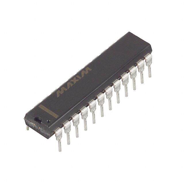
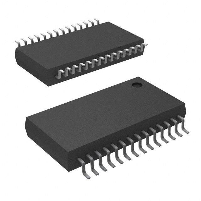
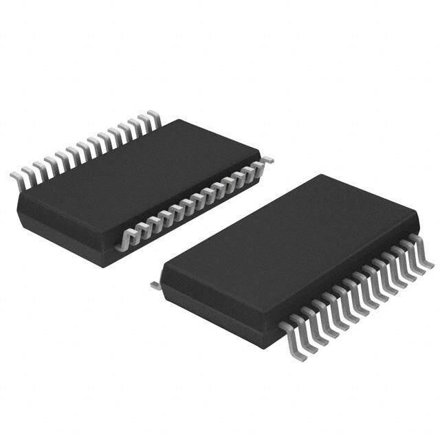
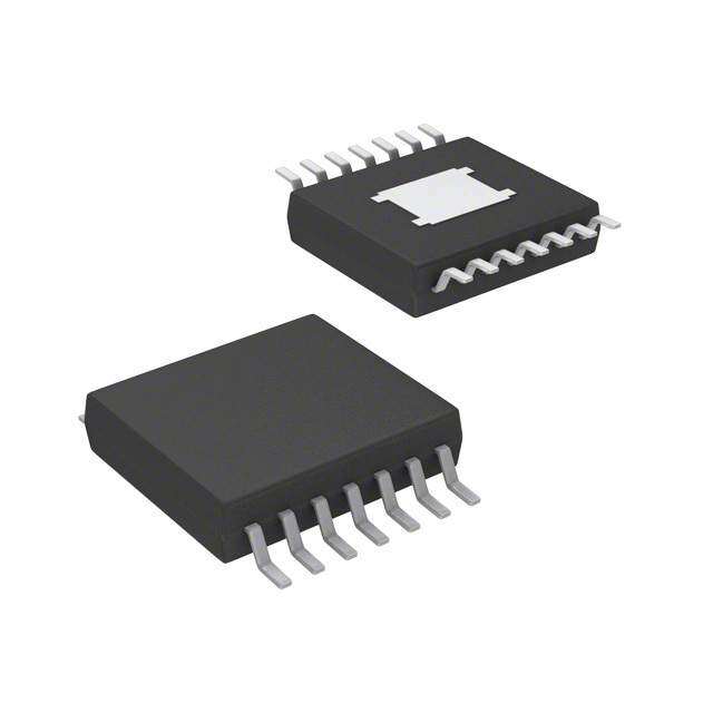
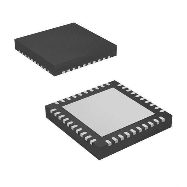
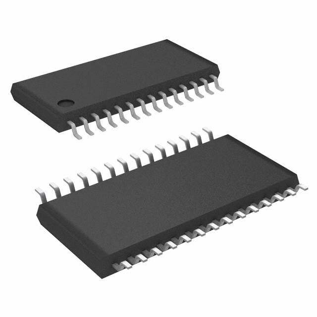
| 产品图片 |
|
| rohs | 符合RoHS无铅 / 符合限制有害物质指令(RoHS)规范要求 |
| 产品系列 | 逻辑集成电路,缓冲器和线路驱动器,STMicroelectronics ST3237EBPR- |
| 数据手册 | |
| 产品型号 | ST3237EBPR |
| 产品目录页面 | |
| 产品种类 | 缓冲器和线路驱动器 |
| 供应商器件封装 | 28-SSOP |
| 其它名称 | 497-7927-1 |
| 其它有关文件 | http://www.st.com/web/catalog/sense_power/FM1968/CL1179/SC392/PF66119?referrer=70071840 |
| 包装 | 剪切带 (CT) |
| 协议 | RS232 |
| 双工 | 全 |
| 商标 | STMicroelectronics |
| 安装类型 | 表面贴装 |
| 安装风格 | SMD/SMT |
| 封装 | Reel |
| 封装/外壳 | 28-SSOP(0.209",5.30mm 宽) |
| 封装/箱体 | SSOP-28 |
| 工作温度 | -40°C ~ 85°C |
| 工厂包装数量 | 1350 |
| 接口 | EIA/TIA-232. RS-232. V.24. V.28 |
| 接收器滞后 | 300mV |
| 数据速率 | 1Mbps |
| 最大工作温度 | + 85 C |
| 最小工作温度 | - 40 C |
| 标准包装 | 1 |
| 电压-电源 | 3 V ~ 5.5 V |
| 电源电压-最大 | 5.5 V |
| 电源电压-最小 | 3 V |
| 电源电流 | 1 mA |
| 类型 | 收发器 |
| 系列 | ST3237EB |
| 驱动器/接收器数 | 5/3 |






- 商务部:美国ITC正式对集成电路等产品启动337调查
- 曝三星4nm工艺存在良率问题 高通将骁龙8 Gen1或转产台积电
- 太阳诱电将投资9.5亿元在常州建新厂生产MLCC 预计2023年完工
- 英特尔发布欧洲新工厂建设计划 深化IDM 2.0 战略
- 台积电先进制程称霸业界 有大客户加持明年业绩稳了
- 达到5530亿美元!SIA预计今年全球半导体销售额将创下新高
- 英特尔拟将自动驾驶子公司Mobileye上市 估值或超500亿美元
- 三星加码芯片和SET,合并消费电子和移动部门,撤换高东真等 CEO
- 三星电子宣布重大人事变动 还合并消费电子和移动部门
- 海关总署:前11个月进口集成电路产品价值2.52万亿元 增长14.8%



PDF Datasheet 数据手册内容提取
ST3237EB ± 15 kV ESD protected, 1 µA, 3 to 5.5 V, 250 kbps RS-232 transceiver with stand-by Features ■ ESD protection for RS-232 I/O pins – ±15 kV human body model – ±8 kV IEC 1000-4-2 contacts discharge ■ 1 µA low power shutdown with receivers active ■ Guaranteed data rate – 250 kbps (normal operation) – 1 Mbps (very high speed operation) ■ Guaranteed slew rate range – 6 V/µs (normal operation) SSOP SOP – 24 V/µs (very high speed operation) ■ 0.1 µF external capacitors ■ Flow-through pinout ■ Low supply current 300 µA ■ Available in SSOP28 and SO-28 operation mode and 1 Mbps in the very high speed operation mode while maintaining RS-232 Description output levels. The ST3237E is a 3 V to 5.5 V powered EIA/TIA- 232 and V.28/V.24 communication interfaces high data-rate capability and enhanced electrostatic discharge (ESD) protection at ±8 kV using IEC1000-4-2 contact discharge and ±15 kV using Human Body Model (HBM). The other pins are protected with standard ESD protection at ±2 kV using HBM method. The ST3237C is a transceiver (5 drivers, 3 receivers) for fast modem applications. The device has a proprietary low-dropout transmitter output stage providing true RS-232 performance from a 3 V to 5.5 V supply using a dual charge pump. The device is guaranteed to run at data rates of 250 kbps in the normal Table 1. Device summary Temperature Order code Package Packaging range ST3237EBDR -40 to 85 °C SO-28 (tape and reel) 1000 parts per reel ST3237EBPR -40 to 85°C SSOP28 (tape and reel) 1350 parts per reel November 2007 Rev 7 1/18 www.st.com 18
Contents ST3237EB Contents 1 Pin configuration . . . . . . . . . . . . . . . . . . . . . . . . . . . . . . . . . . . . . . . . . . . 3 2 Absolute maximum ratings . . . . . . . . . . . . . . . . . . . . . . . . . . . . . . . . . . . 5 3 Electrical characteristics . . . . . . . . . . . . . . . . . . . . . . . . . . . . . . . . . . . . . 6 4 Application . . . . . . . . . . . . . . . . . . . . . . . . . . . . . . . . . . . . . . . . . . . . . . . . . 8 5 Typical performance characteristics . . . . . . . . . . . . . . . . . . . . . . . . . . . . 9 6 Application note . . . . . . . . . . . . . . . . . . . . . . . . . . . . . . . . . . . . . . . . . . . 10 7 Package mechanical data . . . . . . . . . . . . . . . . . . . . . . . . . . . . . . . . . . . . 12 8 Revision history . . . . . . . . . . . . . . . . . . . . . . . . . . . . . . . . . . . . . . . . . . . 17 2/18
ST3237EB Pin configuration 1 Pin configuration Figure 1. Pin connection Table 2. Pin description Pin n° Symbol Name and function 1 C + Positive Terminal of Inverting Charge Pump Capacitor 2 2 GND Ground 3 C - Negative terminal of inverting charge pump capacitor 2 4 V- 5.5V generated by the charge pump 5 T1 First transmitter output voltage OUT 6 T2 Second transmitter output voltage OUT 7 T3 Third transmitter output voltage OUT 8 R1 First receiver input voltage IN 9 R2 Second receiver input voltage IN 10 T4 Fourth transmitter output voltage OUT 11 R3 Third receiver input voltage IN 12 T5 Fifth transmitter output voltage OUT 13 EN Receiver enable, active low 14 SHDN Shutdown control, active low Very high speed control input. Connect to GND for normal 15 VHSCI operation; connect to V for 1 Mbps transmission rates. CC 16 R1 Non inverting complementary receiver output. Always active. OUTB 17 T5 Fifth transmitter input voltage IN 18 R3 Third receiver output voltage OUT 3/18
Pin configuration ST3237EB Table 2. Pin description (continued) Pin n° Symbol Name and function 19 T4 Fourth transmitter input voltage IN 20 R2 Second receiver output voltage OUT 21 R1 First receiver output voltage OUT 22 T3 Third transmitter input voltage IN 23 T2 Second transmitter input voltage IN 24 T1 First transmitter input voltage N 25 C - Negative terminal of voltage- charge pump capacitor 1 26 V Supply voltage CC 27 V+ -5.5V generated by the charge pump 28 C + Positive terminal of voltage- charge pump capacitor 1 4/18
ST3237EB Absolute maximum ratings 2 Absolute maximum ratings Table 3. Absolute maximum ratings Symbol Parameter Value Unit V Supply voltage -0.3 to 6 V CC V+ Doubled voltage terminal -0.3 to 7 V V- Inverted voltage terminal 0.3 to -7 V V+ +|V-| 13 V T Transmitter input voltage range -0.3 to 6 V IN SHDN, EN -0.3 to 6 V VHSCI Very high speed control input -0.3 to (V +0.3) V CC R Receiver input voltage range ± 25 V IN T Transmitter output voltage range ± 13.2 V OUT R , OUT Receiver output voltage range -0.3 to (V + 0.3) V R CC OUTB t Short circuit duration on T (one at a time) Continuous SHORT OUT T Storage temperature range -65 to 150 °C stg Note: Absolute maximum ratings are those values beyond which damage to the device may occur. Functional operation under these condition is not implied. V+ and V- can have a maximum magnitude of +7 V, but their absolute addition can not exceed 13 V. Table 4. Shutdown and enable control truth table SHDN EN T-OUT R-OUT R-OUTB 0 0 High Z Active Active 0 1 High Z High Z Active 1 0 Active Active Active 1 1 Active High Z Active Figure 2. ESD performance: transmitter outputs, receiver inputs Symbol Parameter Test conditions Min. Typ. Max. Unit ESD ESD protection voltage Human body model ±15 kV ESD ESD protection voltage IEC-1000-4-2 contact discharge ±8 kV 5/18
Electrical characteristics ST3237EB 3 Electrical characteristics Table 5. Electrical characteristics (C - C = 0.1 µF, V = 3 V to 5.5 V, T = -40 to 85 °C, unless 1 4 CC A otherwise specified. Typical values are referred to T = 25 °C) A Symbol Parameter Test conditions Min. Typ. Max. Unit I V power supply current SHDN=V , No Load 0.3 1 mA SUPPLY CC CC I Shutdown supply current SHDN=GND, V =GND or V 1 5 µA SHDN T_IN CC Table 6. Logic input (C - C = 0.1 µF, V = 3 V to 5.5 V, T = -40 to 85 °C, unless otherwise 1 4 CC A specified. Typical values are referred to T = 25 °C) A Symbol Parameter Test conditions Min. Typ. Max. Unit Input logic threshold low V T-IN, VHSCI, EN, SHDN 0.8 V TIL (1) V = 3.3V 2 CC V Input logic threshold high T-IN, VHSCI, EN, SHDN V TIH V = 5V 2.4 CC I Input leakage current T-IN, VHSCI, EN, SHDN ± 1.0 µA IL Transmitter input V 0.25 V HYS hysteresis 1. Transmitter input hysteresis is typically 250 mV Table 7. Transmitter (C - C = 0.1 µF tested at 3.3 V ± 10 %, V = 3 V to 5.5 V, T = -40 to 85 °C, 1 4 CC A unless otherwise specified. Typical values are referred to T = 25 °C) A Symbol Parameter Test conditions Min. Typ. Max. Unit All transmitter outputs are loaded with V Output voltage swing ± 5 ± 5.4 V TOUT 3KΩ to GND Transmitter output R V = 0V, V = ± 2V 300 10M Ω TOUT resistance CC OUT I Output short circuit current ± 60 mA SC V = 0V or 3.3V to 5.5V CC ITOL Output leakage current VOUT = ± 12V ± 25 µA Transmitters disable 6/18
ST3237EB Electrical characteristics Table 8. Receiver (C - C = 0.1 µF tested at 3.3 V ±10 %, V = 3 V to 5.5 V, T = -40 to 85 °C, 1 4 CC A unless otherwise specified. Typical values are referred to T = 25°C) A Symbol Parameter Test conditions Min. Typ. Max. Unit I Output leakage current Receiver disabled, EN = V ± 0.05 ± 10 µA OL CC V Output voltage low I = 1mA 0.4 V OL OUT V Output voltage high I = -1mA V -0.6 V -0.1 V OH OUT CC CC Receiver input voltage V -25 25 V RIN operating range RS-232 input threshold TA = 25°C, VCC = 3.3V 0.6 1.1 V V RIL low T = 25°C, V = 5V 0.8 1.5 A CC RS-232 input threshold TA = 25°C, VCC = 3.3V 1.5 2.4 V V RIH high T = 25°C, V = 5V 1.2 2.4 A CC V Input hysteresis 0.3 V RIHYS R Input resistance T = 25°C 3 5 7 KΩ RIN A Table 9. Timing characteristics (C - C = 0.1 µF tested at 3.3 V ±10 %, V = 3 V to 5.5 V, 1 4 CC T = -40 to 85 °C, unless otherwise specified. Typical values are referred to T = 25 °C) A A Symbol Parameter Test conditions Min. Typ. Max. Unit R = 3KΩ, C = 1000pF L L 250 Kbps one transmitter switching, VHSCI=GND R = 3KΩ, C = 250pF L L one transmitter switching, VHSCI=V 1000 Kbps D Maximum data rate CC R V = 3 to 4.5V CC R = 3KΩ, C = 1000pF L L one transmitter switching, VHSCI=V 1000 Kbps CC V = 4.5 to 5.5V CC t Propagation delay input to PHLR R to R , C = 150pF 0.15 µs t output IN OUT L PLHR R = 3kΩ, C = 1000pF, t Propagation delay input to L L ns PHLR VHSCI=V 400 t output CC ns PLHR VHSCI=GND 1000 |t - t |, VHSCI=GND 300 ns PHL TLH t Transmitter skew T_SKEW |t - t |, VHSCI=V 50 ns PHL TLH CC t Receiver skew |t - t | 100 ns R_SKEW PHL TLH t Receiver output enable time Normal operation 50 ns OER t Receiver output disable time Normal operation 120 ns ODR T = 25°C R = 3 to 7KΩ, V = 3.3V A L CC measured from +3V to -3V or -3V to +3V S Transition slew rate C = 150pF to 1000pF, VHSCI=GND 6 30 V/µs RT L C = 150pF to 1000pF, VHSCI=V 24 150 V/µs L CC C = 150pF to 2500pF, VHSCI=GND 4 30 V/µs L Note: Transmitter skew is measured at the transmitter zero cross points 7/18
Application ST3237EB 4 Application Figure 3. Application circuits Table 10. Capacitance value (µF) V C1 C2 C3 C4 Cbypass CC 3.0 to 3.6 0.22 0.22 0.22 0.22 0.1 3.1 to 3.6 0.1 0.1 0.1 0.1 0.1 4.5 to 5.5 0.047 0.33 0.33 0.33 0.1 3.0 to 5.5 0.22 0.1 0.1 0.1 0.1 8/18
ST3237EB Typical performance characteristics 5 Typical performance characteristics (unless otherwise specified T = 25°C) J Figure 4. Low level receiver output current Figure 5. High level receiver output current Figure 6. ESD protection Note: The high ESD protected pins are the I/O RS232 line, transmitter out and receiver in. The other pins guarantee ± 2 kV HBM ESD protection versus ground by means of diodes. 9/18
Application note ST3237EB 6 Application note This application note describes the procedure for determining the susceptibility and the test method to verify ST ESD advanced protection on RS-232 or RS485 I/O device. Static electricity is defined as an electrical charge caused by an imbalance of electrons on the surface of a material. This imbalance of electrons produces an electric field that can be measured and that can influence other objects at a distance. Electrostatic discharge is defined as the transfer of charge between bodies at different electrical potentials. Electrostatic discharge (ESD) can change the electrical characteristics of a semiconductor device, degrading or destroying it. Any input or output port (I/O) allows access communication with other pieces of equipment by external connectors. These connectors are directly linked by the I/O pins of RS-232 or RS485 interface. ST provides the E-series by advanced high ESD protection structure. The protection functionality is tested in two different conditions: The first model is used to simulate the HUMAN BODY MODEL (HBM) event. A similar discharge can occur from a charged conductive object, such as a metallic tool or fixture. The model used to characterize this event is known as the machine model. A human body model circuit and waveform is presented in figures below. Figure 7. Human body model circuit Figure 8. Human body model current waveform 10/18
ST3237EB Application note The second model is IEC 1000-4-2 and is used to simulate the reaction of the device on equipment when subjected to electrostatic discharges, which may occur from personnel to objects near vital instrumentation. Direct (Contact) and indirect (Air Gap) applications of discharges to the equipment under test (EUT) are possible. Test characteristics are shown in circuit, waveform and table below. Figure 9. IEC 1000-4-2 circuit Figure 10. IEC 1000-4-2 current waveform Table 11. Characteristics of the ESD generator First peak current Indicated Rise time with discharge Current at 30 ns Current at 60 ns Level of discharge (± voltage switch (± 30%) (± 30%) 10%) 1 2 kV 7.5 A 0.7 to 1ns 4 A 2 A 2 4 kV 15 A 0.7 to 1ns 8 A 4 A 3 6 kV 22.5 A 0.7 to 1ns 12 A 6 A 4 8 kV 30 A 0.7 to 1ns 16 A 8 A 11/18
Package mechanical data ST3237EB 7 Package mechanical data In order to meet environmental requirements, ST offers these devices in ECOPACK® packages. These packages have a lead-free second level interconnect. The category of second Level Interconnect is marked on the package and on the inner box label, in compliance with JEDEC Standard JESD97. The maximum ratings related to soldering conditions are also marked on the inner box label. ECOPACK is an ST trademark. ECOPACK specifications are available at: www.st.com. 12/18
ST3237EB Package mechanical data SO-28 mechanical data mm. inch. Dim. Min. Typ. Max. Min. Typ. Max. A 2.65 0.104 a1 0.1 0.3 0.004 0.012 b 0.35 0.49 0.014 0.019 b1 0.23 0.32 0.009 0.012 C 0.5 0.020 c1 45° (typ.) D 17.70 18.10 0.697 0.713 E 10.00 10.65 0.393 0.419 e 1.27 0.050 e3 16.51 0.650 F 7.40 7.60 0.291 0.300 L 0.50 1.27 0.020 0.050 S 8° (max.) 0016023 13/18
Package mechanical data ST3237EB SSOP28 mechanical data mm. inch. Dim. Min. Typ. Max. Min. Typ. Max. A 2 0.079 A1 0.050 0.002 A2 1.65 1.75 1.85 0.065 0.069 0.073 b 0.22 0.38 0.009 0.015 c 0.09 0.25 0.004 0.010 D 9.9 10.2 10.5 0.390 0.402 0.413 E 7.4 7.8 8.2 0.291 0.307 0.323 E1 5 5.3 5.6 0.197 0.209 0.220 e 0.65 BSC 0.0256 BSC K 0° 10° 0° 10° L 0.55 0.75 0.95 0.022 0.030 0.037 14/18
ST3237EB Package mechanical data Tape & reel SO-28 mechanical data mm. inch. Dim. Min. Typ. Max. Min. Typ. Max. A 330 12.992 C 12.8 13.2 0.504 0.519 D 20.2 0.795 N 60 2.362 T 30.4 1.197 Ao 10.8 11.0 0.425 0.433 Bo 18.2 18.4 0.716 0.724 Ko 2.9 3.1 0.114 0.122 Po 3.9 4.1 0.153 0.161 P 11.9 12.1 0.468 0.476 15/18
Package mechanical data ST3237EB Tape & reel SSOP28 mechanical data mm. inch. Dim. Min. Typ. Max. Min. Typ. Max. A 330 12.992 C 12.8 13.2 0.504 0.519 D 20.2 0.795 N 60 2.362 T 22.4 0.882 Ao 8.4 8.6 0.331 0.339 Bo 10.7 10.9 0.421 0.429 Ko 2.9 3.1 0.114 0.122 Po 3.9 4.1 0.153 0.161 P 11.9 12.1 0.468 0.476 16/18
ST3237EB Revision history 8 Revision history Table 12. Document revision history Date Revision Changes 21-Mar-2005 5 TSSOP has been removed. 24-Mar-2006 6 Order codes updated. 13-Nov-2007 7 Added Table1. 17/18
ST3237EB Please Read Carefully: Information in this document is provided solely in connection with ST products. STMicroelectronics NV and its subsidiaries (“ST”) reserve the right to make changes, corrections, modifications or improvements, to this document, and the products and services described herein at any time, without notice. All ST products are sold pursuant to ST’s terms and conditions of sale. Purchasers are solely responsible for the choice, selection and use of the ST products and services described herein, and ST assumes no liability whatsoever relating to the choice, selection or use of the ST products and services described herein. No license, express or implied, by estoppel or otherwise, to any intellectual property rights is granted under this document. If any part of this document refers to any third party products or services it shall not be deemed a license grant by ST for the use of such third party products or services, or any intellectual property contained therein or considered as a warranty covering the use in any manner whatsoever of such third party products or services or any intellectual property contained therein. UNLESS OTHERWISE SET FORTH IN ST’S TERMS AND CONDITIONS OF SALE ST DISCLAIMS ANY EXPRESS OR IMPLIED WARRANTY WITH RESPECT TO THE USE AND/OR SALE OF ST PRODUCTS INCLUDING WITHOUT LIMITATION IMPLIED WARRANTIES OF MERCHANTABILITY, FITNESS FOR A PARTICULAR PURPOSE (AND THEIR EQUIVALENTS UNDER THE LAWS OF ANY JURISDICTION), OR INFRINGEMENT OF ANY PATENT, COPYRIGHT OR OTHER INTELLECTUAL PROPERTY RIGHT. UNLESS EXPRESSLY APPROVED IN WRITING BY AN AUTHORIZED ST REPRESENTATIVE, ST PRODUCTS ARE NOT RECOMMENDED, AUTHORIZED OR WARRANTED FOR USE IN MILITARY, AIR CRAFT, SPACE, LIFE SAVING, OR LIFE SUSTAINING APPLICATIONS, NOR IN PRODUCTS OR SYSTEMS WHERE FAILURE OR MALFUNCTION MAY RESULT IN PERSONAL INJURY, DEATH, OR SEVERE PROPERTY OR ENVIRONMENTAL DAMAGE. ST PRODUCTS WHICH ARE NOT SPECIFIED AS "AUTOMOTIVE GRADE" MAY ONLY BE USED IN AUTOMOTIVE APPLICATIONS AT USER’S OWN RISK. Resale of ST products with provisions different from the statements and/or technical features set forth in this document shall immediately void any warranty granted by ST for the ST product or service described herein and shall not create or extend in any manner whatsoever, any liability of ST. ST and the ST logo are trademarks or registered trademarks of ST in various countries. Information in this document supersedes and replaces all information previously supplied. The ST logo is a registered trademark of STMicroelectronics. All other names are the property of their respective owners. © 2007 STMicroelectronics - All rights reserved STMicroelectronics group of companies Australia - Belgium - Brazil - Canada - China - Czech Republic - Finland - France - Germany - Hong Kong - India - Israel - Italy - Japan - Malaysia - Malta - Morocco - Singapore - Spain - Sweden - Switzerland - United Kingdom - United States of America www.st.com 18/18
Mouser Electronics Authorized Distributor Click to View Pricing, Inventory, Delivery & Lifecycle Information: S TMicroelectronics: ST3237EBPR ST3237EBDR

 Datasheet下载

