
 Datasheet下载
- 型号: SST39VF3201C-70-4I-EKE
- 制造商: Microchip
- 库位|库存: xxxx|xxxx
- 要求:
| 数量阶梯 | 香港交货 | 国内含税 |
| +xxxx | $xxxx | ¥xxxx |
查看当月历史价格
查看今年历史价格
SST39VF3201C-70-4I-EKE产品简介:
ICGOO电子元器件商城为您提供SST39VF3201C-70-4I-EKE由Microchip设计生产,在icgoo商城现货销售,并且可以通过原厂、代理商等渠道进行代购。 SST39VF3201C-70-4I-EKE价格参考。MicrochipSST39VF3201C-70-4I-EKE封装/规格:存储器, FLASH 存储器 IC 32Mb (2M x 16) 并联 70ns 48-TSOP。您可以下载SST39VF3201C-70-4I-EKE参考资料、Datasheet数据手册功能说明书,资料中有SST39VF3201C-70-4I-EKE 详细功能的应用电路图电压和使用方法及教程。
SST39VF3201C-70-4I-EKE 是由 Microchip Technology 生产的一款存储器芯片,属于闪存(Flash Memory)类别。其主要应用场景包括:

1. 嵌入式系统:该芯片常用于各种嵌入式设备中,如工业控制器、家用电器和消费电子产品。它提供非易失性存储功能,用于存储固件或程序代码。

2. 数据记录与日志:适用于需要频繁写入和读取数据的场景,例如数据记录仪、监控系统等。它可以可靠地保存关键数据,即使在断电情况下也不会丢失。

3. 网络设备:在网络路由器、交换机和其他通信设备中,这款芯片可用于存储引导程序(Bootloader)和操作系统镜像。

4. 汽车电子:在汽车行业中,该芯片可以用于车载娱乐系统、导航系统和发动机控制单元(ECU),以存储必要的软件和配置信息。

5. 医疗设备:在一些便携式或固定式医疗设备中,如监护仪、血糖仪等,这款芯片可以用来存储患者数据和设备参数。

6. 安全系统:在安防摄像头、门禁系统等安全设备中,SST39VF3201C 可用于存储加密密钥、访问权限信息以及系统设置。

其 32Mbit 的容量和较低的功耗特性,使其成为对存储需求不高但要求稳定性和低能耗的应用的理想选择。此外,其工作电压范围广(2.7V 至 3.6V),适应多种电源环境,进一步拓宽了其应用领域。
| 参数 | 数值 |
| 产品目录 | 集成电路 (IC)半导体 |
| 描述 | IC FLASH 32MBIT 70NS 48TSOP闪存 2.7V to 3.6V 32Mbit Multi-Prps Fl |
| 产品分类 | |
| 品牌 | Microchip Technology |
| 产品手册 | http://www.microchip.com/mymicrochip/filehandler.aspx?ddocname=en553532 |
| 产品图片 |
|
| rohs | 符合RoHS无铅 / 符合限制有害物质指令(RoHS)规范要求 |
| 产品系列 | 内存,闪存,Microchip Technology SST39VF3201C-70-4I-EKESST39 MPF™ |
| 数据手册 | http://www.microchip.com/mymicrochip/filehandler.aspx?ddocname=en553532 |
| 产品型号 | SST39VF3201C-70-4I-EKE |
| 产品种类 | 闪存 |
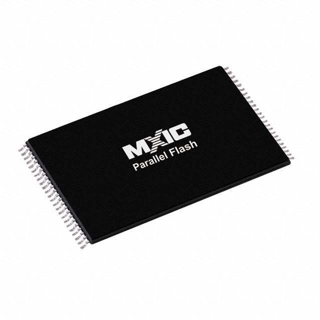
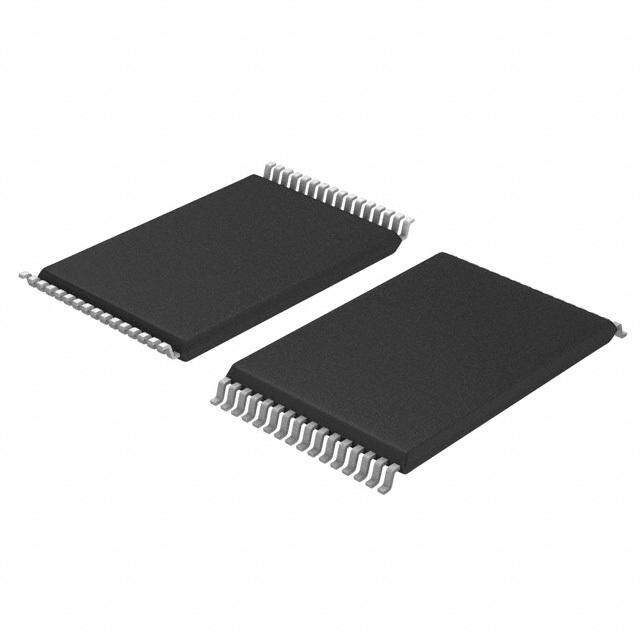
| 供应商器件封装 | 48-TSOP(12x20) |
| 其它名称 | SST39VF3201C704IEKE |
| 包装 | 托盘 |
| 商标 | Microchip Technology |
| 存储器类型 | FLASH |
| 存储容量 | 32 Mbit |
| 存储类型 | NOR |
| 安装风格 | SMD/SMT |
| 定时类型 | Asynchronous |
| 封装 | Tray |
| 封装/外壳 | 48-TFSOP(0.724",18.40mm 宽) |
| 封装/箱体 | TSOP-48 |
| 工作温度 | + 85 C |
| 工作温度范围 | - 40 C to + 85 C |
| 工厂包装数量 | 96 |
| 接口 | 并联 |
| 接口类型 | Parallel |
| 数据总线宽度 | 16 bit |
| 最大工作电流 | 15 mA |
| 标准包装 | 96 |
| 格式-存储器 | 闪存 |
| 电压-电源 | 2.7 V ~ 3.6 V |
| 电源电压-最大 | 3.6 V |
| 电源电压-最小 | 2.7 V |
| 系列 | SST39VF |
| 组织 | 2 M x 16 |
| 结构 | Sector |
| 访问时间 | 70 ns |
| 速度 | 70 ns |


_renders/IS45S16320F-7BLA1.jpg)


- 商务部:美国ITC正式对集成电路等产品启动337调查
- 曝三星4nm工艺存在良率问题 高通将骁龙8 Gen1或转产台积电
- 太阳诱电将投资9.5亿元在常州建新厂生产MLCC 预计2023年完工
- 英特尔发布欧洲新工厂建设计划 深化IDM 2.0 战略
- 台积电先进制程称霸业界 有大客户加持明年业绩稳了
- 达到5530亿美元!SIA预计今年全球半导体销售额将创下新高
- 英特尔拟将自动驾驶子公司Mobileye上市 估值或超500亿美元
- 三星加码芯片和SET,合并消费电子和移动部门,撤换高东真等 CEO
- 三星电子宣布重大人事变动 还合并消费电子和移动部门
- 海关总署:前11个月进口集成电路产品价值2.52万亿元 增长14.8%


_renders/IS42S32800D-6BLI.jpg)


PDF Datasheet 数据手册内容提取
32 Mbit (x16) Multi-Purpose Flash Plus SST39VF3201C / SST39VF3202C DataSheet The SST39VF3201C and SST39VF3202C devices are 2M x16, CMOS Multi-Pur- pose Flash Plus (MPF+) manufactured with proprietary, high performance CMOS SuperFlash technology. The split-gate cell design and thick-oxide tunneling injec- tor attain better reliability and manufacturability compared with alternate approaches. The SST39VF3201C and SST39VF3202C write (Program or Erase) with a 2.7-3.6V power supply. This device conforms to JEDEC standard pinouts for x16 memories. Features (cid:129) Organizedas2Mx16 (cid:129) Security-IDFeature –Microchip:128bits;User:128words (cid:129) SingleVoltageReadandWriteOperations –2.7-3.6V (cid:129) FastReadAccessTime: –70ns (cid:129) SuperiorReliability –Endurance:100,000Cycles(Typical) (cid:129) LatchedAddressandData –Greaterthan100yearsDataRetention (cid:129) FastEraseandWord-Program: (cid:129) LowPowerConsumption(typicalvaluesat5MHz) –Sector-EraseTime:18ms(typical) –ActiveCurrent:6mA(typical) –Block-EraseTime:18ms(typical) –StandbyCurrent:4µA(typical) –Chip-EraseTime:35ms(typical) –AutoLowPowerMode:4µA(typical) –Word-ProgramTime:7µs(typical) (cid:129) HardwareBlock-Protection/WP#InputPin (cid:129) AutomaticWriteTiming –TopBlock-Protection(toptwo4-KWordblocks) –InternalV Generation PP forSST39VF3202C –BottomBlock-Protection(bottomtwo4-KWordblocks) (cid:129) End-of-WriteDetection forSST39VF3201C –ToggleBits –Data#Polling (cid:129) Sector-EraseCapability –RY/BY#Pin –Uniform2KWordsectors (cid:129) CMOSI/OCompatibility (cid:129) Block-EraseCapability (cid:129) JEDECStandard –Flexibleblockarchitecture –Eight4-KWordblocks,6332-KWordblocks –FlashEEPROMPinAssignments (cid:129) Chip-EraseCapability (cid:129) PackagesAvailable –48-leadTSOP(12mmx20mm) (cid:129) Erase-Suspend/Erase-ResumeCapabilities –48-ballTFBGA(6mmx8mm) (cid:129) HardwareResetPin(RST#) (cid:129) AlldevicesareRoHScompliant www.microchip.com ©2014SiliconStorageTechnology,Inc. DS20005020B 07/14
32 Mbit Multi-Purpose Flash Plus SST39VF3201C / SST39VF3202C DataSheet Product Description The SST39VF3201C and SST39VF3202C devices are 2M x16 CMOS Multi-Purpose Flash Plus (MPF+) manufactured with proprietary, high-performance CMOS SuperFlash technology. The split- gate cell design and thick-oxide tunneling injector attain better reliability and manufacturability com- pared with alternate approaches. The SST39VF3201C/3202C write (Program or Erase) with a 2.7- 3.6Vpowersupply.ThesedevicesconformtoJEDECstandardpinassignmentsforx16memories. Featuring high performance Word-Program, the SST39VF3201C/3202C devices provide a typical Word-Program time of 7 µsec.These devices useToggle Bit, Data# Polling, or RY/BY# pin to indicate thecompletionofProgramoperation.Toprotectagainstinadvertentwrite,theyhaveon-chiphardware and Software Data Protection schemes. Designed, manufactured, and tested for a wide spectrum of applications, these devices are offered with a guaranteed typical endurance of 100,000 cycles. Data retentionisratedatgreaterthan100years. TheSST39VF3201C/3202Cdevicesaresuitedforapplicationsthatrequireconvenientandeconomical updating of program, configuration, or data memory. For all system applications, they significantly improve performance and reliability, while lowering power consumption. They inherently use less energyduringEraseandProgramthanalternativeflashtechnologies.Thetotalenergyconsumedisa functionoftheappliedvoltage,current,andtimeofapplication.Sinceforanygivenvoltagerange,the SuperFlash technology uses less current to program and has a shorter erase time, the total energy consumed during any Erase or Program operation is less than alternative flash technologies. These devices also improve flexibility while lowering the cost for program, data, and configuration storage applications. The SuperFlash technology provides fixed Erase and Program times, independent of the number of Erase/Program cycles that have occurred.Therefore the system software or hardware does not have to be modified or de-rated as is necessary with alternative flash technologies, whose Erase and Pro- gramtimesincreasewithaccumulatedErase/Programcycles. To meet high-density, surface mount requirements, the SST39VF3201C/3202C devices are offered in 48-leadTSOPand48-ballTFBGApackages.SeeFigure2andFigure3forpinassignments. ©2014SiliconStorageTechnology,Inc. DS20005020B 07/14 2
32 Mbit Multi-Purpose Flash Plus SST39VF3201C / SST39VF3202C DataSheet Block Diagram SuperFlash X-Decoder Memory MemoryAddress AddressBuffer Latches Y-Decoder CE# OE# WE# ControlLogic WP# RESET# I/OBuffersandDataLatches RY/BY# DQ15-DQ0 1410B1.0 Figure 1: Functional Block Diagram ©2014SiliconStorageTechnology,Inc. DS20005020B 07/14 3
32 Mbit Multi-Purpose Flash Plus SST39VF3201C / SST39VF3202C DataSheet Pin Assignments A15 1 48 A16 A14 2 47 NC A13 3 46 VSS A12 4 45 DQ15 A11 5 44 DQ7 A10 6 43 DQ14 A9 7 42 DQ6 A8 8 41 DQ13 A19 9 StandardPinout 40 DQ5 A20 10 39 DQ12 WE# 11 TopView 38 DQ4 RST# 12 37 VDD DieUp NC 13 36 DQ11 WP# 14 35 DQ3 RY/BY# 15 34 DQ10 A18 16 33 DQ2 A17 17 32 DQ9 A7 18 31 DQ1 A6 19 30 DQ8 A5 20 29 DQ0 A4 21 28 OE# A3 22 27 VSS A2 23 26 CE# A1 24 25 A0 141048-tsopEKP1.0 Figure 2: Pin Assignments for 48-leadTSOP TOPVIEW (ballsfacingdown) 6 A13 A12 A14 A15 A16 NC DQ15VSS 5 A9 A8 A10 A11 DQ7DQ14DQ13DQ6 4 WE# RST# NC A19 DQ5DQ12 VDD DQ4 3 RY/BY#WP# A18 A20 DQ2DQ10DQ11DQ3 2 A7 A17 A6 A5 DQ0 DQ8 DQ9 DQ1 1 A3 A4 A2 A1 A0 CE# OE# VSS A B C D E F G H 14104-tfbgaB1KP2.0 Figure 3: Pin assignments for 48-ballTFBGA ©2014SiliconStorageTechnology,Inc. DS20005020B 07/14 4
32 Mbit Multi-Purpose Flash Plus SST39VF3201C / SST39VF3202C DataSheet Table 1: Pin Description Symbol PinName Functions A 1-A AddressInputs Toprovidememoryaddresses. MS 0 DuringSector-EraseA -A addresslineswillselectthesector. MS 11 DuringBlock-EraseA -A addresslineswillselecttheblock. MS 15 DQ -DQ DataInput/output TooutputdataduringReadcyclesandreceiveinputdataduringWritecycles. 15 0 DataisinternallylatchedduringaWritecycle. Theoutputsareintri-statewhenOE#orCE#ishigh. WP# WriteProtect Toprotectthetop/bottombootblockfromErase/Programoperationwhen grounded. RST# Reset ToresetandreturnthedevicetoReadmode. CE# ChipEnable ToactivatethedevicewhenCE#islow. OE# OutputEnable Togatethedataoutputbuffers. WE# WriteEnable TocontroltheWriteoperations. V PowerSupply Toprovidepowersupplyvoltage:2.7-3.6V DD V Ground SS NC NoConnection Unconnectedpins. RY/BY# Ready/Busy# TooutputthestatusofaProgramorEraseoperation RY/BY#isaopendrainoutput,soa10K-100Kpull-upresistorisrequired toallowRY/BY#totransitionhighindicatingthedeviceisreadytoread. T1.020005020 1. AMS=Mostsignificantaddress AMS=A20forSST39VF3201C/3202C ©2014SiliconStorageTechnology,Inc. DS20005020B 07/14 5
32 Mbit Multi-Purpose Flash Plus SST39VF3201C / SST39VF3202C DataSheet Table 2: Top / Bottom Boot Block Address (1 of 2) TopBootBlockAddressSST39VF3202C BottomBootBlockAddressSST39VF3201C Size Size # AddressRange # AddressRange (KWord) (KWord) 70 4 1FF000H-1FFFFFH 70 32 1F8000H-1FFFFFH 69 4 1FE000H-1FEFFFH 69 32 1F0000H-1F7FFFH 68 4 1FD000H-1FDFFFH 68 32 1E8000H-1EFFFFH 67 4 1FC000H-1FCFFFH 67 32 1E0000H-1E7FFFH 66 4 1FB000H-1FBFFFH 66 32 1D8000H-1DFFFFH 65 4 1FA000H-1FAFFFH 65 32 1D0000H-1D7FFFH 64 4 1F9000H-1F9FFFH 64 32 1C8000H-1CFFFFH 63 4 1F8000H-1F8FFFH 63 32 1C0000H-1C7FFFH 62 32 1F0000H-1F7FFFH 62 32 1B8000H-1BFFFFH 61 32 1E8000H-1EFFFFH 61 32 1B0000H-1B7FFFH 60 32 1E0000H-1E7FFFH 60 32 1A8000H-1AFFFFH 59 32 1D8000H-1DFFFFH 59 32 1A0000H-1A7FFFH 58 32 1D0000H-1D7FFFH 58 32 198000H-19FFFFH 57 32 1C8000H-1CFFFFH 57 32 190000H-197FFFH 56 32 1C0000H-1C7FFFH 56 32 188000H-18FFFFH 55 32 1B8000H-1BFFFFH 55 32 180000H-187FFFH 54 32 1B0000H-1B7FFFH 54 32 178000H-17FFFFH 53 32 1A8000H-1AFFFFH 53 32 170000H-177FFFH 52 32 1A0000H-1A7FFFH 52 32 168000H-16FFFFH 51 32 198000H-19FFFFH 51 32 160000H-167FFFH 50 32 190000H-197FFFH 50 32 158000H-15FFFFH 49 32 188000H-18FFFFH 49 32 150000H-157FFFH 48 32 180000H-187FFFH 48 32 148000H-14FFFFH 47 32 178000H-17FFFFH 47 32 140000H-147FFFH 46 32 170000H-177FFFH 46 32 138000H-13FFFFH 45 32 168000H-16FFFFH 45 32 130000H-137FFFH 44 32 160000H-167FFFH 44 32 128000H-12FFFFH 43 32 158000H-15FFFFH 43 32 120000H-127FFFH 42 32 150000H-157FFFH 42 32 118000H-11FFFFH 41 32 148000H-14FFFFH 41 32 110000H-117FFFH 40 32 140000H-147FFFH 40 32 108000H-10FFFFH 39 32 138000H-13FFFFH 39 32 100000H-107FFFH 38 32 130000H-137FFFH 38 32 0F8000H-0FFFFFH 37 32 128000H-12FFFFH 37 32 0F0000H-0F7FFFH 36 32 120000H-127FFFH 36 32 0E8000H-0EFFFFH 35 32 118000H-11FFFFH 35 32 0E0000H-0E7FFFH 34 32 110000H-117FFFH 34 32 0D8000H-0DFFFFH 33 32 108000H-10FFFFH 33 32 0D0000H-0D7FFFH 32 32 100000H-107FFFH 32 32 0C8000H-0CFFFFH 31 32 0F8000H-0FFFFFH 31 32 0C0000H-0C7FFFH ©2014SiliconStorageTechnology,Inc. DS20005020B 07/14 6
32 Mbit Multi-Purpose Flash Plus SST39VF3201C / SST39VF3202C DataSheet Table 2: Top / Bottom Boot Block Address (Continued) (2 of 2) 30 32 0F0000H-0F7FFFH 30 32 0B8000H-0BFFFFH 29 32 0E8000H-0EFFFFH 29 32 0B0000H-0B7FFFH 28 32 0E0000H-0E7FFFH 28 32 0A8000H-0AFFFFH 27 32 0D8000H-0DFFFFH 27 32 0A0000H-0A7FFFH 26 32 0D0000H-0D7FFFH 26 32 098000H-09FFFFH 25 32 0C8000H-0CFFFFH 25 32 090000H-097FFFH 24 32 0C0000H-0C7FFFH 24 32 088000H-08FFFFH 23 32 0B8000H-0BFFFFH 23 32 080000H-087FFFH 22 32 0B0000H-0B7FFFH 22 32 078000H-07FFFFH 21 32 0A8000H-0AFFFFH 21 32 070000H-077FFFH 20 32 0A0000H-0A7FFFH 20 32 068000H-06FFFFH 19 32 098000H-09FFFFH 19 32 060000H-067FFFH 18 32 090000H-097FFFH 18 32 058000H-05FFFFH 17 32 088000H-08FFFFH 17 32 050000H-057FFFH 16 32 080000H-087FFFH 16 32 048000H-04FFFFH 15 32 078000H-07FFFFH 15 32 040000H-047FFFH 14 32 070000H-077FFFH 14 32 038000H-03FFFFH 13 32 068000H-06FFFFH 13 32 030000H-037FFFH 12 32 060000H-067FFFH 12 32 028000H-02FFFFH 11 32 058000H-05FFFFH 11 32 020000H-027FFFH 10 32 050000H-057FFFH 10 32 018000H-01FFFFH 9 32 048000H-04FFFFH 9 32 010000H-017FFFH 8 32 040000H-047FFFH 8 32 008000H-00FFFFH 7 32 038000H-03FFFFH 7 4 007000H-007FFFH 6 32 030000H-037FFFH 6 4 006000H-006FFFH 5 32 028000H-02FFFFH 5 4 005000H-005FFFH 4 32 020000H-027FFFH 4 4 004000H-004FFFH 3 32 018000H-01FFFFH 3 4 003000H-003FFFH 2 32 010000H-017FFFH 2 4 002000H-002FFFH 1 32 008000H-00FFFFH 1 4 001000H-001FFFH 0 32 000000H-007FFFH 0 4 000000H-000FFFH T2.20005020 ©2014SiliconStorageTechnology,Inc. DS20005020B 07/14 7
32 Mbit Multi-Purpose Flash Plus SST39VF3201C / SST39VF3202C DataSheet Device Operation Commands are used to initiate the memory operation functions of the device. Commands are written tothedeviceusingstandardmicroprocessorwritesequences.AcommandiswrittenbyassertingWE# low while keeping CE# low.The address bus is latched on the falling edge ofWE# or CE#, whichever occurslast.ThedatabusislatchedontherisingedgeofWE#orCE#,whicheveroccursfirst. The SST39VF3201C/3202C also have the Auto Low Power mode which puts the device in a near standby mode after data has been accessed with a valid Read operation.This reduces the I active DD read current from typically 9 mA to typically 4 µA.The Auto Low Power mode reduces the typical I DD activereadcurrenttotherangeof2mA/MHzofReadcycletime.ThedeviceexitstheAutoLowPower mode with any address transition or control signal transition used to initiate another Read cycle, with noaccesstimepenalty.NotethatthedevicedoesnotenterAuto-LowPowermodeafterpower-upwith CE#heldsteadilylow,untilthefirstaddresstransitionorCE#isdrivenhigh. Read The Read operation of the SST39VF3201C/3202Cis controlled by CE# and OE#, both have to be low forthesystemtoobtaindatafromtheoutputs.CE#isusedfordeviceselection.WhenCE#ishigh,the chipisdeselectedandonlystandbypowerisconsumed.OE#istheoutputcontrolandisusedtogate data from the output pins.The data bus is in high impedance state when either CE# or OE# is high. RefertotheReadcycletimingdiagramforfurtherdetails(Figure5). Word-Program Operation TheSST39VF3201C/3202Careprogrammedonaword-by-wordbasis.Beforeprogramming,thesector where the word exists must be fully erased. The Program operation is accomplished in three steps. Thefirststepisthethree-byteloadsequenceforSoftwareDataProtection.Thesecondstepistoload word address and word data. During the Word-Program operation, the addresses are latched on the falling edge of either CE# or WE#, whichever occurs last. The data is latched on the rising edge of eitherCE#orWE#,whicheveroccursfirst.ThethirdstepistheinternalProgramoperationwhichisini- tiated after the rising edge of the fourthWE# or CE#, whichever occurs first.The Program operation, once initiated, will be completed within 10 µs. See Figure 6 and Figure 7 forWE# and CE# controlled Program operation timing diagrams and Figure 21 for flowcharts. During the Program operation, the only valid reads are Data# Polling and Toggle Bit. During the internal Program operation, the host is free to perform additional tasks. Any commands issued during the internal Program operation are ignored.Duringthecommandsequence,WP#shouldbestaticallyheldhighorlow. Sector/Block-Erase Operation TheSector-(orBlock-)Eraseoperationallowsthesystemtoerasethedeviceonasector-by-sector(or block-by-block)basis.TheSST39VF3201C/3202CofferbothSector-EraseandBlock-Erasemode.The sector architecture is based on uniform sector size of 2 KWord. The Block-Erase mode is based on block sizes of 4 and 32 KWord. The Sector-Erase operation is initiated by executing a six-byte com- mandsequencewithSector-Erasecommand(50H)andsectoraddress(SA)inthelastbuscycle.The Block-Erase operation is initiated by executing a six-byte command sequence with Block-Erase com- mand(30H)andblockaddress(BA)inthelastbuscycle.Thesectororblockaddressislatchedonthe falling edge of the sixthWE# pulse, while the command (50H or 30H) is latched on the rising edge of thesixthWE#pulse.TheinternalEraseoperationbeginsafterthesixthWE#pulse.TheEnd-of-Erase operationcanbedeterminedusingeitherData#PollingorToggleBitmethods.SeeFigure11andFig- ure12fortimingwaveformsandFigure25fortheflowchart.AnycommandsissuedduringtheSector- ©2014SiliconStorageTechnology,Inc. DS20005020B 07/14 8
32 Mbit Multi-Purpose Flash Plus SST39VF3201C / SST39VF3202C DataSheet orBlock-Eraseoperationareignored.WhenWP#islow,anyattempttoSector-(Block-)Erasethepro- tectedblockwillbeignored.Duringthecommandsequence,WP#shouldbestaticallyheldhighorlow. Erase-Suspend/Erase-Resume Commands The Erase-Suspend operation temporarily suspends a Sector- or Block-Erase operation thus allowing datatobereadfromanymemorylocation,orprogramdataintoanysector/blockthatisnotsuspended foranEraseoperation.TheoperationisexecutedbyissuingonebytecommandsequencewithErase- Suspend command (B0H).The device automatically enters read mode typically within 10 µs after the Erase-Suspendcommandhadbeenissued.Validdatacanbereadfromanysectororblockthatisnot suspended from an Erase operation. Reading at address location within erase-suspended sectors/ blockswilloutputDQ togglingandDQ at‘1’.WhileinErase-Suspendmode,aWord-Programopera- 2 6 tionisallowedexceptforthesectororblockselectedforErase-Suspend. To resume Sector-Erase or Block-Erase operation which has been suspended the system must issue Erase Resume command. The operation is executed by issuing one byte command sequence with EraseResumecommand(30H)atanyaddressinthelastBytesequence. Chip-Erase Operation TheSST39VF3201C/3202CprovideaChip-Eraseoperation,whichallowstheusertoerasetheentire memoryarraytothe“1”state.Thisisusefulwhentheentiredevicemustbequicklyerased. The Chip-Erase operation is initiated by executing a six-byte command sequence with Chip-Erase command(10H)ataddress555Hinthelastbytesequence.TheEraseoperationbeginswiththerising edgeofthesixthWE#orCE#,whicheveroccursfirst.DuringtheEraseoperation,theonlyvalidreadis ToggleBitorData#Polling.SeeTable7forthecommandsequence,Figure10fortimingdiagram,and Figure25fortheflowchart.AnycommandsissuedduringtheChip-Eraseoperationareignored.When WP# is low, any attempt to Chip-Erase will be ignored. During the command sequence, WP# should bestaticallyheldhighorlow. Write Operation Status Detection The SST39VF3201C/3202Cprovide two software means to detect the completion of aWrite (Program or Erase) cycle, in order to optimize the system write cycle time.The software detection includes two status bits: Data# Polling (DQ ) and Toggle Bit (DQ ). The End-of-Write detection mode is enabled 7 6 aftertherisingedgeofWE#,whichinitiatestheinternalProgramorEraseoperation. The actual completion of the nonvolatile write is asynchronous with the system; therefore, either a Data# Polling or Toggle Bit read may be simultaneous with the completion of the write cycle. If this occurs, the system may possibly get an erroneous result, i.e., valid data may appear to conflict with either DQ or DQ . In order to prevent spurious rejection, if an erroneous result occurs, the software 7 6 routine should include a loop to read the accessed location an additional two (2) times. If both reads arevalid,thenthedevicehascompletedtheWritecycle,otherwisetherejectionisvalid. ©2014SiliconStorageTechnology,Inc. DS20005020B 07/14 9
32 Mbit Multi-Purpose Flash Plus SST39VF3201C / SST39VF3202C DataSheet Data# Polling (DQ ) 7 When the SST39VF3201C/3202C are in the internal Program operation, any attempt to read DQ will 7 producethecomplementofthetruedata.OncetheProgramoperationiscompleted,DQ willproduce 7 truedata.NotethateventhoughDQ mayhavevaliddataimmediatelyfollowingthecompletionofaninternal 7 Writeoperation,theremainingdataoutputsmaystillbeinvalid:validdataontheentiredatabuswillappearin subsequentsuccessiveReadcyclesafteranintervalof1µs.During internal Erase operation, any attempt toreadDQ willproducea‘0’.OncetheinternalEraseoperationiscompleted,DQ willproducea‘1’. 7 7 TheData#PollingisvalidaftertherisingedgeoffourthWE#(orCE#)pulseforProgramoperation.For Sector-, Block- or Chip-Erase, the Data# Polling is valid after the rising edge of sixth WE# (or CE#) pulse.SeeFigure8forData#PollingtimingdiagramandFigure22foraflowchart. Toggle Bits (DQ6 and DQ2) During the internal Program or Erase operation, any consecutive attempts to read DQ will produce 6 alternating“1”sand“0”s,i.e.,togglingbetween1and0.WhentheinternalProgramorEraseoperation iscompleted,theDQ bitwillstoptoggling.Thedeviceisthenreadyforthenextoperation.ForSector- 6 , Block-, or Chip-Erase, the toggle bit (DQ ) is valid after the rising edge of sixthWE# (or CE#) pulse. 6 DQ will be set to ‘1’ if a Read operation is attempted on an Erase-Suspended Sector/Block. If Pro- 6 gramoperationisinitiatedinasector/blocknotselectedinErase-Suspendmode,DQ willtoggle. 6 An additional Toggle Bit is available on DQ , which can be used in conjunction with DQ to check 2 6 whetheraparticularsectorisbeingactivelyerasedorerase-suspended.Table3showsdetailedstatus bits information.TheToggle Bit (DQ ) is valid after the rising edge of the last WE# (or CE#) pulse of 2 Writeoperation.SeeFigure9forToggleBittimingdiagramandFigure22foraflowchart. Table 3: Write Operation Status Status DQ DQ DQ RY/BY# 7 6 2 NormalOperation StandardProgram DQ7# Toggle No 0 Toggle StandardErase 0 Toggle Toggle 0 Erase-Suspend ReadfromErase-Sus- 1 1 Toggle 1 Mode pendedSector/Block ReadfromNon-Erase- Data Data Data 1 SuspendedSector/Block Program DQ7# Toggle N/A 0 T3.0 20005020 Note: DQ7,DQ6andDQ2requireavalidaddresswhenreadingstatusinformation. ©2014SiliconStorageTechnology,Inc. DS20005020B 07/14 10
32 Mbit Multi-Purpose Flash Plus SST39VF3201C / SST39VF3202C DataSheet Ready/Busy# (RY/BY#) The devices include a Ready/Busy# (RY/BY#) output signal. RY/BY# is an open drain output pin that indicates whether an Erase or Program operation is in progress. Since RY/BY# is an open drain out- put,itallowsseveraldevicestobetiedinparalleltoV viaanexternalpull-upresistor.Aftertherising DD edgeofthefinalWE#pulseinthecommandsequence,theRY/BY#statusisvalid. When RY/BY# is actively pulled low, it indicates that an Erase or Program operation is in progress. WhenRY/BY#ishigh(Ready),thedevicesmaybereadorleftinstandbymode. Data Protection The SST39VF3201C/3202C provide both hardware and software features to protect nonvolatile data frominadvertentwrites. Hardware Data Protection Noise/GlitchProtection:AWE#orCE#pulseoflessthan5nswillnotinitiateawritecycle. V PowerUp/DownDetection:TheWriteoperationisinhibitedwhenV islessthan1.5V. DD DD Write Inhibit Mode: Forcing OE# low, CE# high, orWE# high will inhibit theWrite operation.This pre- ventsinadvertentwritesduringpower-uporpower-down. Hardware Block Protection The SST39VF3202C support top hardware block protection, which protects the top two 4-KWord blocks of the device. The SST39VF3201C support bottom hardware block protection, which protects thebottomtwo4-KWordblocksofthedevice.TheBootBlockaddressrangesaredescribedinTable4. Program and Erase operations are prevented on the two 4-KWord blocks whenWP# is low. IfWP# is left floating, it is internally held high via a pull-up resistor, and the Boot Block is unprotected, enabling ProgramandEraseoperationsonthatblock. Table 4: Boot Block Address Ranges Product AddressRange BottomBootBlock SST39VF3201C 000000H-001FFFH TopBootBlock SST39VF3202C 1FE000H-1FFFFFH T4.020005020 Hardware Reset (RST#) TheRST#pinprovidesahardwaremethodofresettingthedevicetoreadarraydata.WhentheRST# pinisheldlowforatleastT anyin-progressoperationwillterminateandreturntoReadmode.When RP, no internal Program/Erase operation is in progress, a minimum period ofT is required after RST# RHR isdrivenhighbeforeavalidReadcantakeplace.SeeFigure17. The Erase or Program operation that has been interrupted needs to be re-initiated after the device resumesnormaloperationmodetoensuredataintegrity. ©2014SiliconStorageTechnology,Inc. DS20005020B 07/14 11
32 Mbit Multi-Purpose Flash Plus SST39VF3201C / SST39VF3202C DataSheet Software Data Protection (SDP) TheSST39VF3201C/3202CprovidetheJEDECapprovedSoftwareDataProtectionschemeforalldata alteration operations, i.e., Program and Erase. Any Program operation requires the inclusion of the three-byte sequence.The three-byte load sequence is used to initiate the Program operation, provid- ing optimal protection from inadvertent Write operations, e.g., during the system power-up or power- down. Any Erase operation requires the inclusion of six-byte sequence. These devices are shipped with the Software Data Protection permanently enabled. See Table 7 for the specific software com- mand codes. During SDP command sequence, invalid commands will abort the device to read mode withinT ThecontentsofDQ -DQ canbeV orV ,butnoothervalue,duringanySDPcommand RC. 15 8 IL IH sequence. Common Flash Memory Interface (CFI) The SST39VF3201C/3202C also contain the CFI information to describe the characteristics of the device.InordertoentertheCFIQuerymode,thesystemmustwritethethree-bytesequence,sameas productIDentrycommandwith98H(CFIQuerycommand)toaddress555Hinthelastbytesequence. ThesystemcanalsoentertheCFIQuerymode,byusingtheone-bytesequencewith55HonAddress and 98H on Data Bus. Once the device enters the CFI Query mode, the system can read CFI data at theaddressesgiveninTables8through10.ThesystemmustwritetheCFIExitcommandtoreturnto ReadmodefromtheCFIQuerymode. Product Identification The Product Identification mode identifies the devices as the SST39VF3201Cand SST39VF3202C, and the manufacturer as Microchip.This mode may be accessed through software operations. Users may use the Software Product Identification operation to identify the part (i.e., using the device ID) when usingmultiplemanufacturersinthesamesocket.Fordetails,seeTable7forsoftwareoperation,Figure 13 for the Software ID Entry and Read timing diagram and Figure 23 for the Software ID Entry com- mandsequenceflowchart. Table 5: Product Identification Address Data Manufacturer’sID 0000H BFH DeviceID SST39VF3201C 0001H 235F SST39VF3202C 0001H 235E T5.0 20005020 Product Identification Mode Exit/CFI Mode Exit InordertoreturntothestandardReadmode,theSoftwareProductIdentificationmodemustbeexited. Exit is accomplished by issuing the Software ID Exit command sequence, which returns the device to theReadmode.ThiscommandmayalsobeusedtoresetthedevicetotheReadmodeafteranyinad- vertenttransientconditionthatapparentlycausesthedevicetobehaveabnormally,e.g.,notreadcor- rectly. Please note that the Software ID Exit/CFI Exit command is ignored during an internal Program orEraseoperation.SeeTable7forsoftwarecommandcodes,Figure15fortimingwaveform,andFig- ure23andFigure24forflowcharts. ©2014SiliconStorageTechnology,Inc. DS20005020B 07/14 12
32 Mbit Multi-Purpose Flash Plus SST39VF3201C / SST39VF3202C DataSheet Security ID The SST39VF3201C/3202C devices offer a 136 word Security ID space. The Secure ID space is divided into two segments - one factory programmed segment and one user programmed segment. The first segment is programmed and locked at Microchip with a random 128-bit number. The 128- wordusersegmentisleftun-programmedforthecustomertoprogramasdesired. To program the user segment of the Security ID, the user must use the Security ID Word-Program command.Todetectend-of-writefortheSECID,readthetogglebits.DonotuseData#Polling.Once this is complete, the Sec ID should be locked using the User Sec ID Program Lock-Out.This disables anyfuturecorruptionofthisspace.NotethatregardlessofwhetherornottheSecIDislocked,neither SecIDsegmentcanbeerased. TheSecureIDspacecanbequeriedbyexecutingathree-bytecommandsequencewithEnterSecID command (88H) at address 555H in the last byte sequence.To exit this mode, the Exit Sec ID com- mandshouldbeexecuted.RefertoTable7formoredetails. ©2014SiliconStorageTechnology,Inc. DS20005020B 07/14 13
32 Mbit Multi-Purpose Flash Plus SST39VF3201C / SST39VF3202C DataSheet Operations Table 6: Operation Modes Selection Mode CE# OE# WE# DQ Address Read V V V D A IL IL IH OUT IN Program V V V D A IL IH IL IN IN Erase V V V X1 Sectororblockaddress, IL IH IL XXHforChip-Erase Standby V X X HighZ X IH WriteInhibit X V X HighZ/D X IL OUT X X V HighZ/D X IH OUT ProductIdentification SoftwareMode V V V SeeTable7 IL IL IH T6.020005020 1. XcanbeVILorVIH,butnoothervalue. Table 7: Software Command Sequence Command 1stBus 2ndBus 3rdBus 4thBus 5thBus 6thBus Sequence WriteCycle WriteCycle WriteCycle WriteCycle WriteCycle WriteCycle Addr1 Data2 Addr1 Data2 Addr1 Data2 Addr1 Data2 Addr1 Data2 Addr1 Data2 Word-Program 555H AAH 2AAH 55H 555H A0H WA3 Data Sector-Erase 555H AAH 2AAH 55H 555H 80H 555H AAH 2AAH 55H SA 4 50H X Block-Erase 555H AAH 2AAH 55H 555H 80H 555H AAH 2AAH 55H BA 4 30H X Chip-Erase 555H AAH 2AAH 55H 555H 80H 555H AAH 2AAH 55H 555H 10H Erase-Suspend XXXXH B0H Erase-Resume XXXXH 30H QuerySecID5 555H AAH 2AAH 55H 555H 88H UserSecurityID 555H AAH 2AAH 55H 555H A5H WA6 Data Word-Program UserSecurityID 555H AAH 2AAH 55H 555H 85H XXH6 0000H ProgramLock-Out SoftwareID 555H AAH 2AAH 55H 555H 90H Entry7,8 CFIQueryEntry 555H AAH 2AAH 55H 555H 98H CFIQueryEntry 55H 98H SoftwareIDExit9,10 555H AAH 2AAH 55H 555H F0H /CFIExit/SecID Exit SoftwareIDExit9,10 XXH F0H /CFIExit/SecID Exit T7.020005020 1. AddressformatA10-A0(Hex). AddressesA11-A20canbeVILorVIH,butnoothervalue,forCommandsequenceforSST39VF3201C/3202C. 2. DQ15-DQ8canbeVILorVIH,butnoothervalue,forCommandsequence 3. WA=ProgramWordaddress 4. SAXforSector-Erase;usesAMS-A11addresslines BAX,forBlock-Erase;usesAMS-A15addresslines AMS=Mostsignificantaddress AMS=A20forSST39VF3201C/3202C ©2014SiliconStorageTechnology,Inc. DS20005020B 07/14 14
32 Mbit Multi-Purpose Flash Plus SST39VF3201C / SST39VF3202C DataSheet 5. WithAMS-A4=0; SecIDisreadwithA3-A0, MicrochipIDisreadwithA3=0(Addressrange=000000Hto000007H), UserIDisreadwithA3=1(Addressrange=000008Hto000087H). LockStatusisreadwithA7-A0=0000FFH.Unlocked:DQ3=1/Locked:DQ3=0. 6. ValidWord-AddressesforSecIDarefrom000000H-000007Hand000008Hto000087H. 7. ThedevicedoesnotremaininSoftwareProductIDModeifpowereddown. 8. ForManufactureID WithAMS-A0=0;MicrochipManufacturerID=00BFHisread ForDeviceID- DeviceIDcanbereadeitherinonecycle(address01H)orinthreecycles(addresses01H,0EHand0FH) One-cyclemethod- WithAMS-A1=0,A0=1;Microchip39VF3201C/3202CDeviceID=235F/235Eisread Three-cyclemethod- WithAMS-A1=0,A0=1;SST39VF3201C/3202CDeviceID=235F/235Eisread(cycle1) WithAMS-A4=0;A3-A1=1;A0=0;SST39VF3201C/3202CDeviceIDadditionalinfo=1A/1Aisread(Note:1A=32Mbit) (cycle2) WithAMS-A4=0;A3-A0=1;SST39VF3201C/3202CDeviceIDadditionalinfo=00/01isread(00/01=Bottom/TopBoot) (cycle3) AMS=Mostsignificantaddress AMS=A20forSST39VF3201C/3202C 9. BothSoftwareIDExitoperationsareequivalent 10. Ifusersneverlockafterprogramming,SecIDcanbeprogrammedoverthepreviouslyunprogrammedbits(data=1) usingtheSecIDmodeagain(theprogrammed“0”bitscannotbereversedto“1”).ValidWord-AddressesforSecIDare from000000H-000007Hand000008Hto000087H. Table 8: CFI Query Identification String1 for SST39VF3201C/3202C Address Data Data 10H 0051H QueryUniqueASCIIstring“QRY” 11H 0052H 12H 0059H 13H 0002H PrimaryOEMcommandset 14H 0000H 15H 0000H AddressforPrimaryExtendedTable 16H 0000H 17H 0000H AlternateOEMcommandset(00H=noneexists) 18H 0000H 19H 0000H AddressforAlternateOEMextendedTable(00H=noneexits) 1AH 0000H T8.020005020 1. RefertoCFIpublication100formoredetails. ©2014SiliconStorageTechnology,Inc. DS20005020B 07/14 15
32 Mbit Multi-Purpose Flash Plus SST39VF3201C / SST39VF3202C DataSheet Table 9: System Interface Information for SST39VF3201C/3202C Address Data Data 1BH 0027H V Min(Program/Erase) DD DQ -DQ :Volts,DQ -DQ :100millivolts 7 4 3 0 1CH 0036H V Max(Program/Erase) DD DQ -DQ :Volts,DQ -DQ :100millivolts 7 4 3 0 1DH 0000H V min.(00H=noV pin) PP PP 1EH 0000H V max.(00H=noV pin) PP PP 1FH 0003H TypicaltimeoutforWord-Program2Nµs(23=8µs) 20H 0000H Typicaltimeoutformin.sizebufferprogram2Nµs(00H=notsupported) 21H 0004H TypicaltimeoutforindividualSector/Block-Erase2Nms(24=16ms) 22H 0005H TypicaltimeoutforChip-Erase2Nms(25=32ms) 23H 0001H MaximumtimeoutforWord-Program2Ntimestypical(21x23=16µs) 24H 0000H Maximumtimeoutforbufferprogram2Ntimestypical 25H 0001H MaximumtimeoutforindividualSector/Block-Erase2Ntimestypical(21x24=32ms) 26H 0001H MaximumtimeoutforChip-Erase2Ntimestypical(21x25=64ms) T9.0 20005020 Table 10:Device Geometry Information for SST39VF3201C/3202C Address Data Data 27H 0016H Devicesize=2NBytes(16H=22;222=4MByte) 28H 0001H FlashDeviceInterfacedescription;0001H=x16-onlyasynchronousinterface 29H 0000H 2AH 0000H Maximumnumberofbytesinmulti-bytewrite=2N(00H=notsupported) 2BH 0000H 2CH 0003H NumberofEraseSector/Blocksizessupportedbydevice 2DH 0007H EraseBlock1regioninformation. 2EH 0000H 2FH 0020H 30H 0000H 31H 003EH EraseBlock2regioninformation. 32H 0000H 33H 0000H 34H 0001H 35H 0000H EraseBlock3regioninformation. 36H 0000H 37H 0000H 38H 0000H 39H 0000H EraseBlock4regioninformation. 3AH 0000H 3BH 0000H 3CH 0000H T10.020005020 ©2014SiliconStorageTechnology,Inc. DS20005020B 07/14 16
32 Mbit Multi-Purpose Flash Plus SST39VF3201C / SST39VF3202C DataSheet AbsoluteMaximumStressRatings (Applied conditions greater than those listed under “Absolute MaximumStressRatings”maycausepermanentdamagetothedevice.Thisisastressratingonlyand functional operation of the device at these conditions or conditions greater than those defined in the operationalsectionsofthisdatasheetisnotimplied.Exposuretoabsolutemaximumstressratingcon- ditionsmayaffectdevicereliability.) TemperatureUnderBias .............................................. -55°Cto+125°C StorageTemperature ................................................ -65°Cto+150°C D.C.VoltageonAnyPintoGroundPotential .............................-0.5VtoV +0.5V DD TransientVoltage(<20ns)onAnyPintoGroundPotential ..................-2.0VtoV +2.0V DD VoltageonA PintoGroundPotential .....................................-0.5Vto13.2V 9 PackagePowerDissipationCapability(T =25°C)................................... 1.0W A SurfaceMountSolderReflowTemperature............................ 260°Cfor10seconds OutputShortCircuitCurrent1 .................................................. 50mA 1. Outputsshortedfornomorethanonesecond.Nomorethanoneoutputshortedatatime. Table 11:Operating Range Range AmbientTemp V DD Commercial 0°Cto+70°C 2.7-3.6V Industrial -40°Cto+85°C 2.7-3.6V T11.120005020 Table 12:AC Conditions ofTest1 InputRise/FallTime OutputLoad 5ns C =30pF L T12.120005020 1. SeeFigures19and20 ©2014SiliconStorageTechnology,Inc. DS20005020B 07/14 17
32 Mbit Multi-Purpose Flash Plus SST39VF3201C / SST39VF3202C DataSheet Power Up Specifications All functionalities and DC specifications are specified for aV ramp rate of greater than 1V per 100 DD ms (0V to 3V in less than 300 ms). If the VDD ramp rate is slower than 1V per 100 ms, a hardware reset is required.The recommendedV power-up to RESET# high time should be greater than 100 DD µstoensureaproperreset. TPU-READ 100µs VDD VDDmin 0V VIH RESET# TRHR 50ns CE# 1410F24.0 Figure 4: Power-Up Diagram Table 13:DC Operating CharacteristicsV = 2.7-3.6V1 DD Limits Symbol Parameter Min Max Units TestConditions I PowerSupplyCurrent Address input=V /V 2, at f=5 MHz, DD ILT IHT V =V Max DD DD Read3 15 mA CE#=V ,OE#=WE#=V ,allI/Osopen IL IH ProgramandErase 45 mA CE#=WE#=V ,OE#=V IL IH I StandbyV Current 50 µA CE#=V ,V =V Max SB DD IHC DD DD I AutoLowPower 50 µA CE#=V ,V =V Max ALP ILC DD DD Allinputs=V orV WE#=V SS DD, IHC I InputLeakageCurrent 1 µA V =GNDtoV ,V =V Max LI IN DD DD DD I InputLeakageCurrent 10 µA WP#=GNDtoV orRST#=GNDtoV LIW DD DD onWP#pinandRST# I OutputLeakageCurrent 1 µA V =GNDtoV ,V =V Max LO OUT DD DD DD V InputLowVoltage 0.8 V V =V Min IL DD DD V InputLowVoltage(CMOS) 0.3 V V =V Max ILC DD DD V InputHighVoltage 0.7V V V =V Max IH DD DD DD V InputHighVoltage(CMOS) V -0.3 V V =V Max IHC DD DD DD V OutputLowVoltage 0.2 V I =100µA,V =V Min OL OL DD DD V OutputHighVoltage V -0.2 V I =-100µA,V =V Min OH DD OH DD DD T13.0 20005020 1. TypicalconditionsfortheActiveCurrentshownonthefrontpageofthedatasheetareaveragevaluesat25°C (roomtemperature),andVDD=3V.Not100%tested. 2. SeeFigure19 3. TheIDDcurrentlistedistypicallylessthan2mA/MHz,withOE#atVIH.TypicalVDDis3V. ©2014SiliconStorageTechnology,Inc. DS20005020B 07/14 18
32 Mbit Multi-Purpose Flash Plus SST39VF3201C / SST39VF3202C DataSheet Table 14:Recommended System Power-upTimings Symbol Parameter Minimum Units T 1 Power-uptoReadOperation 100 µs PU-READ T 1 Power-uptoProgram/EraseOperation 100 µs PU-WRITE T14.020005020 1. Thisparameterismeasuredonlyforinitialqualificationandafteradesignorprocesschangethatcouldaffectthisparameter. Table 15:Capacitance (TA = 25°C, f=1 Mhz, other pins open) Parameter Description TestCondition Maximum C 1 I/OPinCapacitance V =0V 10pF I/O I/O C 1 InputCapacitance V =0V 10pF IN IN T15.020005020 1. Thisparameterismeasuredonlyforinitialqualificationandafteradesignorprocesschangethatcouldaffectthisparameter. Table 16:Reliability Characteristics Symbol Parameter MinimumSpecification Units TestMethod N 1,2 Endurance 10,000 Cycles JEDECStandardA117 END T 1 DataRetention 100 Years JEDECStandardA103 DR I 1 LatchUp 100+I mA JEDECStandard78 LTH DD T16.020005020 1. Thisparameterismeasuredonlyforinitialqualificationandafteradesignorprocesschangethatcouldaffectthisparameter. 2. NENDenduranceratingisqualifiedasa10,000cycleminimumforthewholedevice.Asector-orblock-levelratingwould resultinahigherminimumspecification. ©2014SiliconStorageTechnology,Inc. DS20005020B 07/14 19
32 Mbit Multi-Purpose Flash Plus SST39VF3201C / SST39VF3202C DataSheet AC Characteristics Table 17:Read CycleTiming ParametersV = 2.7-3.6V DD Symbol Parameter Min Max Units T ReadCycleTime 70 ns RC T ChipEnableAccessTime 70 ns CE T AddressAccessTime 70 ns AA T OutputEnableAccessTime 35 ns OE T 1 CE#LowtoActiveOutput 0 ns CLZ T 1 OE#LowtoActiveOutput 0 ns OLZ T 1 CE#HightoHigh-ZOutput 16 ns CHZ T 1 OE#HightoHigh-ZOutput 16 ns OHZ T 1 OutputHoldfromAddressChange 0 ns OH T 1 RST#PulseWidth 500 ns RP T 1 RST#HighbeforeRead 50 ns RHR T 1,2 RST#PinLowtoReadMode 20 µs RY T17.020005020 1. Thisparameterismeasuredonlyforinitialqualificationandafteradesignorprocesschangethatcouldaffectthisparameter. 2. ThisparameterappliestoSector-Erase,Block-Erase,andProgramoperations. ThisparameterdoesnotapplytoChip-Eraseoperations. Table 18:Program/Erase CycleTiming Parameters Symbol Parameter Min Max Units T Word-ProgramTime 10 µs BP T AddressSetupTime 0 ns AS T AddressHoldTime 30 ns AH T WE#andCE#SetupTime 0 ns CS T WE#andCE#HoldTime 0 ns CH T OE#HighSetupTime 0 ns OES T OE#HighHoldTime 10 ns OEH T CE#PulseWidth 40 ns CP T WE#PulseWidth 40 ns WP T 1 WE#PulseWidthHigh 30 ns WPH T 1 CE#PulseWidthHigh 30 ns CPH T DataSetupTime 30 ns DS T 1 DataHoldTime 0 ns DH T 1 SoftwareIDAccessandExitTime 150 ns IDA T Sector-Erase 25 ms SE T Block-Erase 25 ms BE T Chip-Erase 50 ms SCE T 1,2 RY/BY#DelayTime 90 ns BY T 1 BusRecoveryTime 0 µs BR T18.020005020 1. Thisparameterismeasuredonlyforinitialqualificationandafteradesignorprocesschangethatcouldaffectthisparameter. 2. ThisparameterappliestoSector-Erase,Block-Erase,andProgramoperations. ©2014SiliconStorageTechnology,Inc. DS20005020B 07/14 20
32 Mbit Multi-Purpose Flash Plus SST39VF3201C / SST39VF3202C DataSheet TRC TAA ADDRESSAMS-0 TCE CE# TOE OE# TOLZ TOHZ VIH WE# TCLZ TOH TCHZ HIGH-Z HIGH-Z DQ15-0 DATAVALID DATAVALID 1410F03.0 Note: AMS=Mostsignificantaddress AMS=A20forSST39VF3201C/3202C Figure 5: Read CycleTiming Diagram TBP ADDRESSES 555 2AA 555 ADDR TAH TWP WE# TAS TWPH OE# TCH CE# TCS TBY TBR RY/BY# TDS TDH DQ15-0 XXAA XX55 XXA0 DATA VALID WORD (ADDR/DATA) 1410F04.0 Note: WP#mustbeheldinproperlogicstate(VILor VIH)1µspriortoand1µsafterthecommandsequence. XcanbeVILorVIH,butnoothervalue. Figure 6: WE# Controlled Program CycleTiming Diagram ©2014SiliconStorageTechnology,Inc. DS20005020B 07/14 21
32 Mbit Multi-Purpose Flash Plus SST39VF3201C / SST39VF3202C DataSheet TBP ADDRESSES 555 2AA 555 ADDR TAH TCP WE# TAS TCPH OE# TCH CE# TCS TBY TBR RY/BY# TDS TDH DQ15-0 XXAA XX55 XXA0 DATA VALID WORD (ADDR/DATA) 1410F05.0 Note: WP#mustbeheldinproperlogicstate(VILorVIH)1µspriortoand1µsafterthecommandsequence. XcanbeVILorVIH,butnoothervalue. Figure 7: CE# Controlled Program CycleTiming Diagram ADDRESSA19-0-AMS-0 TCE CE# TOEH TOES OE# TOE WE# TBY RY/BY# DQ7 DATA DATA# DATA# DATA 1410F06.0 Note: AMS=Mostsignificantaddress AMS=A20forSST39VF3201C/3202C Figure 8: Data# PollingTiming Diagram ©2014SiliconStorageTechnology,Inc. DS20005020B 07/14 22
32 Mbit Multi-Purpose Flash Plus SST39VF3201C / SST39VF3202C DataSheet ADDRESSAMS-0 TCE CE# TOEH TOE TOES OE# WE# DQ6andDQ2 TWOREADCYCLES WITHSAMEOUTPUTS 1410F07.0 Note: AMS=Mostsignificantaddress AMS=A20forSST39VF3201C/3202C Figure 9: Toggle BitsTiming Diagram SIX-BYTECODEFORCHIP-ERASE TSCE ADDRESSES 555 2AA 555 555 2AA 555 CE# OE# TOEH WE# TBY TBR RY/BY# DQ15-0 XXAA XX55 XX80 XXAA XX55 XX10 VALID 1410F08.0 Note: ThisdevicealsosupportsCE#controlledChip-EraseoperationTheWE#andCE#signalsare interchangeableaslongasminimumtimingsaremet.(SeeTable18) WP#mustbeheldinproperlogicstate(VILorVIH)1µspriortoand1µsafterthecommandsequence. XcanbeVILorVIH,butnoothervalue. Figure 10:WE# Controlled Chip-EraseTiming Diagram ©2014SiliconStorageTechnology,Inc. DS20005020B 07/14 23
32 Mbit Multi-Purpose Flash Plus SST39VF3201C / SST39VF3202C DataSheet SIX-BYTECODEFORBLOCK-ERASE TBE ADDRESSES 555 2AA 555 555 2AA BAX CE# OE# TWP WE# TBY TBR RY/BY# DQ15-0 XXAA XX55 XX80 XXAA XX55 XX30 VALID 1410F09.0 Note: ThisdevicealsosupportsCE#controlledBlock-Eraseoperation.TheWE#andCE#signalsareinter- changeableaslongasminimumtimingsaremet.(SeeTable18). BAX=BlockAddress WP#mustbeheldinproperlogicstate(VILorVIH)1µspriortoand1µsafterthecommandsequence. XcanbeVILorVIH,butnoothervalue. Figure 11:WE# Controlled Block-EraseTiming Diagram SIX-BYTECODEFORSECTOR-ERASE TSE ADDRESSES 555 2AA 555 555 2AA SAX CE# OE# TWP WE# TBY TBR RY/BY# DQ15-0 XXAA XX55 XX80 XXAA XX55 XX50 VALID 1410F10.0 Note: ThisdevicealsosupportsCE#controlledSector-Eraseoperation.TheWE#andCE#signalsareinter- changeableaslongasminimumtimingsaremet.(SeeTable18). SAX=BlockAddress WP#mustbeheldinproperlogicstate(VILorVIH)1µspriortoand1µsafterthecommandsequence. XcanbeVILorVIH,butnoothervalue. Figure 12:WE# Controlled Sector-EraseTiming Diagram ©2014SiliconStorageTechnology,Inc. DS20005020B 07/14 24
32 Mbit Multi-Purpose Flash Plus SST39VF3201C / SST39VF3202C DataSheet Three-ByteSequenceforSoftwareIDEntry ADDRESS 555 2AA 555 0000 0001 CE# OE# TWP TIDA WE# TWPH TAA DQ15-0 XXAA XX55 XX90 00BF DeviceID SW0 SW1 SW2 1410F11.0 Note: DeviceID=235EforSST39VF3201Cand235EforSST39VF3202C WP#mustbeheldinproperlogicstate(VILorVIH)1µspriortoand1µsafterthecommandsequence. XcanbeVILorVIH,butnoothervalue. Figure 13:Software ID Entry and Read Three-ByteSequenceforCFIQueryEntry ADDRESS 555 2AA 555 CE# OE# TWP TIDA WE# TWPH TAA DQ15-0 XXAA XX55 XX98 SW0 SW1 SW2 1410F12.0 Note: WP#mustbeheldinproperlogicstate(VILorVIH)1µspriortoand1µsafterthecommandsequence. XcanbeVILorVIH,butnoothervalue. Figure 14:CFI Query Entry and Read ©2014SiliconStorageTechnology,Inc. DS20005020B 07/14 25
32 Mbit Multi-Purpose Flash Plus SST39VF3201C / SST39VF3202C DataSheet THREE-BYTESEQUENCEFOR SOFTWAREIDEXITANDRESET ADDRESSA14-0 555 2AA 555 DQ15-0 XXAA XX55 XXF0 TIDA CE# OE# TWP WE# TWHP SW0 SW1 SW2 1410F13.0 Note: WP#mustbeheldinproperlogicstate(VILorVIH)1µspriortoand1µsafterthecommandsequence. XcanbeVILorVIH,butnoothervalue. Figure 15:Software ID Exit/CFI Exit THREE-BYTESEQUENCEFOR CFIQUERYENTRY ADDRESSAMS-0 555 2AA 555 CE# OE# TWP TIDA WE# TWPH TAA DQ15-0 XXAA XX55 XX88 SW0 SW1 SW2 1410F14.0 Note: AMS=Mostsignificantaddress AMS=A20forSST39VF3201C/3202C WP#mustbeheldinproperlogicstate(VILorVIH)1µspriortoand1µsafterthecommandsequence. XcanbeVILorVIH,butnoothervalue. Figure 16:Sec ID Entry ©2014SiliconStorageTechnology,Inc. DS20005020B 07/14 26
32 Mbit Multi-Purpose Flash Plus SST39VF3201C / SST39VF3202C DataSheet RY/BY# 0V TRP RST# TRHR CE#/OE# 1410F15.0 Figure 17:RST#Timing Diagram (When no internal operation is in progress) TRY RY/BY# TRP RST# CE# TBR OE# 1410F16.0 Figure 18:RST#Timing Diagram (During Program or Erase operation) ©2014SiliconStorageTechnology,Inc. DS20005020B 07/14 27
32 Mbit Multi-Purpose Flash Plus SST39VF3201C / SST39VF3202C DataSheet VIHT INPUT VIT REFERENCEPOINTS VOT OUTPUT VILT 1410F17.0 ACtestinputsaredrivenatV (0.9V )foralogic“1”andV (0.1V )foralogic“0”.Measure- IHT DD ILT DD mentreferencepointsforinputsandoutputsareV (0.5V )andV (0.5V ).Inputriseandfall IT DD OT DD times(10%90%)are<5ns. Note: VIT-VINPUTTest VOT-VOUTPUTTest VIHT-VINPUTHIGHTest VILT-VINPUTLOWTest Figure 19:AC Input/Output ReferenceWaveforms TOTESTER TODUT CL 1410F18.0 Figure 20:ATest Load Example ©2014SiliconStorageTechnology,Inc. DS20005020B 07/14 28
32 Mbit Multi-Purpose Flash Plus SST39VF3201C / SST39VF3202C DataSheet Start Loaddata:XXAAH Address:555H Loaddata:XX55H Address:2AAH Loaddata:XXA0H Address:555H LoadWord Address/Word Data Waitforendof Program(TBP, Data#Polling bit,orTogglebit operation) Program Completed XcanbeVILorVIH,butnoothervalue 1410F19.0 Figure 21:Word-Program Algorithm ©2014SiliconStorageTechnology,Inc. DS20005020B 07/14 29
32 Mbit Multi-Purpose Flash Plus SST39VF3201C / SST39VF3202C DataSheet InternalTimer ToggleBit Data# Polling RY/BY# Program/Erase Program/Erase Program/Erase Program/Erase Initiated Initiated Initiated Initiated WaitTBP, Readword ReadDQ7 ReadRY/BY# TSCE,TSE orTBE Readsame No IsDQ7= No Is word truedata Program/Erase RY/BY#=1 Completed Yes Yes No DoesDQ6 Program/Erase match Completed Program/Erase Completed Yes Program/Erase Completed 1410F20.0 Figure 22:Wait Options ©2014SiliconStorageTechnology,Inc. DS20005020B 07/14 30
32 Mbit Multi-Purpose Flash Plus SST39VF3201C / SST39VF3202C DataSheet CFIQueryEntry SecIDQueryEntry SoftwareProductIDEntry CommandSequence CommandSequence CommandSequence Loaddata:XXAAH Loaddata:XX98H Loaddata:XXAAH Loaddata:XXAAH Address:555H Address:55H Address:555H Address:555H Loaddata:XX55H Loaddata:XX55H Loaddata:XX55H WaitTIDA Address:2AAH Address:2AAH Address:2AAH Loaddata:XX98H Loaddata:XX88H Loaddata:XX90H ReadCFIdata Address:555H Address:555H Address:555H WaitTIDA WaitTIDA WaitTIDA ReadCFIdata ReadSecID ReadSoftwareID XcanbeVILorVIH,butnoothervalue 1410F21.0 Figure 23:Software ID/CFI Entry Command Flowcharts ©2014SiliconStorageTechnology,Inc. DS20005020B 07/14 31
32 Mbit Multi-Purpose Flash Plus SST39VF3201C / SST39VF3202C DataSheet SoftwareIDExit/CFIExit/SecIDExit CommandSequence Loaddata:XXAAH Loaddata:XXF0H Address:555H Address:XXH Loaddata:XX55H WaitTIDA Address:2AAH Loaddata:XXF0H Returntonormal Address:555H operation WaitTIDA Returntonormal operation XcanbeVILorVIH,butnoothervalue 1410F22.0 Figure 24:Software ID/CFI Exit Command Flowcharts ©2014SiliconStorageTechnology,Inc. DS20005020B 07/14 32
32 Mbit Multi-Purpose Flash Plus SST39VF3201C / SST39VF3202C DataSheet Chip-Erase Sector-Erase Block-Erase CommandSequence CommandSequence CommandSequence Loaddata:XXAAH Loaddata:XXAAH Loaddata:XXAAH Address:555H Address:555H Address:555H Loaddata:XX55H Loaddata:XX55H Loaddata:XX55H Address:2AAH Address:2AAH Address:2AAH Loaddata:XX80H Loaddata:XX80H Loaddata:XX80H Address:555H Address:555H Address:555H Loaddata:XXAAH Loaddata:XXAAH Loaddata:XXAAH Address:555H Address:555H Address:555H Loaddata:XX55H Loaddata:XX55H Loaddata:XX55H Address:2AAH Address:2AAH Address:2AAH Loaddata:XX10H Loaddata:XX50H Loaddata:XX30H Address:555H Address:SAX Address:BAX WaitTSCE WaitTSE WaitTBE Chiperased Sectorerased Blockerased toFFFFH toFFFFH toFFFFH XcanbeVILorVIH,butnoothervalue 1410F23.0 Figure 25:Erase Command Sequence ©2014SiliconStorageTechnology,Inc. DS20005020B 07/14 33
32 Mbit Multi-Purpose Flash Plus SST39VF3201C / SST39VF3202C DataSheet Product Ordering Information SST 39 VF 3201C - 70 - 4I - EKE XX XX XXXXX - XX - XX - XXX EnvironmentalAttribute E1=non-Pb PackageModifier K=48ballsorleads PackageType E=TSOP(type1,dieup,12mmx 20mm) B3=TFBGA(6mmx8mm,0.8mm pitch) TemperatureRange C=Commercial=0°Cto+70°C I=Industrial=-40°Cto+85°C MinimumEndurance 4=10,000cycles ReadAccessSpeed 70=70ns HardwareBlockProtection 1=BottomBoot-Block 2=TopBoot-Block DeviceDensity 320=32Mbit Voltage V=2.7-3.6V ProductSeries 39=Multi-PurposeFlashPlus 1. Environmentalsuffix“E”denotesnon-Pbsolder. non-Pbsolderdevicesare“RoHSCompliant”. Valid Combinations for SST39VF3201C SST39VF3201C-70-4I-EKE SST39VF3201C-70-4I-B3KE SST39VF3201C-70-4C-EKE SST39VF3201C-70-4C-B3KE Valid Combinations for SST39VF3202C SST39VF3202C-70-4I-EKE SST39VF3202C-70-4I-B3KE SST39VF3202C-70-4C-EKE SST39VF3202C-70-4C-B3KE Note:Validcombinationsarethoseproductsinmassproductionorwillbeinmassproduction.ConsultyourMicro- chipsalesrepresentativetoconfirmavailabilityofvalidcombinationsandtodetermineavailabilityofnew combinations. ©2014SiliconStorageTechnology,Inc. DS20005020B 07/14 34
32 Mbit Multi-Purpose Flash Plus SST39VF3201C / SST39VF3202C DataSheet Packaging Diagrams 1.05 0.95 Pin#1Identifier 0.50 BSC 0.27 12.20 0.17 11.80 0.15 18.50 0.05 18.30 DETAIL 1.20 max. 0.70 0.50 20.20 0°-5° 19.80 0.70 Note: 1. ComplieswithJEDECpublication95MO-142DDdimensions, 0.50 althoughsomedimensionsmaybemorestringent. 2. Alllineardimensionsareinmillimeters(max/min). 1mm 3. Coplanarity:0.1mm 4. Maximumallowablemoldflashis0.15mmatthepackageends,and0.25mmbetweenleads. 48-tsop-EK-8 Figure 26:48-leadThin Small Outline Package (TSOP) 12mm x 20mm, Package Code: EK ©2014SiliconStorageTechnology,Inc. DS20005020B 07/14 35
32 Mbit Multi-Purpose Flash Plus SST39VF3201C / SST39VF3202C DataSheet TOP VIEW BOTTOM VIEW 8.00 ± 0.10 5.60 0.80 0.45 ± 0.05 (48X) 6 6 5 5 4 4.00 4 6.00 ± 0.10 3 3 2 2 1 1 0.80 A B C D E F G H H G F E D C B A A1 CORNER A1 CORNER SIDE VIEW 1.10 ± 0.10 0.12 SEATING PLANE 0.35 ± 0.05 1mm Note: 1. Complies with JEDEC Publication 95, MO-210, variant 'AB-1', although some dimensions may be more stringent. 2. All linear dimensions are in millimeters. 3. Coplanarity: 0.12 mm 4. Ball opening size is 0.38 mm (± 0.05 mm) 48-tfbga-B3K-6x8-450mic-5 Figure 27:48-ballThin-profile, Fine-pitch Ball Grid Array (TFBGA) 6mm x 8mm, Package Code: B3K ©2014SiliconStorageTechnology,Inc. DS20005020B 07/14 36
32 Mbit Multi-Purpose Flash Plus SST39VF3201C / SST39VF3202C DataSheet Table 19:Revision History Number Description Date 00 (cid:129) Initialrelease Nov2009 01 (cid:129) RevisedI andI inTable13onpage18 Aug2010 SB ALP A (cid:129) Appliednewdocumentformat Jun2011 (cid:129) Releaseddocumentunderletterrevisionsystem (cid:129) UpdatedspecnumberfromS71410toDS25020 B (cid:129) UpdateddocumentstatustoDataSheet Jul2014 ISBN:978-1-63276-425-6 ©2014MicrochipTechnologyInc. SST,SiliconStorageTechnology,theSSTlogo,SuperFlash,andMTPareregisteredtrademarksofMicrochipTechnology,Inc. MPF,SQI,SerialQuadI/O,andZ-ScalearetrademarksofMicrochipTechnology,Inc.Allothertrademarksandregisteredtrade- marksmentionedhereinarethepropertyoftheirrespectiveowners. Specificationsaresubjecttochangewithoutnotice.Refertowww.microchip.comforthemostrecentdocumentation.Forthemostcurrent packagedrawings,pleaseseethePackagingSpecificationlocatedathttp://www.microchip.com/packaging. Memorysizesdenoterawstoragecapacity;actualusablecapacitymaybeless. MicrochipmakesnowarrantyfortheuseofitsproductsotherthanthoseexpresslycontainedintheStandardTermsandConditions ofSale. Forsalesofficelocationsandinformation,pleaseseewww.microchip.com. www.microchip.com ©2014SiliconStorageTechnology,Inc. DS20005020B 07/14 37
Mouser Electronics Authorized Distributor Click to View Pricing, Inventory, Delivery & Lifecycle Information: M icrochip: SST39VF3201C-70-4I-B3KE SST39VF3201C-70-4I-B3KE-T SST39VF3201C-70-4I-EKE SST39VF3201C-70-4I-EKE- T SST39VF3202C-70-4I-B3KE SST39VF3202C-70-4I-B3KE-T SST39VF3202C-70-4I-EKE SST39VF3202C-70-4I- EKE-T