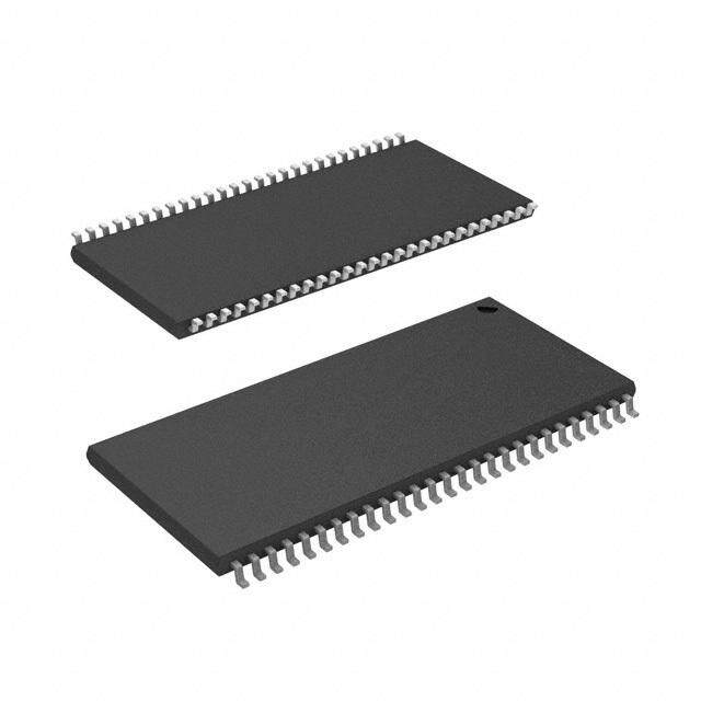
- 型号: SST25VF010A-33-4C-SAE
- 制造商: Microchip
- 库位|库存: xxxx|xxxx
- 要求:
| 数量阶梯 | 香港交货 | 国内含税 |
| +xxxx | $xxxx | ¥xxxx |
查看当月历史价格
查看今年历史价格
SST25VF010A-33-4C-SAE产品简介:
ICGOO电子元器件商城为您提供SST25VF010A-33-4C-SAE由Microchip设计生产,在icgoo商城现货销售,并且可以通过原厂、代理商等渠道进行代购。 SST25VF010A-33-4C-SAE价格参考。MicrochipSST25VF010A-33-4C-SAE封装/规格:存储器, FLASH 存储器 IC 1Mb (128K x 8) SPI 33MHz 8-SOIC。您可以下载SST25VF010A-33-4C-SAE参考资料、Datasheet数据手册功能说明书,资料中有SST25VF010A-33-4C-SAE 详细功能的应用电路图电压和使用方法及教程。
| 参数 | 数值 |
| 产品目录 | 集成电路 (IC)半导体 |
| 描述 | IC FLASH 1MBIT 33MHZ 8SOIC闪存 1M (128K x 8) 33MHz |
| 产品分类 | |
| 品牌 | Microchip Technology |
| 产品手册 | http://www.microchip.com/mymicrochip/filehandler.aspx?ddocname=en550392 |
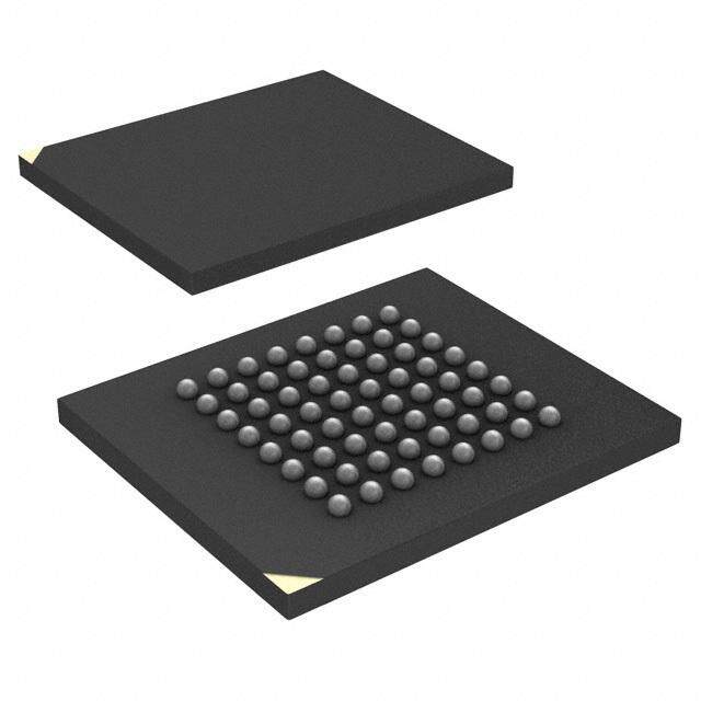
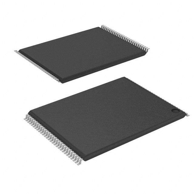
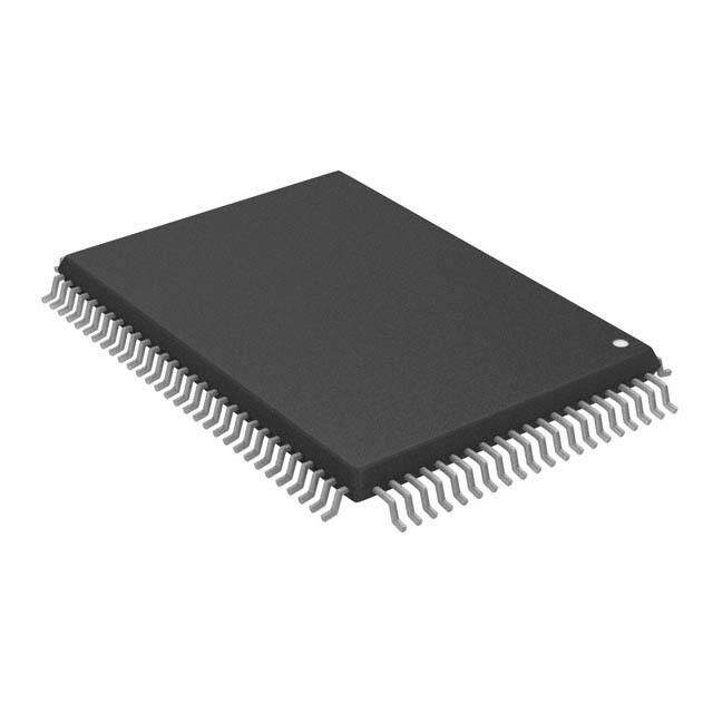
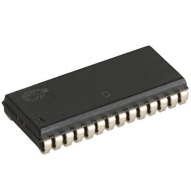
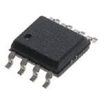
| 产品图片 |
|
| rohs | 符合RoHS无铅 / 符合限制有害物质指令(RoHS)规范要求 |
| 产品系列 | 内存,闪存,Microchip Technology SST25VF010A-33-4C-SAESST25 |
| 数据手册 | http://www.microchip.com/mymicrochip/filehandler.aspx?ddocname=en550392点击此处下载产品Datasheethttp://www.microchip.com/mymicrochip/filehandler.aspx?ddocname=en550325http://www.microchip.com/mymicrochip/filehandler.aspx?ddocname=en556157 |
| 产品型号 | SST25VF010A-33-4C-SAE |
| PCN组件/产地 | http://www.microchip.com/mymicrochip/NotificationDetails.aspx?id=5676&print=view |
| 产品目录页面 | |
| 产品种类 | 闪存 |
| 供应商器件封装 | 8-SOIC |
| 其它名称 | SST25VF010A334CSAE |
| 包装 | 管件 |
| 商标 | Microchip Technology |
| 存储器类型 | FLASH |
| 存储容量 | 1 Mbit |
| 存储类型 | NOR |
| 安装风格 | SMD/SMT |
| 定时类型 | Synchronous |
| 封装 | Tube |
| 封装/外壳 | 8-SOIC(0.154",3.90mm 宽) |
| 封装/箱体 | SOIC-8 |
| 工作温度 | 0°C ~ 70°C |
| 工作温度范围 | 0 C to + 70 C |
| 工厂包装数量 | 100 |
| 接口 | SPI 串行 |
| 接口类型 | SPI |
| 数据总线宽度 | 8 bit |
| 最大工作电流 | 10 mA |
| 最大时钟频率 | 33 MHz |
| 标准包装 | 100 |
| 格式-存储器 | 闪存 |
| 特色产品 | http://www.digikey.com/product-highlights/cn/zh/microchip-sst-serial-parallel-flash-memory/4 |
| 电压-电源 | 2.7 V ~ 3.6 V |
| 电源电压-最大 | 3.6 V |
| 电源电压-最小 | 2.7 V |
| 系列 | SST25VF |
| 组织 | 128 k x 8 |
| 结构 | Sector |
| 访问时间 | 33 ns |
| 速度 | 33 MHz |




- 商务部:美国ITC正式对集成电路等产品启动337调查
- 曝三星4nm工艺存在良率问题 高通将骁龙8 Gen1或转产台积电
- 太阳诱电将投资9.5亿元在常州建新厂生产MLCC 预计2023年完工
- 英特尔发布欧洲新工厂建设计划 深化IDM 2.0 战略
- 台积电先进制程称霸业界 有大客户加持明年业绩稳了
- 达到5530亿美元!SIA预计今年全球半导体销售额将创下新高
- 英特尔拟将自动驾驶子公司Mobileye上市 估值或超500亿美元
- 三星加码芯片和SET,合并消费电子和移动部门,撤换高东真等 CEO
- 三星电子宣布重大人事变动 还合并消费电子和移动部门
- 海关总署:前11个月进口集成电路产品价值2.52万亿元 增长14.8%

PDF Datasheet 数据手册内容提取
1 Mbit SPI Serial Flash SST25VF010A A Microchip Technology Company DataSheet SST's serial flash family features a four-wire, SPI-compatible interface that allows for a low pin-count package occupying less board space and ultimately lowering total system costs. SST25VF010A SPI serial flash memory is manufactured with SST proprietary, high performance CMOS SuperFlash Technology. The split-gate cell design and thick-oxide tunneling injector attain better reliability and manufac- turability compared with alternate approaches. Features (cid:129) Single2.7-3.6VReadandWriteOperations (cid:129) End-of-WriteDetection –SoftwareStatus (cid:129) SerialInterfaceArchitecture –SPICompatible:Mode0andMode3 (cid:129) HoldPin(HOLD#) –Suspendsaserialsequencetothememory (cid:129) 33MHzMaxClockFrequency withoutdeselectingthedevice (cid:129) SuperiorReliability (cid:129) WriteProtection(WP#) –Endurance:100,000Cycles(typical) –Enables/DisablestheLock-Downfunctionofthestatus –Greaterthan100yearsDataRetention register (cid:129) LowPowerConsumption: (cid:129) SoftwareWriteProtection –ActiveReadCurrent:7mA(typical) –WriteprotectionthroughBlock-Protectionbitsinstatus –StandbyCurrent:8µA(typical) register (cid:129) FlexibleEraseCapability (cid:129) TemperatureRange –Uniform4KBytesectors –Commercial:0°Cto+70°C –Uniform32KByteoverlayblocks –Industrial:-40°Cto+85°C –Extended:-20°Cto+85°C (cid:129) FastEraseandByte-Program: (cid:129) PackagesAvailable –Chip-EraseTime:70ms(typical) –Sector-orBlock-EraseTime:18ms(typical) –8-leadSOIC150milbodywidth –Byte-ProgramTime:14µs(typical) –8-contactWSON(5mmx6mm) (cid:129) AutoAddressIncrement(AAI)Programming (cid:129) Allnon-Pb(lead-free)devicesareRoHScompliant –DecreasetotalchipprogrammingtimeoverByte-Pro- gramoperations www.microchip.com ©2011SiliconStorageTechnology,Inc. S725081A 10/11
1 Mbit SPI Serial Flash SST25VF010A A Microchip Technology Company DataSheet Product Description SST’s serial flash family features a four-wire, SPI-compatible interface that allows for a low pin- count package occupying less board space and ultimately lowering total system costs. SST25VF010A SPI serial flash memory is manufactured with SST’s proprietary, high performance CMOS SuperFlash Technology. The split-gate cell design and thick-oxide tunneling injector attain betterreliabilityandmanufacturabilitycomparedwithalternateapproaches. The SST25VF010A device significantly improves performance, while lowering power consumption. The total energy consumed is a function of the applied voltage, current, and time of application. Since for any given voltage range, the SuperFlash technology uses less current to program and has a shorter erase time, the total energy consumed during any Erase or Program operation is less than alternative flash memory technologies. The SST25VF010A device operates with a single 2.7-3.6Vpowersupply. TheSST25VF010Adeviceisofferedinboth8-leadSOICand8-contactWSONpackages.SeeFigure 1forthepinassignments. ©2011SiliconStorageTechnology,Inc. S725081A 10/11 2
1 Mbit SPI Serial Flash SST25VF010A A Microchip Technology Company DataSheet Block Diagram SuperFlash X - Decoder Address Memory Buffers and Latches Y - Decoder I/O Buffers Control Logic and Data Latches Serial Interface 1265B1.0 CE# SCK SI SO WP# HOLD# ©2011SiliconStorageTechnology,Inc. S725081A 10/11 3
1 Mbit SPI Serial Flash SST25VF010A A Microchip Technology Company DataSheet Pin Description CE# 1 8 VDD CE# 1 8 VDD SO 2 7 HOLD# SO 2 7 HOLD# TopView TopView WP# 3 6 SCK WP# 3 6 SCK VSS 4 5 SI VSS 4 5 SI 126508-soicP1.0 126508-wsonP2.0 8-leadSOIC 8-contactWSON Figure 1: Pin Assignments Table 1: Pin Description Symbol PinName Functions SCK SerialClock Toprovidethetimingoftheserialinterface. Commands,addresses,orinputdataarelatchedontherisingedgeoftheclock input,whileoutputdataisshiftedoutonthefallingedgeoftheclockinput. SI SerialData Totransfercommands,addresses,ordataseriallyintothedevice. Input Inputsarelatchedontherisingedgeoftheserialclock. SO SerialData Totransferdataseriallyoutofthedevice. Output Dataisshiftedoutonthefallingedgeoftheserialclock. CE# ChipEnable ThedeviceisenabledbyahightolowtransitiononCE#.CE#mustremainlowfor thedurationofanycommandsequence. WP# WriteProtect TheWriteProtect(WP#)pinisusedtoenable/disableBPLbitinthestatusregis- ter. HOLD# Hold TotemporarilystopserialcommunicationwithSPIflashmemorywithoutresetting thedevice. V PowerSupply Toprovidepowersupply(2.7-3.6V). DD V Ground SS T1.025081 ©2011SiliconStorageTechnology,Inc. S725081A 10/11 4
1 Mbit SPI Serial Flash SST25VF010A A Microchip Technology Company DataSheet Product Identification Table 2: Product Identification Address Data Manufacturer’sID 00000H BFH DeviceID SST25VF010A 00001H 49H T2.025081 Memory Organization The SST25VF010A SuperFlash memory array is organized in 4 KByte sectors with 32 KByte overlay blocks. Device Operation TheSST25VF010AisaccessedthroughtheSPI(SerialPeripheralInterface)buscompatibleprotocol. The SPI bus consist of four control lines; Chip Enable (CE#) is used to select the device, and data is accessedthroughtheSerialDataInput(SI),SerialDataOutput(SO),andSerialClock(SCK). TheSST25VF010AsupportsbothMode0(0,0)andMode3(1,1)ofSPIbusoperations.Thedifference betweenthetwomodes,asshowninFigure2,isthestateoftheSCKsignalwhenthebusmasterisin Stand-bymodeandnodataisbeingtransferred.TheSCKsignalislowforMode0andSCKsignalis highforMode3.Forbothmodes,theSerialDataIn(SI)issampledattherisingedgeoftheSCKclock signalandtheSerialDataOutput(SO)isdrivenafterthefallingedgeoftheSCKclocksignal. CE# MODE3 MODE3 SCK MODE0 MODE0 SI Bit7 Bit6 Bit5 Bit4 Bit3 Bit2 Bit1 Bit0 DONTCARE MSB HIGHIMPEDANCE Bit7 Bit6 Bit5 Bit4 Bit3 Bit2 Bit1 Bit0 SO MSB 1265F02.0 Figure 2: SPI Protocol ©2011SiliconStorageTechnology,Inc. S725081A 10/11 5
1 Mbit SPI Serial Flash SST25VF010A A Microchip Technology Company DataSheet Hold Operation HOLD#pinisusedtopauseaserialsequenceunderwaywiththeSPIflashmemorywithoutresetting the clocking sequence. To activate the HOLD# mode, CE# must be in active low state. The HOLD# modebeginswhentheSCKactivelowstatecoincideswiththefallingedgeoftheHOLD#signal.The HOLDmodeendswhentheHOLD#signal’srisingedgecoincideswiththeSCKactivelowstate. IfthefallingedgeoftheHOLD#signaldoesnotcoincidewiththeSCKactivelowstate,thenthedevice enters Hold mode when the SCK next reaches the active low state. Similarly, if the rising edge of the HOLD# signal does not coincide with the SCK active low state, then the device exits in Hold mode whentheSCKnextreachestheactivelowstate.SeeFigure3forHoldConditionwaveform. OncethedeviceentersHoldmode,SOwillbeinhigh-impedancestatewhileSIandSCKcanbeV orV . IL IH IfCE#isdrivenactivehighduringaHoldcondition,itresetstheinternallogicofthedevice.Aslongas HOLD# signal is low, the memory remains in the Hold condition. To resume communication with the device,HOLD#mustbedrivenactivehigh,andCE#mustbedrivenactivelow.SeeFigure18forHold timing. SCK HOLD# Active Hold Active Hold Active 1265F03.0 Figure 3: Hold Condition Waveform Write Protection The SST25VF010A provides software Write protection. The Write Protect pin (WP#) enables or dis- ables the lock-down function of the status register. The Block-Protection bits (BP1, BP0, and BPL) in thestatusregisterprovideWriteprotectiontothememoryarrayandthestatusregister.SeeTable5for Block-Protectiondescription. Write Protect Pin (WP#) TheWriteProtect(WP#)pinenablesthelock-downfunctionoftheBPLbit(bit7)inthestatusregister. WhenWP#isdrivenlow,theexecutionoftheWrite-Status-Register(WRSR)instructionisdetermined by the value of the BPL bit (see Table 3). When WP# is high, the lock-down function of the BPL bit is disabled. Table 3: Conditions to execute Write-Status-Register (WRSR) Instruction WP# BPL ExecuteWRSRInstruction L 1 NotAllowed L 0 Allowed H X Allowed T3.025081 ©2011SiliconStorageTechnology,Inc. S725081A 10/11 6
1 Mbit SPI Serial Flash SST25VF010A A Microchip Technology Company DataSheet Status Register The software status register provides status on whether the flash memory array is available for any ReadorWriteoperation,whetherthedeviceisWriteenabled,andthestateofthememoryWritepro- tection. During an internal Erase or Program operation, the status register may be read only to deter- mine the completion of an operation in progress. Table 4 describes the function of each bit in the softwarestatusregister. Table 4: Software Status Register Defaultat Bit Name Function Power-up Read/Write 0 BUSY 1=InternalWriteoperationisinprogress 0 R 0=NointernalWriteoperationisinprogress 1 WEL 1=DeviceismemoryWriteenabled 0 R 0=DeviceisnotmemoryWriteenabled 2 BP0 Indicatecurrentlevelofblockwriteprotection(SeeTable5) 1 R/W 3 BP1 Indicatecurrentlevelofblockwriteprotection(SeeTable5) 1 R/W 4:5 RES Reservedforfutureuse 0 N/A 6 AAI AutoAddressIncrementProgrammingstatus 0 R 1=AAIprogrammingmode 0=Byte-Programmode 7 BPL 1=BP1,BP0areread-onlybits 0 R/W 0=BP1,BP0areread/writable T4.0 25081 Busy TheBusybitdetermineswhetherthereisaninternalEraseorProgramoperationinprogress.A“1”for the Busy bit indicates the device is busy with an operation in progress. A “0” indicates the device is readyforthenextvalidoperation. Write Enable Latch (WEL) The Write-Enable-Latch bit indicates the status of the internal memory Write Enable Latch. If the Write-Enable-Latchbitissetto“1”,itindicatesthedeviceisWriteenabled.Ifthebitissetto“0”(reset), it indicates the device is not Write enabled and does not accept any memory Write (Program/Erase) commands.TheWrite-Enable-Latchbitisautomaticallyresetunderthefollowingconditions: (cid:129) Power-up (cid:129) Write-Disable(WRDI)instructioncompletion (cid:129) Byte-Programinstructioncompletion (cid:129) AutoAddressIncrement(AAI)programmingreacheditshighestmemoryaddress (cid:129) Sector-Eraseinstructioncompletion (cid:129) Block-Eraseinstructioncompletion (cid:129) Chip-Eraseinstructioncompletion ©2011SiliconStorageTechnology,Inc. S725081A 10/11 7
1 Mbit SPI Serial Flash SST25VF010A A Microchip Technology Company DataSheet Block Protection (BP1, BP0) TheBlock-Protection(BP1,BP0)bitsdefinethesizeofthememoryarea,asdefinedinTable5,tobe softwareprotectedagainstanymemoryWrite(ProgramorErase)operations.TheWrite-Status-Regis- ter(WRSR)instructionisusedtoprogramtheBP1andBP0bitsaslongasWP#ishighortheBlock- Protect-Lock (BPL) bit is 0. Chip-Erase can only be executed if Block-Protection bits are both 0. After power-up,BP1andBP0aresetto1. Block Protection Lock-Down (BPL) WP# pin driven low (V ), enables the Block-Protection-Lock-Down (BPL) bit. When BPL is set to 1, it IL prevents anyfurtheralterationoftheBPL,BP1,andBP0bits.WhentheWP#pinisdrivenhigh(V ), IH theBPLbithasnoeffectanditsvalueis“Don’tCare”.Afterpower-up,theBPLbitisresetto0. Table 5: Software Status Register Block Protection1 Status RegisterBit Protected ProtectionLevel BP1 BP0 MemoryArea 0 0 0 None 1(1/4MemoryArray) 0 1 018000H-01FFFFH 2(1/2MemoryArray) 1 0 010000H-01FFFFH 3(FullMemoryArray) 1 1 000000H-01FFFFH T5.025081 1. Defaultatpower-upforBP1andBP0is‘11’. Auto Address Increment (AAI) The Auto Address Increment Programming-Status bit provides status on whether the device is in AAI programmingmodeorByte-Programmode.ThedefaultatpowerupisByte-Programmode. ©2011SiliconStorageTechnology,Inc. S725081A 10/11 8
1 Mbit SPI Serial Flash SST25VF010A A Microchip Technology Company DataSheet Instructions Instructions are used to Read, Write (Erase and Program), and configure the SST25VF010A. The instructionbuscyclesare8bitseachforcommands(OpCode),data,andaddresses.Priortoexecut- ing any Byte-Program, Auto Address Increment (AAI) programming, Sector-Erase, Block-Erase, or Chip-Eraseinstructions,theWrite-Enable(WREN)instructionmustbeexecutedfirst.Thecompletelist oftheinstructionsisprovidedinTable6.Allinstructionsaresynchronizedoffahightolowtransitionof CE#.InputswillbeacceptedontherisingedgeofSCKstartingwiththemostsignificantbit.CE#must bedrivenlowbeforeaninstructionisenteredandmustbedrivenhighafterthelastbitoftheinstruction hasbeenshiftedin(exceptforRead,Read-IDandRead-Status-Registerinstructions).Anylowtohigh transitiononCE#,beforereceivingthelastbitofaninstructionbuscycle,willterminatetheinstruction in progressand returnthe device tothe standby mode. Instructioncommands (OpCode), addresses, anddataareallinputfromthemostsignificantbit(MSB)first. Table 6: Device Operation Instructions1 BusCycle2 1 2 3 4 5 6 CycleType/ S S I I Operation3,4 S S S S S S S S S S IN OUT IN OUT IN OUT IN OUT N OUT N OUT Read(20MHz) 03H Hi-Z A23- Hi-Z A15- Hi-Z A7-A0 Hi-Z X DOUT A16 A8 High-Speed-Read(33 0BH Hi-Z A23- Hi-Z A15- Hi-Z A7-A0 Hi-Z X X X DOUT MHz) A16 A8 Sector-Erase5,6 20H Hi-Z A23- Hi-Z A15- Hi-Z A7-A0 Hi-Z - - A16 A8 Block-Erase5,7 52H Hi-Z A23- Hi-Z A15- Hi-Z A7-A0 Hi-Z - - or A16 A8 D8H Chip-Erase6 60H Hi-Z - - - - - - - - or C7H Byte-Program6 02H Hi-Z A23- Hi-Z A15- Hi-Z A7-A0 Hi-Z DIN Hi-Z Hi-Z A16 A8 AutoAddressIncrement AFH Hi-Z A23- Hi-Z A15- Hi-Z A7-A0 Hi-Z DIN Hi-Z Hi-Z (AAI)Program6,8 A16 A8 Read-Status-Register 05H Hi-Z X DOUT - Note - Note - Note9 Note9 (RDSR) 9 9 Enable-Write-Status-Regis- 50H Hi-Z - - - - - - - - ter (EWSR)10 Write-Status-Register 01H Hi-Z Data Hi-Z - - -. - - - (WRSR)10 Write-Enable(WREN) 06H Hi-Z - - - - - - - - Write-Disable(WRDI) 04H Hi-Z - - - - - - - - Read-ID 90H Hi-Z 00H Hi-Z 00H Hi-Z ID Hi-Z X DOUT DOUT1 or Addr11 12 2 ABH T6.025081 1. AMS=MostSignificantAddress AMS=A16forSST25VF010A AddressbitsabovethemostsignificantbitofeachdensitycanbeVILorVIH 2. Onebuscycleiseightclockperiods. 3. Operation:SIN=SerialIn,SOUT=SerialOut 4. X=DummyInputCycles(VILorVIH);-=Non-ApplicableCycles(Cyclesarenotnecessary) 5. Sectoraddresses:useAMS-A12,remainingaddressescanbeVILorVIH ©2011SiliconStorageTechnology,Inc. S725081A 10/11 9
1 Mbit SPI Serial Flash SST25VF010A A Microchip Technology Company DataSheet 6. PriortoanyByte-Program,AAI-Program,Sector-Erase,Block-Erase,orChip-Eraseoperation,theWrite-Enable (WREN)instructionmustbeexecuted. 7. Blockaddressesfor:useAMS-A15,remainingaddressescanbeVILorVIH 8. Tocontinueprogrammingtothenextsequentialaddresslocation,enterthe8-bitcommand,AFH, followedbythedatatobeprogrammed. 9. TheRead-Status-RegisteriscontinuouswithongoingclockcyclesuntilterminatedbyalowtohightransitiononCE#. 10. TheEnable-Write-Status-Register(EWSR)instructionandtheWrite-Status-Register(WRSR)instructionmustworkin conjunctionofeachother.TheWRSRinstructionmustbeexecutedimmediately(verynextbuscycle)aftertheEWSR instructiontomakebothinstructionseffective. 11. Manufacturer’sIDisreadwithA0=0,andDeviceIDisreadwithA0=1.Allotheraddressbitsare00H.TheManufac- turer’sandDeviceIDoutputstreamiscontinuousuntilterminatedbyalowtohightransitiononCE# 12. DeviceID=49HforSST25VF010A Read (20 MHz) The Read instruction outputs the data starting from the specified address location. The data output stream is continuous through all addresses until terminated by a low to high transition on CE#. The internal address pointer will automatically increment until the highest memory address is reached. Once the highest memory address is reached, the address pointer will automatically increment to the beginning(wrap-around)oftheaddressspace,i.e.for4Mbitdensity,oncethedatafromaddressloca- tion7FFFFHhadbeenread,thenextoutputwillbefromaddresslocation00000H. The Read instruction is initiated by executing an 8-bit command, 03H, followed by address bits [A - 23 A ]. CE# must remain active low for the duration of the Read cycle. See Figure 4 for the Read 0 sequence. CE# MODE3 0 1 2 3 4 5 6 7 8 1516 2324 3132 3940 47 48 5556 6364 70 SCK MODE0 03 ADD. ADD. ADD. SI MSB MSB N N+1 N+2 N+3 N+4 HIGHIMPEDANCE SO DOUT DOUT DOUT DOUT DOUT MSB 1265F04.0 Figure 4: Read Sequence ©2011SiliconStorageTechnology,Inc. S725081A 10/11 10
1 Mbit SPI Serial Flash SST25VF010A A Microchip Technology Company DataSheet High-Speed-Read (33 MHz) TheHigh-Speed-Readinstructionsupportingupto33MHzisinitiatedbyexecutingan8-bitcommand, 0BH,followedbyaddressbits[A -A ]andadummybyte.CE#mustremainactivelowfortheduration 23 0 oftheHigh-Speed-Readcycle.SeeFigure5fortheHigh-Speed-Readsequence. Following a dummy byte (8 clocks input dummy cycle), the High-Speed-Read instruction outputs the data starting from the specified address location. The data output stream is continuous through all addresses until terminated by a low to high transition on CE#. The internal address pointer will auto- maticallyincrementuntilthehighestmemoryaddressisreached.Oncethehighestmemoryaddressis reached, the address pointer will automatically increment to the beginning (wrap-around) of the address space, i.e. for 4Mbit density, once the data from address location 07FFFFH has been read, thenextoutputwillbefromaddresslocation000000H. CE# MODE3 0 1 2 3 4 5 6 7 8 1516 23 24 3132 3940 4748 55 56 6364 7172 80 SCK MODE0 SI 0B ADD. ADD. ADD. X MSB MSB N N+1 N+2 N+3 N+4 SO HIGHIMPEDANCE DOUT DOUT DOUT DOUT DOUT MSB Note: X=DummyByte:8ClocksInputDummyCycle(VILorVIH) 1265F05.0 Figure 5: High-Speed-Read Sequence ©2011SiliconStorageTechnology,Inc. S725081A 10/11 11
1 Mbit SPI Serial Flash SST25VF010A A Microchip Technology Company DataSheet Byte-Program TheByte-Programinstructionprogramsthebitsintheselectedbytetothedesireddata.Theselected bytemust beinthe erasedstate(FFH) wheninitiatinga Program operation. AByte-Programinstruction appliedtoaprotectedmemoryareawillbeignored. PriortoanyWriteoperation,theWrite-Enable(WREN)instructionmustbeexecuted.CE#mustremain activelowforthedurationoftheByte-Programinstruction.TheByte-Programinstructionisinitiatedby executingan8-bitcommand,02H,followedbyaddressbits[A -A ].Followingtheaddress,thedatais 23 0 input in order from MSB (bit 7) to LSB (bit 0). CE# must be driven high before the instruction is exe- cuted. The user may poll the Busy bit in the software status register or wait T for the completion of BP theinternalself-timedByte-Programoperation.SeeFigure6fortheByte-Programsequence. CE# MODE3 0 1 2 3 4 5 6 7 8 1516 2324 3132 39 SCK MODE0 SI 02 ADD. ADD. ADD. DIN MSB MSB MSB LSB SO HIGHIMPEDANCE 1265F06.0 Figure 6: Byte-Program Sequence ©2011SiliconStorageTechnology,Inc. S725081A 10/11 12
1 Mbit SPI Serial Flash SST25VF010A A Microchip Technology Company DataSheet Auto Address Increment (AAI) Program The AAI program instruction allows multiple bytes of data to be programmed without re-issuing the nextsequentialaddresslocation.Thisfeaturedecreasestotalprogrammingtimewhentheentiremem- oryarrayistobeprogrammed.AnAAIprograminstructionpointingtoaprotectedmemoryareawillbe ignored.Theselectedaddressrangemustbeintheerasedstate(FFH)wheninitiatinganAAIprogram instruction. Priortoanywriteoperation,theWrite-Enable(WREN)instructionmustbeexecuted.TheAAIprogram instructionisinitiatedbyexecutingan8-bitcommand,AFH,followedbyaddressbits[A -A ].Follow- 23 0 ing the addresses, the data is input sequentially from MSB (bit 7) to LSB (bit 0). CE# must be driven high before the AAI program instruction is executed. The user must poll the BUSY bit in the software statusregisterorwaitT forthecompletionofeachinternalself-timedByte-Programcycle.Oncethe BP device completes programming byte, the next sequential address may be program, enter the 8-bit command, AFH, followed by the data to be programmed. When the last desired byte had been pro- grammed,executetheWrite-Disable(WRDI)instruction,04H,toterminateAAI.Afterexecutionofthe WRDIcommand,theusermustpolltheStatusregistertoensurethedevicecompletesprogramming. SeeFigure7forAAIprogrammingsequence. There is no wrap mode during AAI programming; once the highest unprotected memory address is reached,thedevicewillexitAAIoperationandresettheWrite-Enable-Latchbit(WEL=0). TBP TBP CE# MODE3 0 1 2 3 4 5 6 7 8 1516 2324 313233343536373839 0 1 2 3 4 5 6 7 8 9 101112131415 0 1 SCK MODE0 SI AF A[23:16] A[15:8] A[7:0] DataByte1 AF DataByte2 TBP CE# 0 1 2 3 4 5 6 7 8 9 101112131415 0 1 2 3 4 5 6 7 0 1 2 3 4 5 6 7 8 9 101112131415 SCK SI AF LastDataByte 04 05 WriteDisable(WRDI) ReadStatusRegister(RDSR) Instructiontoterminate Instructiontoverifyendof AAIOperation AAIOperation SO DOUT 1265F07.0 Figure 7: Auto Address Increment (AAI) Program Sequence ©2011SiliconStorageTechnology,Inc. S725081A 10/11 13
1 Mbit SPI Serial Flash SST25VF010A A Microchip Technology Company DataSheet Sector-Erase The Sector-Erase instruction clears all bits in the selected 4 KByte sector to FFH. A Sector-Erase instructionappliedtoaprotectedmemoryareawillbeignored.PriortoanyWriteoperation,theWrite- Enable(WREN)instructionmustbeexecuted.CE#mustremainactivelowforthedurationoftheany commandsequence.TheSector-Eraseinstructionisinitiatedbyexecutingan8-bitcommand,20H,fol- lowed by address bits [A -A ]. Address bits [A -A ] (A =Most Significant address) are used to 23 0 MS 12 MS determinethesectoraddress(SA ),remainingaddressbitscanbeV orV CE#mustbedrivenhigh X IL IH. beforetheinstructionisexecuted.TheusermaypolltheBusybitinthesoftwarestatusregisterorwait T forthecompletionoftheinternalself-timedSector-Erasecycle.SeeFigure8fortheSector-Erase SE sequence. CE# MODE3 0 1 2 3 4 5 6 7 8 1516 2324 31 SCK MODE0 20 ADD. ADD. ADD. SI MSB MSB SO HIGHIMPEDANCE 1265F08.0 Figure 8: Sector-Erase Sequence Block-Erase The Block-Erase instruction clears all bits in the selected 32 KByte block to FFH. A Block-Erase instruction applied to a protected memory area will be ignored. PriortoanyWriteoperation,theWrite- Enable(WREN)instructionmustbeexecuted.CE# must remain active low for the duration of any com- mandsequence.TheBlock-Eraseinstructionisinitiatedbyexecutingan8-bitcommand,52HorD8H, followedbyaddressbits[A -A ].Addressbits[A -A ](A =Mostsignificantaddress)areusedto 23 0 MS 15 MS determineblockaddress(BA ),remainingaddressbitscanbeV orV .CE#mustbedrivenhighbefore X IL IH theinstructionisexecuted.TheusermaypolltheBusybitinthesoftware status register or wait T for the BE completionoftheinternalself-timedBlock-Erasecycle.SeeFigure9fortheBlock-Erasesequence. CE# MODE3 0 1 2 3 4 5 6 7 8 1516 2324 31 SCK MODE0 52orD8 ADD. ADD. ADD. SI MSB MSB SO HIGHIMPEDANCE 1265F09.0 Figure 9: Block-Erase Sequence ©2011SiliconStorageTechnology,Inc. S725081A 10/11 14
1 Mbit SPI Serial Flash SST25VF010A A Microchip Technology Company DataSheet Chip-Erase TheChip-EraseinstructionclearsallbitsinthedevicetoFFH.AChip-Eraseinstructionwillbeignored if any of the memory area is protected. PriortoanyWriteoperation,theWrite-Enable(WREN)instruction mustbeexecuted.CE#mustremainactivelowforthedurationoftheChip-Eraseinstructionsequence. TheChip-Eraseinstructionisinitiatedbyexecutingan8-bitcommand,60HorC7H.CE#mustbedriven highbeforetheinstructionisexecuted.TheusermaypolltheBusybitinthesoftware status register or wait T for the completion of the internal self-timed Chip-Erase cycle. See Figure 10 for the Chip-Erase CE sequence. CE# MODE3 0 1 2 3 4 5 6 7 SCK MODE0 60orC7 SI MSB SO HIGHIMPEDANCE 1265F10.0 Figure 10:Chip-Erase Sequence Read-Status-Register (RDSR) TheRead-Status-Register(RDSR)instructionallowsreadingofthestatusregister.Thestatusregister maybereadatanytimeevenduringaWrite(Program/Erase)operation.WhenaWriteoperationisin progress, the Busy bit may be checked before sending any new commands to assure that the new commandsareproperlyreceivedbythedevice.CE#mustbedrivenlowbeforetheRDSRinstructionis enteredandremainlowuntilthestatusdataisread.Read-Status-Registeriscontinuouswithongoing clock cycles until it is terminated by a low to high transition of the CE#. See Figure 11 for the RDSR instructionsequence. CE# MODE3 0 1 2 3 4 5 6 7 8 9 10 11 12 13 14 SCK MODE0 05 SI MSB HIGHIMPEDANCE Bit7 Bit6 Bit5 Bit4 Bit3 Bit2 Bit1 Bit0 SO MSB Status 1265F11.0 RegisterOut Figure 11:Read-Status-Register (RDSR) Sequence ©2011SiliconStorageTechnology,Inc. S725081A 10/11 15
1 Mbit SPI Serial Flash SST25VF010A A Microchip Technology Company DataSheet Write-Enable (WREN) TheWrite-Enable(WREN)instructionsetstheWrite-Enable-Latchbitto1allowingWriteoperationsto occur. The WREN instruction must be executed prior to any Write (Program/Erase) operation. CE# mustbedrivenhighbeforetheWRENinstructionisexecuted. CE# MODE3 0 1 2 3 4 5 6 7 SCK MODE0 06 SI MSB SO HIGHIMPEDANCE 1265F12.0 Figure 12:Write Enable (WREN) Sequence Write-Disable (WRDI) The Write-Disable (WRDI) instruction resets the Write-Enable-Latch bit and AAI bit to 0 disabling any new Write operations from occurring. CE# must be driven high before the WRDI instruction is exe- cuted. CE# MODE3 0 1 2 3 4 5 6 7 SCK MODE0 04 SI MSB SO HIGHIMPEDANCE 1265F13.0 Figure 13:Write Disable (WRDI) Sequence Enable-Write-Status-Register (EWSR) The Enable-Write-Status-Register (EWSR) instruction arms the Write-Status-Register (WRSR) instruction and opens the status register for alteration. The Enable-Write-Status-Register instruction doesnothaveanyeffectandwillbewasted,ifitisnotfollowedimmediatelybytheWrite-Status-Regis- ter (WRSR) instruction. CE# must be driven low before the EWSR instruction is entered and must be drivenhighbeforetheEWSRinstructionisexecuted. ©2011SiliconStorageTechnology,Inc. S725081A 10/11 16
1 Mbit SPI Serial Flash SST25VF010A A Microchip Technology Company DataSheet Write-Status-Register (WRSR) The Write-Status-Register instruction works in conjunction with the Enable-Write-Status-Register (EWSR)instructiontowritenewvaluestotheBP1,BP0,andBPLbitsofthestatusregister.TheWrite- Status-RegisterinstructionmustbeexecutedimmediatelyaftertheexecutionoftheEnable-Write-Sta- tus-Register instruction (very next instruction bus cycle). This two-step instruction sequence of the EWSR instruction followed by the WRSR instruction works like SDP (software data protection) com- mand structure which prevents any accidental alteration of the status register values. The Write-Sta- tus-Register instruction will be ignored when WP# is low and BPL bit is set to “1”. When the WP# is low, the BPL bit can only be set from “0” to “1” to lock-down the status register, but cannot be reset from“1”to“0”.WhenWP#ishigh,thelock-downfunctionoftheBPLbitisdisabledandtheBPL,BP0, and BP1 bits in the status register can all be changed. As long as BPL bit is set to 0 or WP# pin is driven high (V ) prior to the low-to-high transition of the CE# pin at the end of the WRSR instruction, IH the BP0, BP1, and BPL bit in the status register can all be altered by the WRSR instruction. In this case, a single WRSR instruction can set the BPL bit to “1” to lock down the status register as well as alteringtheBP0andBP1bitatthesametime.SeeTable3forasummarydescriptionofWP#andBPL functions.CE#mustbedrivenlowbeforethecommandsequenceoftheWRSRinstructionisentered anddrivenhighbeforetheWRSRinstructionisexecuted.SeeFigure14forEWSRandWRSRinstruc- tionsequences. CE# MODE3 0 1 2 3 4 5 6 7 MODE3 0 1 2 3 4 5 6 7 8 9 101112131415 SCK MODE0 MODE0 STATUS REGISTERIN 50 01 7 6 5 4 3 2 1 0 SI MSB MSB MSB HIGHIMPEDANCE SO 1265F14.0 Figure 14:Enable-Write-Status-Register (EWSR) and Write-Status-Register (WRSR) Sequence ©2011SiliconStorageTechnology,Inc. S725081A 10/11 17
1 Mbit SPI Serial Flash SST25VF010A A Microchip Technology Company DataSheet Read-ID TheRead-IDinstructionidentifiesthedeviceasSST25VF010AandmanufacturerasSST.Thedevice informationcanbereadfromexecutingan8-bitcommand,90HorABH,followedbyaddressbits[A - 23 A ]. Following the Read-ID instruction, the manufacturer’s ID is located in address 00000H and the 0 deviceIDislocatedinaddress00001H.OncethedeviceisinRead-IDmode,themanufacturer’sand deviceIDoutputdatatogglesbetweenaddress00000Hand00001Huntilterminatedbyalowtohigh transitiononCE#. CE# MODE3 0 1 2 3 4 5 6 7 8 1516 2324 3132 3940 4748 5556 63 SCK MODE0 90orAB 00 00 ADD1 SI MSB MSB HIGH HIGHIMPEDANCE IMPEDANCE SO BF DeviceID BF DeviceID MSB Note: ThemanufacturersanddeviceIDoutputstreamiscontinuousuntilterminatedbyalowtohightransitiononCE#. 1. 00HwilloutputthemanfacturersIDfirstand01HwilloutputdeviceIDfirstbeforetogglingbetweenthetwo. 1265F15.0 Figure 15:Read-ID Sequence ©2011SiliconStorageTechnology,Inc. S725081A 10/11 18
1 Mbit SPI Serial Flash SST25VF010A A Microchip Technology Company DataSheet Electrical Specifications AbsoluteMaximumStressRatings (Applied conditions greater than those listed under “Absolute MaximumStressRatings”maycausepermanentdamagetothedevice.Thisisastressratingonlyand functional operation of the device at these conditions or conditions greater than those defined in the operationalsectionsofthisdatasheetisnotimplied.Exposuretoabsolutemaximumstressratingcon- ditionsmayaffectdevicereliability.) TemperatureUnderBias.............................................. -55°Cto+125°C StorageTemperature................................................. -65°Cto+150°C D.C.VoltageonAnyPintoGroundPotential.............................-0.5VtoV +0.5V DD TransientVoltage(<20ns)onAnyPintoGroundPotential ..................-2.0VtoV +2.0V DD PackagePowerDissipationCapability(T =25°C)................................... 1.0W A SurfaceMountSolderReflowTemperature ........................... 260°Cfor10seconds OutputShortCircuitCurrent1................................................... 50mA 1. Outputshortedfornomorethanonesecond.Nomorethanoneoutputshortedatatime. Table 7: Operating Range Range AmbientTemp V DD Commercial 0°Cto+70°C 2.7-3.6V Industrial -40°Cto+85°C 2.7-3.6V Extended -20°Cto+85°C 2.7-3.6V T7.125081 Table 8: AC Conditions of Test1 InputRise/FallTime OutputLoad 5ns C =30pF L T8.125081 1. SeeFigures20and21 Table 9: DC Operating Characteristics V = 2.7-3.6V DD Limits Symbol Parameter Min Max Units TestConditions I ReadCurrent 10 mA CE#=0.1V /0.9V @20MHz,SO=open DDR DD DD I ProgramandEraseCurrent 30 mA CE#=V DDW DD I StandbyCurrent 15 µA CE#=V ,V =V orV SB DD IN DD SS I InputLeakageCurrent 1 µA V =GNDtoV ,V =V Max LI IN DD DD DD I OutputLeakageCurrent 1 µA V =GNDtoV ,V =V Max LO OUT DD DD DD V InputLowVoltage 0.8 V V =V Min IL DD DD V InputHighVoltage 0.7V V V =V Max IH DD DD DD V OutputLowVoltage 0.2 V I =100µA,V =V Min OL OL DD DD V OutputHighVoltage V -0.2 V I =-100µA,V =V Min OH DD OH DD DD T9.0 25081 ©2011SiliconStorageTechnology,Inc. S725081A 10/11 19
1 Mbit SPI Serial Flash SST25VF010A A Microchip Technology Company DataSheet Table 10:Recommended System Power-up Timings Symbol Parameter Minimum Units T 1 V MintoReadOperation 10 µs PU-READ DD T 1 V MintoWriteOperation 10 µs PU-WRITE DD T10.025081 1. Thisparameterismeasuredonlyforinitialqualificationandafteradesignorprocesschangethatcouldaffectthis parameter. Table 11:Capacitance (TA=25°C,f=1Mhz,otherpinsopen) Parameter Description TestCondition Maximum C 1 OutputPinCapacitance V =0V 12pF OUT OUT C 1 InputCapacitance V =0V 6pF IN IN T11.025081 1. Thisparameterismeasuredonlyforinitialqualificationandafteradesignorprocesschangethatcouldaffectthis parameter. Table 12:Reliability Characteristics Symbol Parameter MinimumSpecification Units TestMethod N 1 Endurance 10,000 Cycles JEDECStandardA117 END T 1 DataRetention 100 Years JEDECStandardA103 DR I 1 LatchUp 100+I mA JEDECStandard78 LTH DD T12.025081 1. Thisparameterismeasuredonlyforinitialqualificationandafteradesignorprocesschangethatcouldaffectthis parameter. ©2011SiliconStorageTechnology,Inc. S725081A 10/11 20
1 Mbit SPI Serial Flash SST25VF010A A Microchip Technology Company DataSheet Table 13:AC Operating Characteristics V = 2.7-3.6V DD Limits 20MHz 33MHz Symbol Parameter Min Max Min Max Units F SerialClockFrequency 20 33 MHz CLK T SerialClockHighTime 20 13 ns SCKH T SerialClockLowTime 20 13 ns SCKL T 1 SerialClockRiseTime(slewrate) 0.1 0.1 V/ns SCKR T 1 SerialClockFallTime(slewrate) 0.1 0.1 V/ns SCKF T 2 CE#ActiveSetupTime 20 12 ns CES T 2 CE#ActiveHoldTime 20 12 ns CEH T 2 CE#NotActiveSetupTime 10 10 ns CHS T 2 CE#NotActiveHoldTime 10 10 ns CHH T CE#HighTime 100 100 ns CPH T CE#HightoHigh-ZOutput 20 14 ns CHZ T SCKLowtoLow-ZOutput 0 0 ns CLZ T DataInSetupTime 5 3 ns DS T DataInHoldTime 5 3 ns DH T HOLD#LowSetupTime 10 10 ns HLS T HOLD#HighSetupTime 10 10 ns HHS T HOLD#LowHoldTime 15 10 ns HLH T HOLD#HighHoldTime 10 10 ns HHH T HOLD#LowtoHigh-ZOutput 20 14 ns HZ T HOLD#HightoLow-ZOutput 20 14 ns LZ T OutputHoldfromSCKChange 0 0 ns OH T OutputValidfromSCK 20 12 ns V T Sector-Erase 25 25 ms SE T Block-Erase 25 25 ms BE T Chip-Erase 100 100 ms SCE T Byte-Program 20 20 µs BP T13.025081 1. MaximumSerialClockRiseandFalltimesmaybelimitedbyTSCKHandTSCKLrequirements. 2. RelativetoSCK. ©2011SiliconStorageTechnology,Inc. S725081A 10/11 21
1 Mbit SPI Serial Flash SST25VF010A A Microchip Technology Company DataSheet TCPH CE# TCHH TCEH TCHS TSCKF TCES SCK TDS TDH TSCKR MSB LSB SI SO HIGH-Z HIGH-Z 1265F16.0 Figure 16:Serial Input Timing Diagram CE# TSCKH TSCKL SCK TOH TCLZ TCHZ SO MSB LSB TV SI 1265F17.0 Figure 17:Serial Output Timing Diagram CE# THHH THLS THHS SCK THLH THZ TLZ SO SI HOLD# 1265F18.0 Figure 18:Hold Timing Diagram ©2011SiliconStorageTechnology,Inc. S725081A 10/11 22
1 Mbit SPI Serial Flash SST25VF010A A Microchip Technology Company DataSheet VDD VDDMax Chipselectionisnotallowed. Allcommandsarerejectedbythedevice. VDDMin TPU-READ Devicefully accessible TPU-WRITE Time 1265F19.0 Figure 19:Power-up Timing Diagram ©2011SiliconStorageTechnology,Inc. S725081A 10/11 23
1 Mbit SPI Serial Flash SST25VF010A A Microchip Technology Company DataSheet VIHT VHT VHT INPUT REFERENCEPOINTS OUTPUT VLT VLT VILT 1265F20.0 ACtestinputsaredrivenatV (0.9V )foralogic“1”andV (0.1V )foralogic“0”.Mea- IHT DD ILT DD surement reference points for inputs and outputs are V (0.7V ) and V (0.3V ). Input HT DD LT DD riseandfalltimes(10%90%)are<5ns. Note: VHT-VHIGHTest VLT-VLOWTest VIHT-VINPUTHIGHTest VILT-VINPUTLOWTest Figure 20:AC Input/Output Reference Waveforms TOTESTER TODUT CL 1265F21.0 Figure 21:A Test Load Example ©2011SiliconStorageTechnology,Inc. S725081A 10/11 24
1 Mbit SPI Serial Flash SST25VF010A A Microchip Technology Company DataSheet Product Ordering Information SST 25 VF 010A - 33 - 4I - QAE XX XX XXXX - XX - XX - XXX EnvironmentalAttribute E1=non-Pb PackageModifier A=8leadsorcontacts PackageType S=SOIC Q=WSON TemperatureRange C=Commercial=0°Cto+70°C I=Industrial=-40°Cto+85°C E=Extended=-20°Cto+85°C MinimumEndurance 4=10,000cycles OperatingFrequency 33=33MHz DeviceDensity 010=1Mbit Voltage V=2.7-3.6V ProductSeries 25=SerialPeripheralInterface flashmemory 1. Environmentalsuffix“E”denotesnon-Pbsol- der.SSTnon-Pbsolderdevicesare“RoHS Compliant”. Valid combinations for SST25VF010A SST25VF010A-33-4C-SAE SST25VF010A-33-4C-QAE SST25VF010A-33-4I-SAE SST25VF010A-33-4I-QAE SST25VF010A-33-4E-SAE SST25VF010A-33-4E-QAE Note:Validcombinationsarethoseproductsinmassproductionorwillbeinmassproduction.ConsultyourSST salesrepresentativetoconfirmavailabilityofvalidcombinationsandtodetermineavailabilityofnewcombi- nations. ©2011SiliconStorageTechnology,Inc. S725081A 10/11 25
1 Mbit SPI Serial Flash SST25VF010A A Microchip Technology Company DataSheet Packaging Diagrams Pin#1 Identifier TOPVIEW SIDEVIEW 7° 4places 0.51 5.0 0.33 4.8 1.27BSC ENDVIEW 45° 7° 0.25 4places 0.10 4.00 3.80 1.75 6.20 1.35 0.25 0° 5.80 0.19 8° 1.27 Note: 1.ComplieswithJEDECpublication95MS-012AAdimensions, 0.40 althoughsomedimensionsmaybemorestringent. 08-soic-5x6-SA-8 2.Alllineardimensionsareinmillimeters(max/min). 3.Coplanarity:0.1mm 4.Maximumallowablemoldflashis0.15mmatthepackageendsand0.25mmbetweenleads. 1mm Figure 22:8-leadSmallOutlineIntegratedCircuit(SOIC)150milbodywidth(4.9mmx6mm) SST Package Code: SA ©2011SiliconStorageTechnology,Inc. S725081A 10/11 26
1 Mbit SPI Serial Flash SST25VF010A A Microchip Technology Company DataSheet TOPVIEW SIDEVIEW BOTTOMVIEW Pin#1 0.2 Pin#1 Corner 1.27BSC 5.00±0.10 0.076 4.0 0.48 0.35 3.4 0.70 0.05Max 0.50 6.00± 0.10 0.80 0.70 CROSSSECTION Note: 1.Alllineardimensionsareinmillimeters(max/min). 2.Untoleranceddimensions(shownwithboxsurround) arenominaltargetdimensions. 0.80 3.Theexternalpaddleiselectricallyconnectedtothe 0.70 dieback-sideandpossiblytocertainVSSleads. 1mm ThispaddlecanbesolderedtothePCboard; itissuggestedtoconnectthispaddletotheVSSoftheunit. 8-wson-5x6-QA-9.0 Connectionofthispaddletoanyothervoltagepotentialcan resultinshortsand/orelectricalmalfunctionofthedevice. Figure 23:8-contact Very-very-thin Small Outline No-lead (WSON) SST Package Code: QA ©2011SiliconStorageTechnology,Inc. S725081A 10/11 27
1 Mbit SPI Serial Flash SST25VF010A A Microchip Technology Company DataSheet Table 14:Revision History Revisions Description Date 00 (cid:129) Initialrelease Jun2004 01 (cid:129) AddedRoHScomplianceinformationonpage1andinthe“Product Jan2005 OrderingInformation”onpage25 (cid:129) Updatedthesurfacemountleadtemperaturefrom240°Cto260°Cand thetimefrom3secondsto10secondsonpage19. (cid:129) UpdatedTable13onpage21toincludetheparametersT and SCKR T SCKF 02 (cid:129) UpdatedQApackagedrawingtoversion9 Jan2006 (cid:129) MigrateddocumenttoaDataSheet (cid:129) UpdatedSurfaceMountSolderReflowTemperatureinformation (cid:129) Removedleadedpartnumbers A (cid:129) Appliednewdocumentformat Oct2011 (cid:129) Releaseddocumentunderletterrevisionsystem (cid:129) UpdatedSpecnumberfromS71265toDS25081 ISBN:978-1-61341-695-2 ©2011SiliconStorageTechnology,Inc–aMicrochipTechnologyCompany.Allrightsreserved. SST,SiliconStorageTechnology,theSSTlogo,SuperFlash,MTP,andFlashFlexareregisteredtrademarksofSiliconStorageTech- nology,Inc.MPF,SQI,SerialQuadI/O,andZ-ScalearetrademarksofSiliconStorageTechnology,Inc.Allothertrademarksand registeredtrademarksmentionedhereinarethepropertyoftheirrespectiveowners. Specificationsaresubjecttochangewithoutnotice.Refertowww.microchip.comforthemostrecentdocumentation.Forthemostcurrent packagedrawings,pleaseseethePackagingSpecificationlocatedathttp://www.microchip.com/packaging. Memorysizesdenoterawstoragecapacity;actualusablecapacitymaybeless. SSTmakesnowarrantyfortheuseofitsproductsotherthanthoseexpresslycontainedintheStandardTermsandConditionsof Sale. Forsalesofficelocationsandinformation,pleaseseewww.microchip.com. SiliconStorageTechnology,Inc. AMicrochipTechnologyCompany www.microchip.com ©2011SiliconStorageTechnology,Inc. S725081A 10/11 28
Mouser Electronics Authorized Distributor Click to View Pricing, Inventory, Delivery & Lifecycle Information: M icrochip: SST25VF010A-33-4C-QAE SST25VF010A-33-4C-SAE SST25VF010A-33-4I-SAE SST25VF010A-33-4I-QAE SST25VF010A-33-4C-QAE-T SST25VF010A-33-4I-QAE-T SST25VF010A-33-4I-ZAE
 Datasheet下载


