ICGOO在线商城 > 射频/IF 和 RFID > RF 放大器 > SST12LP08-QX6E
 Datasheet下载
- 型号: SST12LP08-QX6E
- 制造商: Microchip
- 库位|库存: xxxx|xxxx
- 要求:
| 数量阶梯 | 香港交货 | 国内含税 |
| +xxxx | $xxxx | ¥xxxx |
查看当月历史价格
查看今年历史价格
SST12LP08-QX6E产品简介:
ICGOO电子元器件商城为您提供SST12LP08-QX6E由Microchip设计生产,在icgoo商城现货销售,并且可以通过原厂、代理商等渠道进行代购。 SST12LP08-QX6E价格参考¥询价-¥询价。MicrochipSST12LP08-QX6E封装/规格:RF 放大器, 射频放大器 IC 802.11b/g/n 2.4GHz ~ 2.5GHz 6-XSON(1.5x1.5)。您可以下载SST12LP08-QX6E参考资料、Datasheet数据手册功能说明书,资料中有SST12LP08-QX6E 详细功能的应用电路图电压和使用方法及教程。
SST12LP08-QX6E 是由 Microchip Technology 提供的一款 RF(射频)放大器,广泛应用于无线通信、雷达系统、卫星通信和测试测量设备等领域。以下是该型号可能的应用场景:

 1. 无线通信
   - 蜂窝基站:用于增强信号功率,确保基站与移动设备之间的可靠通信。
   - Wi-Fi 和蓝牙模块:提高无线信号的传输距离和稳定性。
   - 物联网 (IoT) 设备:在低功耗环境下提供高效的信号放大功能,支持远程传感器数据传输。

 2. 雷达系统
   - 汽车雷达:应用于自动驾驶辅助系统(ADAS),如盲点监测、碰撞预警等,提升信号灵敏度和探测范围。
   - 气象雷达:用于天气预报和灾害预警,放大射频信号以检测更远距离的气象目标。

 3. 卫星通信
   - 地面站设备:放大上行链路信号,确保卫星接收到清晰的指令信息。
   - 卫星终端:在便携式卫星通信设备中使用,实现高质量的语音和数据传输。

 4. 测试与测量
   - 信号发生器:为实验室设备提供稳定的高功率射频信号源。
   - 频谱分析仪:增强微弱信号的检测能力,帮助工程师分析复杂的射频环境。

 5. 工业自动化
   - 无线传感器网络:在工厂或远程监控系统中,放大传感器采集的数据信号,确保实时传输。
   - 射频识别 (RFID):提高读写器的发射功率,扩大识别范围。

 6. 医疗设备
   - 无线健康监测设备:例如可穿戴心率监测器或血糖仪,通过高效射频放大器将数据发送至手机或云端。
   - 超声波成像系统:用于信号处理阶段,改善图像分辨率和深度。

SST12LP08-QX6E 的设计注重高线性度、低噪声和高效率,使其能够满足多种高频应用场景的需求。同时,其紧凑型封装也适合对空间要求严格的现代电子设备。
| 参数 | 数值 |
| 产品目录 | |
| 描述 | IC RF PWR AMP 802.11B/G/N 6-QFN |
| 产品分类 | |
| 品牌 | Microchip Technology |
| 数据手册 | 点击此处下载产品Datasheethttp://www.microchip.com/mymicrochip/filehandler.aspx?ddocname=en555159http://www.microchip.com/mymicrochip/filehandler.aspx?ddocname=en559476 |
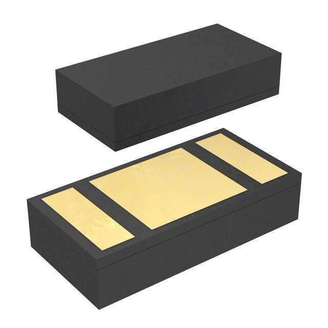
| 产品图片 |
|
| P1dB | - |
| 产品型号 | SST12LP08-QX6E |
| RF类型 | 802.11b/g/n |
| rohs | 无铅 / 符合限制有害物质指令(RoHS)规范要求 |
| 产品系列 | - |
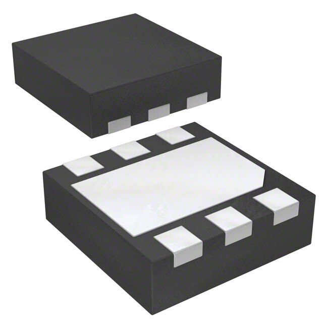
| 供应商器件封装 | 6-XSON(1.5x1.5) |
| 其它名称 | SST12LP08-QX6ECT |
| 包装 | 剪切带 (CT) |
| 噪声系数 | - |
| 增益 | 30dB |
| 封装/外壳 | 6-XFDFN 裸露焊盘 |
| 标准包装 | 1 |
| 测试频率 | - |
| 电压-电源 | 3 V ~ 3.6 V |
| 电流-电源 | 200mA |
| 频率 | 2.4GHz ~ 2.5GHz |


- 商务部:美国ITC正式对集成电路等产品启动337调查
- 曝三星4nm工艺存在良率问题 高通将骁龙8 Gen1或转产台积电
- 太阳诱电将投资9.5亿元在常州建新厂生产MLCC 预计2023年完工
- 英特尔发布欧洲新工厂建设计划 深化IDM 2.0 战略
- 台积电先进制程称霸业界 有大客户加持明年业绩稳了
- 达到5530亿美元!SIA预计今年全球半导体销售额将创下新高
- 英特尔拟将自动驾驶子公司Mobileye上市 估值或超500亿美元
- 三星加码芯片和SET,合并消费电子和移动部门,撤换高东真等 CEO
- 三星电子宣布重大人事变动 还合并消费电子和移动部门
- 海关总署:前11个月进口集成电路产品价值2.52万亿元 增长14.8%


PDF Datasheet 数据手册内容提取
D 2.4 GHz High-Power, High-Gain Power Amplifier N SST12LP08 A Microchip Technology Company DataSheet A L The SST12LP08 is a versatile power amplifier based on the highly-reliable InGaP/ GaAs HBT technology. Easily configured for linear high-power applications with A excellent power-added efficiency while operating over the 2.4- 2.5 GHz frequency band, it typically provides 30 dB gain withY 34% power-added efficiency, while meeting 802.11b/g spectrum mask at 23.5 dBm. The SST12LP08 also features easy board-level usage along with high-speed power-up/down control through a I single combined reference voltage pin and is offered in both 12-contact XQFN R and 6-contact XSON packages. T Features N A (cid:129) HighGain: (cid:129) LowShut-downCurrent(~2µA) –Typically30dBgainacross2.4~2.5GHzovertempera- (cid:129) Hightemperaturestability ture0°Cto+85°C T –~1EdBgain/powervariationbetween0°Cto+85°C (cid:129) Highlinearoutputpower: (cid:129) ExcellentOn-chippowerdetection –>28dBmP1dB -Pleasereferto“AbsoluteMaximumStressRatings”on page6 E (cid:129) 20dBdynamicrangeon-chippowerdetection –Meets802.11gOFDMACPRrequirementupto23.5 D dBm (cid:129) Simpleinput/outputmatching –~3%addedEVMupto20dBmfor 54Mbps802.11gsignal (cid:129) Packagesavailable –Meets802.11bACPRrequiremIentupto23.5dBm –12-contactXQFN–2mmx2mm –6-contactXSON–1.5mmx1.5mm (cid:129) Highpower-addedefficiencRy/Lowoperatingcur- I rentforboth802.11g/bapplications (cid:129) Allnon-Pb(lead-free)devicesareRoHScompliant –~34%/200mA@P =23.5dBmfor802.11b/g F OUT (cid:129) Single-pinlowI power-up/downcontrol REF –I <2mA Applications REF P (cid:129) Lowidlecurrent N (cid:129) WLAN(IEEE802.11b/g/n) –~85mAI for12-contactXQFN CQ –~65mAICQfor6-contactXSON (cid:129) HomeRF (cid:129) High-speedpoOwer-up/down (cid:129) Cordlessphones –Turnon/offtime(10%-90%)<100ns O –Typicalpower-up/downdelaywithdriverdelayincluded (cid:129) 2.4GHzISMwirelessequipment <200ns R C P www.microchip.com ©2012SiliconStorageTechnology,Inc. DS75073B 06/12
D 2.4 GHz High-Power, High-Gain Power Amplifier N SST12LP08 A Microchip Technology Company DataSheet A Product Description L TheSST12LP08isaversatilepoweramplifierbasedonthehighly-reliableInGaP/GaAsHBTtechnology. The SST12LP08 can be easily configured for h igh-power applications witAh good power-added effi- ciencywhileoperatingoverthe2.4-2.5GHzfrequencyband.Ittypicallyprovides30dBgainwith34% Y power-addedefficiency(PAE)@POUT=23.5dBmfor802.11b/g. The SST12LP08 has excellent linearity, typically ~3% added EVM at 20 dBm output power which is I essentialfor54Mbps802.11goperationwhilemeeting802.11gspectrummaskat23.5dBm. R T TheSST12LP08canalsobeeasilyconfiguredforhigh-efficiencyoperation,typically~3%addedEVM at18dBmoutputpowerand95mAtotalpowerconsumptionfor54Mbps802.11gapplications.High- efficiency operation is desirable in embedded applications, such as in hand-held units, where SST12LP08canprovide30dBgainandmeet802.11b/gspectrummaskat22dBmoutputpowerwith N A 34%PAE. The SST12LP08 also features easy board-level usage along with high-speed power-up/down control throughasinglecombinedreTferencevoltagepin.Ultra-lowreferencecurrent(totalIREF~2mA)makes theSST12LP08controllablebyanon/offswitchingsigEnaldirectlyfromthebasebandchip.Thesefea- tures coupled with low operating current make the SST12LP08 ideal for the final stage power amplifi- cationinbattery-powered802.11b/g/nWLANtransmitterapplications. E The SST12LP08 has an excellent on-chip, single-ended power detector, which features wide-range D (>15 dB) with dB-wise linearization. The excellent on-chip power detector provides a reliable solution toboard-levelpowercontrol. TheSST12LP08Iis offered in both 12-contact XQFN and 6-contact XSON packages. See Figure 3 for pinassignmentsandTables1and2forpindescriptions. R I F P N O O R C P ©2012SiliconStorageTechnology,Inc. DS75073B 06/12 2
D 2.4 GHz High-Power, High-Gain Power Amplifier N SST12LP08 A Microchip Technology Company DataSheet A Functional Blocks L 1 A C C YC C N V N 12 11 10 I R T NC 1 9 NC N RFIN 2A 8 RFOUT/VCC2 NC 3 7 NC T BiasCircuit E 4 5 6 E D V V D C R E C E T b F I 1399B1.0 Figure 1: FRunctional Block DiagramI12-Contact XQFN (QXB) F P VCNC1 1 6 VCC2/RFOUT O RFIN 2 5 DET O R VCCb 3 Bias Circuit 4 VREF C 1399F13.0 Figure 2: Functional Block Diagram 6-Contact XSON (QX6) P ©2012SiliconStorageTechnology,Inc. DS75073B 06/12 3
D 2.4 GHz High-Power, High-Gain Power Amplifier N SST12LP08 A Microchip Technology Company DataSheet A Pin Assignments L 1 A C C C C N YV N 12 11 10 I R T NC 1 9 NC TopView RFIN 2 A N8 RFOUT/VCC2 (Contacts facing down) NC 3 7 NC T E 4 5 6 E V VDD C R E C E T b F I 1399P1.0 R 12I-ContactXQFN F P N VCC1 1 6 VCC2/RFOUT O Top View ORFIN 2 5 DET (Contacts facing down) RF & DC R VCCb 3 Ground 4 VREF 0 C 1399 F14.1 P 6-ContactXSON Figure 3: Pin Assignments ©2012SiliconStorageTechnology,Inc. DS75073B 06/12 4
D 2.4 GHz High-Power, High-Gain Power Amplifier N SST12LP08 A Microchip Technology Company DataSheet A Pin Descriptions L Table 1: Pin Description for12-Contact XQFN (QXB) A Symbol PinNo. PinName Type1 Function GND 0 Ground YLow-inductanceGNDpad NC 1 NoConnection Unconnectedpin RFIN 2 I RFinput,DCdeIcoupled NC 3 NoConnection R Unconnectedpin T VCCb 4 PowerSupply PWR Supplyvoltageforbiascircuit VREF 5 PWR 1stand2ndstageidlecurrentcontrol DET 6 O On-chippowerdetector N NC 7 NoConnAection Unconnectedpin VCC2/ 8 PowerSupply PWR/O PowerSupply,2ndstage/RFoutput RFOUT NC 9 NoTConnection Unconnectedpin NC 10 NoConnection EUnconnectedpin VCC1 11 PowerSupply PWR Powersupply,1ststage NC 12 NoConnection Unconnectedpin E T1.0 75073 1. I=Input,O=Output D Table 2: Pin Description, 6-contact XSON (QX6) I Symbol PinNo. PinName Type1 Function R I GND 0 Ground LowinductanceGNDpad V 1 PowerSupplyFPWR Powersupply,1ststage CC1 RF 2 I RFinput,DCdecoupled IN V 3 PowerSupply PWR Supplyvoltageforbiascircuit CCbP VREF 4 N PWR 1stand2ndstageidlecurrentcontrol Det 5 O On-chippowerdetector V /RFOUT 6 PowerSupply PWR/O Powersupply,2ndstage/RFOutput CC2 O T2.0 75073 1. I=Input,O=Output O R C P ©2012SiliconStorageTechnology,Inc. DS75073B 06/12 5
D 2.4 GHz High-Power, High-Gain Power Amplifier N SST12LP08 A Microchip Technology Company DataSheet A Electrical Specifications L TheACandDCspecificationsforthepoweramplifierinterfacesignals.RefertoTable4fortheDCvoltageand currentspecifications.RefertoFigures4through11fortheRFperformance. A AbsoluteMaximumStressRatings (AppliedYconditions greater than those listed under “Absolute MaximumStressRatings”maycausepermanentdamagetothedevice.Thisisastressratingonlyand functional operation of the device at these conditions or conditions greater than those defined in the I operationalsectionsofthisdatasheetisnotimplied.Exposuretoabsolutemaximumstressratingcon- ditionsmayaffectdevicereliability.) R T Inputpowertopin2(P )..................................................... +5dBm IN Averageoutputpower(P )1................................................ +26dBm OUT SupplyVoltageatpins4,8,and11(V )for12-contactXQFN..................-0.3Vto+5.0V ACC N SupplyVoltageatpins1,3,and6(V )for6-contactXSON....................-0.3Vto+5.0V CC Referencevoltagetopin5(V )or12-contactXQFN.........................-0.3Vto+3.3V REF Referencevoltagetopin4(V )for6-contactXSON.........................-0.3Vto+3.3V TREF DCsupplycurrent(ICC)2 .......................E.............................. 400mA OperatingTemperature(T ) ............................................ -40ºCto+85ºC A StorageTemperature(T )........................................... -40ºCto+120ºC STG E MaximumJunctionTemperature(T ) ........................................... +150ºC J D SurfaceMountSolderReflowTemperature ........................... 260°Cfor10seconds 1. NevermeasurewithCWsource.Pulsedsingle-tonesourcewith<50%dutycycleisrecommended.Exceedingthemax- imumratingofaverageoutputpowercouldcausepermanentdamagetothedevice. 2. MeasuredwiIth100%dutycycle54Mbps802.11gOFDMSignal R I Table 3: Operating Range F Range AmbientTemp V CC Industrial -40°Cto+85°C 3.3V P T3.075073 N O O R C P ©2012SiliconStorageTechnology,Inc. DS75073B 06/12 6
D 2.4 GHz High-Power, High-Gain Power Amplifier N SST12LP08 A Microchip Technology Company DataSheet A Table 4: DC Electrical Characteristics at 25°C L Symbol Parameter Min. Typ Max. Unit TestConditions SupplyVoltageatpins4,8,11for12-contactXQFN 2.75 3.3 4.2 V Figure12 V CC SupplyVoltageatpins1,3,6for6-contact XSON 2.75 3.3 A4.2 V Figures13and14 Idlecurrentfor802.11gtomeetEVM~3%@20dBmfor 85 mA Figure12 Y 12-contactXQFN Idlecurrentfor802.11gtomeetEVM~3%@20dBmfor 65 mA Figure13 I CQ 6-contactXSON I Idlecurrentfor802.11gtomeetEVRM~3%@18dBmfor 48 mA Figure14 T 6-contactXSON Currentconsumptionfor802.11gtomeetEVM~3%@ 148 mA Figure12 20dBmfor12-contactXQFN I Currentconsumptionfor802.11gtomeetEVM~3%@ N140 mA Figure13 CC A (802.11g) 20dBmfor6-contactXSON CurrentConsumptionfor802.11gtomeetEVM~3%@ 95 mA Figure14 18dBmfor6-contactXSON T Currentconsumptionfor802.11b/g,23.5dBmfor 200 mA Figure12 E 12-contactXQFN ICC Currentconsumptionfor802.11b/g,23.5dBmfor 200 mA Figure13 (802.11b/g) 6-contactXSEON CurrentConsumptionfor802.11b/g,22dDBmfor 140 mA Figure14 6-contactXSON ReferenceVoltagefor12-contactXQFNwith75resistor 2.75 2.85 2.95 V Figure12 V RefereInceVoltagefor6-contactXSONwith180resistor 2.75 2.85 2.95 V Figure13 REG ReferenceVoltagefor6-contactXSONwith390resistor 2.75 2.85 2.95 V Figure14 R I T4.2 75073 F Table 5: AC Electrical Characteristics for Configuration at 25°C SymbPol Parameter Min. Typ Max. Unit N F Frequencyrange 2412 2484 MHz L-U G Smallsignalgain 29 30 dB G Gainvariationoverband(2412–2484MHz) ±0.5 dB VAR1 O G Gainrippleoverchannel(20MHz) 0.2 dB VAR2 O ACPR Meet11bspectrummask 23 dBm Meet11gOFDM54Mbpsspectrummask 23 dBm AddedEVM @20dBmoutputwith11gOFDM54Mbpssignal 3 % R 2f,3f,4f,5f Harmonicsat22dBm,withoutexternalfilters -40 dBc C T5.2 75073 P ©2012SiliconStorageTechnology,Inc. DS75073B 06/12 7
D 2.4 GHz High-Power, High-Gain Power Amplifier N SST12LP08 A Microchip Technology Company DataSheet A Typical Performance Characteristics L Test Conditions: V = 3.3V, T = 25°C, unless otherwise noted CC A A Y S11versusFrequency S12versusFrequency 0 0 I -10 -5 R T -20 -10 S11(dB) -15 S12(dB) --4300 N A -50 -20 -60 -25 -70 T -30 -80 E 0.0 1.0 2.0 3.0 4.0 5.0 6.0 7.0 0.0 1.0 2.0 3.0 4.0 5.0 6.0 7.0 Frequency(GHz) Frequency(GHz) E S21versusFrequency D S22versusFrequency 40 0 30 I -5 20 R I-10 dB) 10 B) 1( 0 F (d -15 S2 22 S -10 -20 -20 P -25 -30 N -40 -30 0.0 1.0 2.0 3.0 4.0 5.0 6.0 7.0 0.0 1.0 2.0 3.0 4.0 5.0 6.0 7.0 Frequency(GHz) Frequency(GHz) O O 1399S-Parms.1.1 Figure 4: S-Parameters R C P ©2012SiliconStorageTechnology,Inc. DS75073B 06/12 8
D 2.4 GHz High-Power, High-Gain Power Amplifier N SST12LP08 A Microchip Technology Company DataSheet A Typical Performance Characteristics L TestConditions:V =3.3V,T =25°C,54Mbps802.11gOFDMSignal,equalizer CC A training using sequence plus data A Y EVM versus Output Power I 10 R T 9 Freq=2.412 GHz 8 Freq=2.442 GHz 7 Freq=2.472 GHz N A ) 6 % ( M 5 V E 4 T E 3 2 E 1 D 0 9 10 11 12 13 14 15 16 17 18 19 20 21 22 23 I Output Power (dBm) 1391 F4.1 Figure5: ERVMversusOutputPoweIrmeasuredwith“sequenceplusdata”channelestimation F Power Gain versus Output Power P 40 N 38 Freq=2.412 GHz 36 Freq=2.442 GHz O B) 34 OFreq=2.472 GHz d n ( 32 ai G 30 R er 28 w o C P 26 24 P 22 20 9 10 11 12 13 14 15 16 17 18 19 20 21 22 23 Output Power (dBm) 1391 F5.1 Figure 6: Power Gain versus Output Power ©2012SiliconStorageTechnology,Inc. DS75073B 06/12 9
D 2.4 GHz High-Power, High-Gain Power Amplifier N SST12LP08 A Microchip Technology Company DataSheet A L Supply Current versus Output Power A 200 190 Y Freq=2.412 GHz 180 Freq=2.442 GHz A) 170 Freq=2.472 GHz I m ( 160 R t T n 150 e r r 140 u C 130 y pl 120 A N p u 110 S 100 T 90 E 80 9 10 11 12 13 14 15 16 17 18 19 20 21 22 23 E Output Power (dBm) D 1391 F6.1 Figure 7: Total Current Consumption for 802.11g operation versus Output Power I R I PAFE versus Output Power 30 28 P Freq=2.412 GHz 26 N Freq=2.442 GHz 24 22 Freq=2.472 GHz 20 O ) 18 % ( 16 O E A 14 P 12 10 R 8 6 C 4 2 0 P 9 10 11 12 13 14 15 16 17 18 19 20 21 22 23 Output Power (dBm) 1391 F7.1 Figure 8: PAE versus Output Power ©2012SiliconStorageTechnology,Inc. DS75073B 06/12 10
D 2.4 GHz High-Power, High-Gain Power Amplifier N SST12LP08 A Microchip Technology Company DataSheet A L Detector Voltage versus Output Power A 1.8 Y 1.7 Freq=2.412 GHz 1.6 ) Freq=2.442 GHz V 1.5 I e ( Freq=2.472 GHz g 1.4 R a T t 1.3 ol V 1.2 r o 1.1 t ec 1.0 A N t e 0.9 D 0.8 0.7 T 0.6 E 0.5 0 1 2 3 4 5 6 7 8 9 10 11 12 13 14 15 16 17 18 19 20 21 22 23 24 25 E Output Power (dBm) D 1391 F8.3 Figure 9: Detector Characteristics versus Output Power I R I 10 F Freq=2.412GHZ 0 Freq=2.442GHz P -10 N Freq=2.472GHz ) B -20 d O( e d u -30 O t pli m -40 A R -50 C -60 P -70 2.35 2.40 2.45 2.50 2.55 Frequency(GHz) 1399F9.0 Figure 10:802.11g Spectrum Mask at 23.5 dBm, Total Current 200 mA ©2012SiliconStorageTechnology,Inc. DS75073B 06/12 11
D 2.4 GHz High-Power, High-Gain Power Amplifier N SST12LP08 A Microchip Technology Company DataSheet A Typical Performance Characteristics L Test Conditions: V = 3.3V, T = 25°C, 1 Mbps 802.11b CCK Signal CC A A 10 Y Freq=2.412GHZ 0 I Freq=2.442GHz -10 R T Freq=2.484GHz -20 ) B d ( -30 N e A d u t -40 pli m A -50 T E -60 E -70 D -80 2.35 2.40 2.45 2.50 2.55 I Frequency(GHz) R I 1399F10.0 Figure 11:802.11b Spectrum Mask at 23.5 dBm, Total Current 200mA F P N O O R C P ©2012SiliconStorageTechnology,Inc. DS75073B 06/12 12
D 2.4 GHz High-Power, High-Gain Power Amplifier N SST12LP08 A Microchip Technology Company DataSheet A L Vcc 4.7F 0.1F 0.1F A Y 12 11 10 12nH I 1 9 R T 50Ω/280mil 50Ω/140mil 100pF RFin 2 8 RFOUT 1.0pF 2.0pF 3 ABiasCircuit 7 N 4 5 6 Suggestedoperationconditions: 1.VCC=3.3V T100pF 2.VREG=2.85V 0.1F E R1=75Ω 22pF E D VREF VDet 1399Schematic1.0 Figure 12:TypIical Schematic for 12-Contact XQFN (QXB) for High-Power Applications R I F VCC 4.7 µF 00..11 µF P N0.1 µF 12 nH 1.0 nH 50Ω 1 6 RFOUT 12LP08 O 100 pF 50Ω 2.0 nH 2.0pF O 1.5x1.5 RFIN 2 5 VDET 6L XSON 1.2 pF Top View 3 4 R 0.1 µF C 100 pF R1 = 180Ω P Test conditions: VCC = 3.3 V VREG = 2.85 V VREG 139 F15.1 Figure 13:Typical Schematic for 6-Contact XSON (QX6) for High-Power Applications ©2012SiliconStorageTechnology,Inc. DS75073B 06/12 13
D 2.4 GHz High-Power, High-Gain Power Amplifier N SST12LP08 A Microchip Technology Company DataSheet A L VCC 4.7 µF A 00..11 µF 0.1 µF Y 12 nH 1.2 nH 50Ω 1 6 I RFOUT 12LP08 100 pF 50Ω 2.0 nH R T1.8pF 1.5x1.5 RFIN 2 5 VDET 6L XSON 1.2 pF Top View 3 4 A0.1 µF N 100 pF T R1 = 390Ω E Test conditions: VCC = 3.3 V VREG = 2.85 V VREG E 139 F15.1 D Figure 14:Typical Schematic for 6-Contact XSON (QX6) for High-Efficiency Applications I R I F P N O O R C P ©2012SiliconStorageTechnology,Inc. DS75073B 06/12 14
D 2.4 GHz High-Power, High-Gain Power Amplifier N SST12LP08 A Microchip Technology Company DataSheet A Product Ordering Information L SST 12 LP 08 - QXBE A XX XX XX - XXXX Y EnvironmentalAttribute E1=non-Pbcontact(lead)finish I PackageModifier R T6=6contact B=12contact PackageType QX=XQFN/XSON N A ProductFamilyIdentifier ProductType T P=PowerAmplifier E Voltage L=3.0-3.6V E FrequencyofOperation D 2=2.4GHz ProductLine 1=RFProducts I R I F P N 1. Environmentalsuffix“E”denotesnon-Pbsol- der.SSTnon-Pbsolderdevicesare“RoHS O Compliant”. O RValid combinations for SST12LP08 SST12LP08-QXBCE SST12LP08-QX6E SST12LP08 Evaluation Kits P SST12LP08-QXBE-K SST12LP08-QX6E-K Note:Validcombinationsarethoseproductsinmassproductionorwillbeinmassproduction.ConsultyourSST salesrepresentativetoconfirmavailabilityofvalidcombinationsandtodetermineavailabilityofnewcombi- nations. ©2012SiliconStorageTechnology,Inc. DS75073B 06/12 15
D 2.4 GHz High-Power, High-Gain Power Amplifier N SST12LP08 A Microchip Technology Company DataSheet A Packaging Diagrams L TOPVIEW SIDEV IEW BOATTOMVIEW Seenotes 2.00 Y ±0.05 2and3 Pin 1 0.075 I Pin 1 (laser engraved R seenote2) 2.00 T 0.92 ±0.05 0.4BSC 0.265 N0.165 A 0.05Max 0.50 0.25 0.34 0.40 0.15 0.24 T E 1mm 12-xqfn-2x2-QXB-2.0 E Note: 1. ComplieswithJEDECJEP95MO-220J,variantVEED-4exceptexternalpaddlenominaldimensionsand pull-backofterminals frombodyedge. D 2. Thetopsidepin 1indicatorislaserengraved;itsapproximateshapeandlocationisasshown. 3. Fromthebottomview,thepin 1indicatormaybeeitheracurvedindentora45-degreechamfer. 3. Theexternalpaddleiselectricallyconnectedtothedieback-sideandpossiblytocertainVSSleads. ThispadIdlemustbesolderedtothePCboard;itisrequiredtoconnectthispaddletotheVSSoftheunit.Connectionofthis paddletoanyothervoltagepotentialwillresultinshortsandelectricalmalfunctionofthedevice. 4. UntoRleranceddimensionsarenominaltargeItdimensions. 5. Alllineardimensionsareinmillimeters(max/min). Figure 15:12-Contact Extremely-Fthin Quad Flat No-lead (XQFN) SST Package Code: QXB P N O O R C P ©2012SiliconStorageTechnology,Inc. DS75073B 06/12 16
D 2.4 GHz High-Power, High-Gain Power Amplifier N SST12LP08 A Microchip Technology Company DataSheet A L TOP VIEW SIDE VIEW BOTTOM VIEW A 1.50 See notes ±0.10 Y 2 and 3 Pin # 1 Pin #1 1.20 I (laser 1.50 0.75 engraved) ±0.10 R 0.50 BSC T0.70 0.20 0.05 Max 0.20 0.50 N A 0.40 T 1mm E 6-xson-1.5x1.5-QX6-1.0 Note: 1. Similar to JEDEC JEP95 XQFN/XSON variants, though number of contacts and some dimensions are different. E 2. From the bottom view, the pin #1 indicator may be either a curved indent or a 45-degree chamfer. 3. The external paddle is electrically connected Dto the die back-side and to VSS. This paddle must be soldered to the PC board; it is required to connect this paddle to the VSS of the unit. Connection of this paddle to any other voltage potential will result in shorts and electrical malfunction of the device. 4. Untoleranced dimensions are nominal target dimensions. 5. IAll linear dimensions are in millimeters (max/min). Figure 16:6R-Contact Extremely-thinIQuad Small Outline No-lead (XSON) SST Package Code: QX6 F P N O O R C P ©2012SiliconStorageTechnology,Inc. DS75073B 06/12 17
D 2.4 GHz High-Power, High-Gain Power Amplifier N SST12LP08 A Microchip Technology Company DataSheet A Table 6:Revision History L Revision Description Date 00 (cid:129) Initialreleaseofdatasheet Apr2009 01 (cid:129) RevisedFigure9onpage11 A May2009 02 (cid:129) AddedinformationforQx6pacYkage. Aug2009 (cid:129) RevisedTable4 03 (cid:129) Updated“ElectricalSpecifications”andTable4 Nov2009 I 04 (cid:129) Changeddocumentstatusto“DataSheet.” Feb2010 R T A (cid:129) Appliednewdocumentformat Mar2012 (cid:129) Releaseddocumentunderletterrevisionsystem (cid:129) UpdatedSpecnumberfromS71399toDS75073 N B (cid:129) UpdatedFigure15Aonpage16toreflectnewPin1indicator Jun2012 (cid:129) Updated“TestConditions”statementonpage9 T E E D I R I F P N ISBN:978-1-62076-384-1 ©2012SiliconStoOrageTechnology,Inc–aMicrochipTechnologyCompany.Allrightsreserved. O SST,SiliconStorageTechnology,theSSTlogo,SuperFlash,MTP,andFlashFlexareregisteredtrademarksofSiliconStorageTech- nology,Inc.MPF,SQI,SerialQuadI/O,andZ-ScalearetrademarksofSiliconStorageTechnology,Inc.Allothertrademarksand registeredtrademarksmentionedhereinarethepropertyoftheirrespectiveowners. SpecificatiRonsaresubjecttochangewithoutnotice.Refertowww.microchip.comforthemostrecentdocumentation.Forthemostcurrent packagedrawings,pleaseseethePackagingSpecificationlocatedathttp://www.microchip.com/packaging. C Memorysizesdenoterawstoragecapacity;actualusablecapacitymaybeless. SSTmakesnowarrantyfortheuseofitsproductsotherthanthoseexpresslycontainedintheStandardTermsandConditionsof SaPle. Forsalesofficelocationsand information,pleaseseewww.microchip.com. SiliconStorageTechnology,Inc. AMicrochipTechnologyCompany www.microchip.com ©2012SiliconStorageTechnology,Inc. DS75073B 06/12 18