ICGOO在线商城 > 分立半导体产品 > 晶体管 - FET,MOSFET - 单 > SSM3K7002BSU,LF

 Datasheet下载
- 型号: SSM3K7002BSU,LF
- 制造商: Toshiba America Electronic Components, Inc.
- 库位|库存: xxxx|xxxx
- 要求:
| 数量阶梯 | 香港交货 | 国内含税 |
| +xxxx | $xxxx | ¥xxxx |
查看当月历史价格
查看今年历史价格
SSM3K7002BSU,LF产品简介:
ICGOO电子元器件商城为您提供SSM3K7002BSU,LF由Toshiba America Electronic Components, Inc.设计生产,在icgoo商城现货销售,并且可以通过原厂、代理商等渠道进行代购。 SSM3K7002BSU,LF价格参考。Toshiba America Electronic Components, Inc.SSM3K7002BSU,LF封装/规格:晶体管 - FET,MOSFET - 单, N-Channel 60V 200mA (Ta) 150mW (Ta) Surface Mount USM。您可以下载SSM3K7002BSU,LF参考资料、Datasheet数据手册功能说明书,资料中有SSM3K7002BSU,LF 详细功能的应用电路图电压和使用方法及教程。
| 参数 | 数值 |
| 产品目录 | |
| 描述 | MOSFET N-CH 60V .2A USM |
| 产品分类 | FET - 单 |
| FET功能 | 逻辑电平门 |
| FET类型 | MOSFET N 通道,金属氧化物 |
| 品牌 | Toshiba Semiconductor and Storage |
| 数据手册 | |
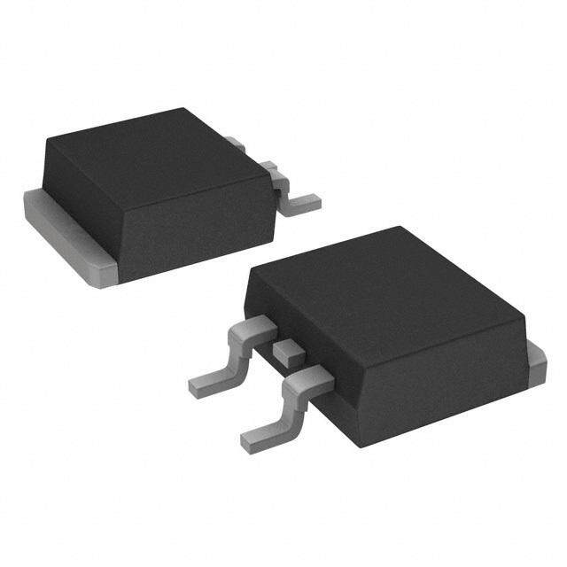
| 产品图片 |
|
| 产品型号 | SSM3K7002BSU,LF |
| rohs | 无铅 / 符合限制有害物质指令(RoHS)规范要求 |
| 产品系列 | - |
| 不同Id时的Vgs(th)(最大值) | 3.1V @ 250µA |
| 不同Vds时的输入电容(Ciss) | 17pF @ 25V |
| 不同Vgs时的栅极电荷(Qg) | - |
| 不同 Id、Vgs时的 RdsOn(最大值) | 2.1 欧姆 @ 500mA,10V |
| 产品培训模块 | http://www.digikey.cn/PTM/IndividualPTM.page?site=cn&lang=zhs&ptm=24813http://www.digikey.cn/PTM/IndividualPTM.page?site=cn&lang=zhs&ptm=30223 |
| 产品目录绘图 |
|
| 产品目录页面 | |
| 供应商器件封装 | USM |
| 其它名称 | SSM3K7002BFU(T5LFDKR |
| 功率-最大值 | 150mW |
| 包装 | Digi-Reel® |
| 安装类型 | 表面贴装 |
| 封装/外壳 | SC-70,SOT-323 |
| 标准包装 | 1 |
| 漏源极电压(Vdss) | 60V |
| 电流-连续漏极(Id)(25°C时) | 200mA (Ta) |


PDF Datasheet 数据手册内容提取
SSM3K7002BSU TOSHIBA Field-Effect Transistor Silicon N Channel MOS Type (U-MOSⅣ) SSM3K7002BSU High-Speed Switching Applications Analog Switch Applications Unit: mm • Small package • Low ON-resistance : RDS(ON) = 3.3 W (max) (@VGS = 4.5 V) : RDS(ON) = 2.6 W (max) (@VGS = 5 V) : RDS(ON) = 2.1 W (max) (@VGS = 10 V) Absolute Maximum Ratings (Ta = 25°C) Characteristics Symbol Rating Unit Drain-source voltage VDSS 60 V Gate-source voltage VGSS – 20 V DC ID 200 Drain current mA Pulse IDP 800 Power dissipation (Ta = 25°C) PD (Note 1) 150 mW 1. Gate Channel temperature Tch 150 °C 2. Source Storage temperature range Tstg - 55 to 150 °C 3. Drain Note: Using continuously under heavy loads (e.g. the application of high JEDEC SOT-323 temperature/current/voltage and the significant change in JEITA - temperature, etc.) may cause this product to decrease in the reliability significantly even if the operating conditions (i.e. TOSHIBA 2-2Z1A operating temperature/current/voltage, etc.) are within the Weight: 5.5 mg (typ.) absolute maximum ratings. Please design the appropriate reliability upon reviewing the Toshiba Semiconductor Reliability Handbook (“Handling Precautions”/“Derating Concept and Methods”) and individual reliability data (i.e. reliability test report and estimated failure rate, etc). Note 1: Mounted on FR4 board (25.4 mm · 25.4 mm · 1.6 mm, Cu Pad: 0.6mm2 · 3) 0.6 mm 1.0 mm Marking Equivalent Circuit (top view) 3 3 NM 1 2 1 2 1 2011-12-09
SSM3K7002BSU Electrical Characteristics (Ta = 25°C) Characteristics Symbol Test Condition Min Typ Max Unit Gate leakage current IGSS VGS = – 20 V, VDS = 0 V (cid:190) (cid:190) – 10 m A Drain-source breakdown voltage V (BR) DSS ID = 0.1 mA, VGS = 0 V 60 (cid:190) (cid:190) V V (BR) DSX ID = 0.1 mA, VGS = -10 V 45 (cid:190) (cid:190) Drain cutoff current IDSS VDS = 60 V, VGS = 0 V (cid:190) (cid:190) 1 m A Gate threshold voltage Vth VDS = 10 V, ID = 0.25 mA 1.0 (cid:190) 2.5 V Forward transfer admittance Yfs VDS = 10 V, ID = 200 mA (Note 2) 225 (cid:190) (cid:190) mS ID = 500 mA, VGS = 10 V (Note 2) (cid:190) 1.62 2.1 Drain-source ON-resistance RDS (ON) ID = 100 mA, VGS = 5 V (Note 2) (cid:190) 1.77 2.6 W ID = 100 mA, VGS = 4.5 V (Note 2) (cid:190) 1.81 3.3 Input capacitance Ciss (cid:190) 17.0 (cid:190) Reverse transfer capacitance Crss VDS = 25 V, VGS = 0 V, f = 1 MHz (cid:190) 1.9 (cid:190) pF Output capacitance Coss (cid:190) 3.6 (cid:190) Switching time TTuurrnn--oonff ddeellaayy ttiimmee ttdd((oonff)) VVDGDS == 30 0t oV 1, 0ID V = 200 mA , (cid:190)(cid:190) 21.85 55.50 ns Drain-source forward voltage VDSF ID = -200 mA, VGS = 0 V (Note 2) (cid:190) -0.84 -1.2 V Note2: Pulse test Switching Time Test Circuit (a) Test circuit (b) VIN 10 V 90 % 10 V IN OUT 10 % 0 V 0 W50 RL (c) VOUT VDD 90 % 10 m s VDD VDDutDy£ =£££ 310% V VDS (ON) 10 % VIN: tr, tf < 2 ns tr tf (Zout = 50 W ) Common Source td(on) Ta = 25 °C td(off) Precaution Let Vth be the voltage applied between gate and source that causes the drain current (ID) to be low (0.25 mA for the SSM3K7002BSU). Then, for normal switching operation, VGS(on) must be higher than Vth, and VGS(off) must be lower than Vth. This relationship can be expressed as: VGS(off) < Vth < VGS(on). Take this into consideration when using the device Handling Precaution When handling individual devices that are not yet mounted on a circuit board, make sure that the environment is protected against electrostatic discharge. Operators should wear antistatic clothing, and containers and other objects that come into direct contact with devices should be made of antistatic materials. 2 2011-12-09
SSM3K7002BSU ID – VDS ID – VGS 1000 1000 Common Source Common Source Ta = 25 °C 7.0 V 5.0 V VDS = 10 V (mA) 800 10 V 44..50 VV mA) 100 ( I D 600 D Ta = 100 °C I current 400 33..35 VV urrent 10 25 °C Drain 200 VGS = 2.5 Drain c 1 2.8V -25 °C 0 0.1 0 0.4 0.8 1.2 1.6 2.0 0 1.0 2.0 3.0 4.0 5.0 Drain–source voltage VDS (V) Gate–source voltage VGS (V) RDS (ON) – ID RDS (ON) – VGS 5 5 Common Source ID = 100 mA Ta = 25°C Common Source Drain–source ON-resistance ΩR () DS (ON) 2143 VGS = 10 V 4.05V.0 V 4.5 V Drain–source ON-resistance ΩR () DS (ON) 2431 Ta = 2T5a°C =- 2 12505 °0 C°C ° C 0 0 10 30 100 300 1000 0 10 20 Drain current ID (mA) Gate–source voltage VGS (V) RDS (ON) – Ta Vth – Ta 5 3.0 Common Source Common Source V) VDS = 10 V ce 4 (h ID = 0.25 mA an Vt ON-resistΩ () N) 3 100 mA / 4.5 V voltage 2.0 e O d ain–sourcRDS ( 21 ID = 500 mA / VGS = 10 V e threshol 1.0 Dr at G 100 mA / 5.0V 0 0 - 50 0 50 100 150 - 50 0 50 100 150 Ambient temperature Ta (°C) Ambient temperature Ta (°C) 3 2011-12-09
SSM3K7002BSU |Yfs| – ID IDR – VDS 1 1000 S) Common Source Common Source Y (fs 0.3 VTaD =S 2=5 1°C0 V (mA) 800 VT aG =S 2=5 0°C DV ance 0.1 nt I DR 600 G S IDR sfer admitt 00..0013 erse curre 400 n v a e ward tr 0.003 Drain r 200 or F 0.001 0 1 10 100 1000 0 -0.2 -0.4 -0.6 -0.8 -1.0 -1.2 Drain current ID (mA) Drain–source voltage VDS (V) C – VDS t – ID 100 1000 tf Common Source VDD = 30 V pF) 50 VTaG =S 2=5 0 °C to 10 V C ( 30 Ciss (ns) 100 td(off) e c t n cita 10 me Capa 5 ng ti 10 hi 3 CTf a=o m=1 m2M5oH°Cnz Source CCrossss Switc td(on) VGS = 0 V tr 1 1 0.1 1 10 100 1 10 100 1000 Drain–source voltage VDS (V) Drain current ID (mA) PD – Ta 250 W) M(2o5u.4n tmedm o ·n 2F5R.44 mboma r·d .1 .6 mm, Cu Pad: 0.6 mm2 · 3) m ( 200 D P n o 150 ati p si s di 100 er w o p n 50 ai Dr 0 0 40 80 120 160 Ambient temperature Ta (°C) 4 2011-12-09
SSM3K7002BSU RESTRICTIONS ON PRODUCT USE • Toshiba Corporation, and its subsidiaries and affiliates (collectively “TOSHIBA”), reserve the right to make changes to the information in this document, and related hardware, software and systems (collectively “Product”) without notice. • This document and any information herein may not be reproduced without prior written permission from TOSHIBA. Even with TOSHIBA’s written permission, reproduction is permissible only if reproduction is without alteration/omission. • Though TOSHIBA works continually to improve Product’s quality and reliability, Product can malfunction or fail. Customers are responsible for complying with safety standards and for providing adequate designs and safeguards for their hardware, software and systems which minimize risk and avoid situations in which a malfunction or failure of Product could cause loss of human life, bodily injury or damage to property, including data loss or corruption. Before customers use the Product, create designs including the Product, or incorporate the Product into their own applications, customers must also refer to and comply with (a) the latest versions of all relevant TOSHIBA information, including without limitation, this document, the specifications, the data sheets and application notes for Product and the precautions and conditions set forth in the “TOSHIBA Semiconductor Reliability Handbook” and (b) the instructions for the application with which the Product will be used with or for. Customers are solely responsible for all aspects of their own product design or applications, including but not limited to (a) determining the appropriateness of the use of this Product in such design or applications; (b) evaluating and determining the applicability of any information contained in this document, or in charts, diagrams, programs, algorithms, sample application circuits, or any other referenced documents; and (c) validating all operating parameters for such designs and applications. TOSHIBA ASSUMES NO LIABILITY FOR CUSTOMERS’ PRODUCT DESIGN OR APPLICATIONS. • Product is intended for use in general electronics applications (e.g., computers, personal equipment, office equipment, measuring equipment, industrial robots and home electronics appliances) or for specific applications as expressly stated in this document. Product is neither intended nor warranted for use in equipment or systems that require extraordinarily high levels of quality and/or reliability and/or a malfunction or failure of which may cause loss of human life, bodily injury, serious property damage or serious public impact (“Unintended Use”). Unintended Use includes, without limitation, equipment used in nuclear facilities, equipment used in the aerospace industry, medical equipment, equipment used for automobiles, trains, ships and other transportation, traffic signaling equipment, equipment used to control combustions or explosions, safety devices, elevators and escalators, devices related to electric power, and equipment used in finance-related fields. Do not use Product for Unintended Use unless specifically permitted in this document. • Do not disassemble, analyze, reverse-engineer, alter, modify, translate or copy Product, whether in whole or in part. • Product shall not be used for or incorporated into any products or systems whose manufacture, use, or sale is prohibited under any applicable laws or regulations. • The information contained herein is presented only as guidance for Product use. No responsibility is assumed by TOSHIBA for any infringement of patents or any other intellectual property rights of third parties that may result from the use of Product. No license to any intellectual property right is granted by this document, whether express or implied, by estoppel or otherwise. • ABSENT A WRITTEN SIGNED AGREEMENT, EXCEPT AS PROVIDED IN THE RELEVANT TERMS AND CONDITIONS OF SALE FOR PRODUCT, AND TO THE MAXIMUM EXTENT ALLOWABLE BY LAW, TOSHIBA (1) ASSUMES NO LIABILITY WHATSOEVER, INCLUDING WITHOUT LIMITATION, INDIRECT, CONSEQUENTIAL, SPECIAL, OR INCIDENTAL DAMAGES OR LOSS, INCLUDING WITHOUT LIMITATION, LOSS OF PROFITS, LOSS OF OPPORTUNITIES, BUSINESS INTERRUPTION AND LOSS OF DATA, AND (2) DISCLAIMS ANY AND ALL EXPRESS OR IMPLIED WARRANTIES AND CONDITIONS RELATED TO SALE, USE OF PRODUCT, OR INFORMATION, INCLUDING WARRANTIES OR CONDITIONS OF MERCHANTABILITY, FITNESS FOR A PARTICULAR PURPOSE, ACCURACY OF INFORMATION, OR NONINFRINGEMENT. • Do not use or otherwise make available Product or related software or technology for any military purposes, including without limitation, for the design, development, use, stockpiling or manufacturing of nuclear, chemical, or biological weapons or missile technology products (mass destruction weapons). Product and related software and technology may be controlled under the Japanese Foreign Exchange and Foreign Trade Law and the U.S. Export Administration Regulations. Export and re-export of Product or related software or technology are strictly prohibited except in compliance with all applicable export laws and regulations. • Please contact your TOSHIBA sales representative for details as to environmental matters such as the RoHS compatibility of Product. Please use Product in compliance with all applicable laws and regulations that regulate the inclusion or use of controlled substances, including without limitation, the EU RoHS Directive. TOSHIBA assumes no liability for damages or losses occurring as a result of noncompliance with applicable laws and regulations. 5 2011-12-09