ICGOO在线商城 > 集成电路(IC) > PMIC - 稳压器 - 线性 > SPX5205M5-L

 Datasheet下载
- 型号: SPX5205M5-L
- 制造商: Exar
- 库位|库存: xxxx|xxxx
- 要求:
| 数量阶梯 | 香港交货 | 国内含税 |
| +xxxx | $xxxx | ¥xxxx |
查看当月历史价格
查看今年历史价格
SPX5205M5-L产品简介:
ICGOO电子元器件商城为您提供SPX5205M5-L由Exar设计生产,在icgoo商城现货销售,并且可以通过原厂、代理商等渠道进行代购。 SPX5205M5-L价格参考。ExarSPX5205M5-L封装/规格:PMIC - 稳压器 - 线性, Linear Voltage Regulator IC Positive Adjustable 1 Output Adjustable 150mA SOT-23-5。您可以下载SPX5205M5-L参考资料、Datasheet数据手册功能说明书,资料中有SPX5205M5-L 详细功能的应用电路图电压和使用方法及教程。
| 参数 | 数值 |
| 产品目录 | 集成电路 (IC)半导体 |
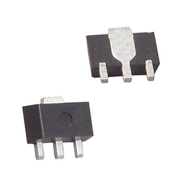
| 描述 | IC REG LDO ADJ 0.15A SOT23-5低压差稳压器 2.5V-16V 150mA |
| 产品分类 | |
| 品牌 | Exar |
| 产品手册 | |
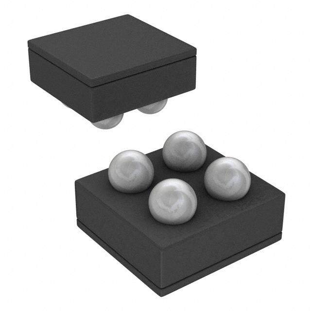
| 产品图片 |
|
| rohs | 符合RoHS无铅 / 符合限制有害物质指令(RoHS)规范要求 |
| 产品系列 | 电源管理 IC,低压差稳压器,Exar SPX5205M5-L- |
| 数据手册 | http://www.exar.com/Common/Content/Document.ashx?id=618 |
| 产品型号 | SPX5205M5-L |
| PCN设计/规格 | |
| 产品种类 | 低压差稳压器 |
| 供应商器件封装 | SOT-23-5 |
| 其它名称 | 1016-1250 |
| 包装 | 散装 |
| 商标 | Exar |
| 安装类型 | 表面贴装 |
| 安装风格 | SMD/SMT |
| 封装 | Bulk |
| 封装/外壳 | SC-74A,SOT-753 |
| 封装/箱体 | SOT-23-5 |
| 工作温度 | -40°C ~ 85°C |
| 最大工作温度 | + 125 C |
| 最大输入电压 | 16 V |
| 最小工作温度 | - 40 C |
| 最小输入电压 | + 2.5 V |
| 标准包装 | 50 |
| 电压-跌落(典型值) | 0.21V @ 150mA |
| 电压-输入 | 2.5 V ~ 16 V |
| 电压-输出 | 可调 |
| 电压调节准确度 | 1 % |
| 电流-输出 | 150mA |
| 电流-限制(最小值) | - |
| 稳压器拓扑 | 正,可调式 |
| 稳压器数 | 1 |
| 线路调整率 | 0.1 % / V |
| 负载调节 | 0.2 % |
| 输入偏压电流—最大 | 0.00005 mA |
| 输出电流 | 150 mA |
| 输出端数量 | 1 Output |
| 输出类型 | Adjustable, Fixed |


PDF Datasheet 数据手册内容提取
SPX5205 150mA, Low-Noise LDO Voltage Regulator Description FEATURES The SPX5205 is a positive voltage regulator with very low dropout ■■ Low Noise Output LDO: 40μVRMS voltage, output noise and ground current (750μA at 100mA). V has Possible OUT a tolerance of less than 1% and is temperature compensated. Fixed ■■ 1% Initial Accuracy output voltages 1.8V, 3.0V, 3.3V, and 5.0V and an adjustable version ■■ Very Low Quiecent Current: 70μA are available in a small 5-pin SOT-23 package. Other key features ■■ Low Dropout Voltage (210mV at 150mA) include zero off-mode current, reverse battery protection, thermal ■■ Current and Thermal Limiting shutdown and current limit. The SPX5205 is an excellent choice for ■■ Reverse-Battery Protection use in batterypowered applications, and where power conservation is ■■ Wide Range of Fixed Output Voltages: 1.8V, 3.0V, 3.3V and 5.0V desired such as: cellular/ cordless telephones, radio control systems and portable computers. ■■ Zero Off-Mode Current ■■ Small 5-Pin SOT-23 ■■ Pin Compatible to MIC5205/MAX8877 Top View Top View (fixed options only) and LP2985 VOUT BYP VOUT ADJ APPLICATIONS ■■ PDA ■■ Battery Powered Systems 5 4 5 4 ■■ Cellular Phone SPX5205 SPX5205 ■■ Cordless Telephones ■■ Radio Control Systems 1 2 3 1 2 3 ■■ Laptop, Palmtop and Notebook Computers ■■ Portable Consumer Equipment ■■ Portable Instrumentation VIN GND EN VIN GND EN ■■ Bar Code Scanners Fixed Output Voltage Adjustable Output Voltage ■■ SMPS Post-Regulator Ordering Information - Back Page Typical Applications Circuit V 1 5 V IN OUT + 1.0µF 2 SPX5205 + GND 3 4 EN BYP 5-pin Fixed ENABLE may be tied directly to V IN TOP View REV L 1/8
SPX5205 Absolute Maximum Ratings Recommended Operating Conditions These are stress ratings only and functional operation of the Input Supply Voltage ....................................+2.5V to +16V device at these ratings or any other above those indicated Operating Junction Temperature Range ....-40˚C to +125˚C in the operation sections of the specifications below is not implied. Exposure to absolute maximum rating conditions Enable Input Voltage .............................................0V to VIN for extended periods of time may affect reliability. SOT-23-5 (ѳ ) ..................................................See Note 1 JA Thermal Shutdown ....................................Internally limited Lead Temperature (Soldering, 5 seconds) .................260˚C Input Supply Voltage ......................................-20V to +20V Enable Input Voltage ......................................-20V to +20V Electrical Characteristics TJ = 25°C, VIN = VOUT + 1V, IL = 100μA, CL = 1μF, and VENABLE ≥ 2.4V. The “•” denotes the specifications which apply over full junction temperature range -40°C to +125°C, unless otherwise specified. PARAMETER MIN. TYP. MAX. UNITS • CONDITIONS -1 +1 Output voltage tolerance (VOUT) %VNOM -2 +2 • Output voltage temperature 57 ppm/°C • coefficient 0.03 0.1 VIN = VOUT + 1 to 16V and VEN ≤ 6V Line regulation 0.2 %/V • VIN = VEN = VOUT + 1 ≤ 8V 0.2 VIN = VEN = VOUT + 1 to 16V TA = 25°C to 85°C 0.1 0.2 VIN = VOUT + 1 ≥ 2.5V Load regulation 0.5 % • IL= 1mA to 150mA 1.0 • IL= 100µA to 1mA 30 50 mV IL= 100µA 70 • 140 190 mV IL= 50mA Dropout voltage(2) 230 • (VIN - VO) 180 250 mV IL= 100mA 300 • 210 275 mV IL= 150mA 350 • 0.05 1 VENABLE ≤ 0.4V Quiescent current (IGND) µA 5 • VENABLE ≤ 0.25V 70 125 µA IL= 100µA 150 • 350 600 µA IL= 50mA 800 • Ground pin current (IGND) 750 1000 µA IL= 100mA 1500 • 1300 1900 µA IL= 150mA 2500 • REV L 2/8
SPX5205 Electrical Characteristics (Continued) TJ = 25°C, VIN = VOUT + 1V, IL = 100μA, CL = 1μF, and VENABLE ≥ 2.4V. The “•” denotes the specifications which apply over full junction temperature range -40°C to +125°C, unless otherwise specified. PARAMETER MIN. TYP. MAX. UNITS • CONDITIONS Ripple rejection 70 dB Current limit (ILIMIT) 360 500 mA VOUT = 0V 300 IL = 10mA, CL = 1µF, CIN = 1µF (10Hz - 100kHz) Output noise (eNO) µVRMS 40 IL = 10mA, CL = 10µF, CBYP = 1µF, CIN = 1µF (10Hz - 100kHz) Input voltage level logic low (VIL) 0.4 V OFF Input voltage level logic high (VIL) 2.0 V ON 0.01 2 VIL ≤ 0.4V Enable input current µA 3 20 VIH ≥ 2.0V NOTE: 1. The maximum allowable power dissipation is a function of maximum operating junction temperature, TJ(max), the junction to ambient thermal resistance, and the ambient ѳJA, and the ambient temperature TA. The maximum allowable power dissipation at any ambient temperature is given: PD(max) = (TJ(max) - TA) / ѳJA, exceeding the maximum allowable power limit will result in excessive die temperature; thus, the regulator will go into thermal shutdown. The ѳJA of the SPX5205 is 220°C/W mounted on a PC board. 2. Not applicable to output voltages of less than 2V. REV L 3/8
SPX5205 Typical Performance Characteristics 110 1.40 100 1.20 3.3V Device CVLIN == 13..02μVF 90 1.00 80 (mA) 0.80 (A)µD 70 D N N 0.60 G G I 60 I 0.40 50 VO = 3.3V CL = 1.0µF IL = 100μA 0.20 40 30 0.00 4 6 8 10 12 14 16 0 50 100 150 IL (mA) VIN (V) Figure 1. Ground Current vs. Load Current Figure 2. Ground Current vs. Input Voltage 2.00 3.340 3.335 3.3V Device VIN= 4.3V 3.330 1.50 CL = 1.0µF 3.325 ) mA) (VT 3.320 (D 1.00 OU 3.315 N V G 3.310 I 3.305 3.3V Device 0.50 3.300 CL= 1.0μF IL = 100μA 3.295 3.290 0.00 4 6 8 10 12 14 16 0 50 100 150 IL (mA) VIN (V) Figure 3. Ground Current vs. Load Current in Dropout Figure 4. Output Voltage vs. Input Voltage 3.310 200 VO=3.3V 3.3V Device VIN= 3.2V VIN= 4.3V CL = 1.0µF 3.308 CL = 1.0µF ) 150 V (m V) 3.306 ut (T o U p 100 O ro V 3.304 D 50 3.302 0 3.300 0 50 100 150 0 50 100 150 IL (mA) IL (mA) Figure 5. Dropout Voltage vs. Load Current Figure 6. Output Voltage vs. Load Current REV L 4/8
SPX5205 Typical Performance Characteristics (Continued) 90.0 950 VOUT= 3.3V VIN= 4.3V 80.0 CL= 1.0μF 850 IL = 100μA A) ) 750 m A (GND 70.0 (μGND 650 I I 60.0 VOUT = 3.3V 550 VIN = 4.3V CL= 1.0μF IL = 100mA 50.0 450 -40 -20 0 20 40 60 80 100 120 -40 -20 0 20 40 60 80 100 120 Temperature ( °C) Temperature ( °C) Figure 7. Ground Current vs. Temperature Figure 8. Ground Current vs. Temperature at I = 100μA at I = 100mA LOAD LOAD 3.400 2.30 3.380 VOUT= 3.3V 2.20 VOUT= 3.3V VIN= 4.3V 2.10 VCLIN== 1 4.0.3μVF 33..336400 CL= 1.0μF 2.00 IL = 150mA A) V) 3.320 (mND 11..9800 V(OUT 32..320800 G I 1.70 2.260 1.60 2.240 1.50 2.220 1.40 2.200 -40 -20 0 20 40 60 80 100 120 -40 -20 0 20 40 60 80 100 120 Temperature ( °C) Temperature ( °C) Figure 9. Ground Current in Dropout vs. Temperature Figure 10. Output Voltage vs. Temperature 1.60 350 1.50 CVLO=U T1 .=03μ.F3V 300 CCCioinnu ==t =11 uu1FFuTTF,,T IL = 100μA Cout = 2.2uFT V) 1.40 Cin = 1uFT old( 1.30 250 Cout = 10uFT h s 200 n Thre 11..2100 uV RMS 150 O EN, 1.00 100 V 0.90 50 0.80 4 6 8 10 12 14 16 0 1 10 100 1000 10000 100000 1000000 VIN (V) Bypass Cap (pF) Figure 11. ENABLE Voltage, Figure 12. Output Noise vs. Bypass Capacitor Value ON Threshold vs. Input Voltage REV L 5/8
SPX5205 Application Information The SPX5205 requires an output capacitor for device Typical Applications Circuits stability. Its value depends upon the application circuit. In A 10nF capacitor on the BYP pin will significantly reduce general, linear regulator stability decreases with higher output noise but it may be left unconnected if the output output currents. In applications where the SPX5205 is noise is not a major concern. The SPX5205 start-up speed putting out less current, a lower output capacitance may is inversely proportional to the size of the BYP capacitor. be sufficient. For example, a regulator sourcing only 10mA, Applications requiring a slow ramp-up of the output voltage requires approximately half the capacitance as the same should use a larger CBYP. However, if a rapid turn-on is regulator sourcing 150mA. necessary, the BYP capacitor can be omitted. Bench testing is the best method for determining the proper The SPX5205’s internal reference is available through the type and value of the capacitor since the high frequency BYP pin. characteristics of electrolytic capacitors vary widely, The Typical Application Circuit shown on page 1 represents depending on type and manufacturer. A high quality 2.2μF a SPX5205 standard application circuit. The EN (enable) aluminum electrolytic capacitor works in most application pin is pulled high (>2.0V) to enable the regulator. To disable circuits, but the same stability often can be obtained with a the regulator, EN < 0.4V. 1μF tantalum electrolytic. The SPX5205 in Figure 13 illustrates a typical adjustable With the SPX5205 adjustable version, the minimum value of output voltage configuration. Two resistors (R1 and R2) set output capacitance is a function of the output voltage. The the output voltage. The output voltage is calculated using value decreases with higher output voltages, since closed the formula: loop gain is increased. V = 1.235V x (1 + R1/R2) OUT R2 must be >10 kΩ, and for best results, R2 should be between 22 kΩ and 47kΩ. V 1 5 V IN OUT + 2 R1 SPX5205 + GND 3 4 ADJ EN 5-pin Adjustable Hi-ON R2 Lo-OFF TOP View Figure 13. Typical Adjustable Output Voltage REV L 6/8
SPX5205 Mechanical Dimensions SOT-23-5 F O R R E F E R E N C E O N L Y REV L 7/8
SPX5205 Ordering Information(1) Operating Part Number Lead-Free Package Packaging Method Accuracy Output Voltage Temperature Range SPX5205M5-L/TR Adjustable SPX5205M5-L-1-8/TR 1.8V SPX5205M5-L-3-0/TR -40°C ≤ TJ ≤ 125°C Yes(2) 5-pin SOT-23 Tape and Reel 1% 3.0V SPX5205M5-L-3-3/TR 3.3V SPX5205M5-L-5-0/TR 5.0V NOTE: 1. Refer to www.exar.com/SPX5205 for most up-to-date Ordering Information. 2. Visit www.exar.com for additional information on Environmental Rating. Revision History Revision Date Description K -- Sipex / Exar legacy datasheet Update to MaxLinear logo. Update format and Ordering Information. Added Figure numbers. L 8/31/18 Corrected CL unit in Figure 11. Updated Typical Application Circuit on page 1 and Figure 13 to differentiate between fixed and adjustable versions. Updated last paragraph of Typical Applications Circuits section. Updated temperature at top of Electrical Characteristics. Corporate Headquarters: High Performance Analog: 5966 La Place Court 1060 Rincon Circle Suite 100 San Jose, CA 95131 Carlsbad, CA 92008 Tel.: +1 (669) 265-6100 Tel.:+1 (760) 692-0711 Fax: +1 (669) 265-6101 Fax: +1 (760) 444-8598 www.exar.com www.maxlinear.com The content of this document is furnished for informational use only, is subject to change without notice, and should not be construed as a commitment by MaxLinear, Inc.. MaxLinear, Inc. assumes no responsibility or liability for any errors or inaccuracies that may appear in the informational content contained in this guide. Complying with all applicable copyright laws is the responsibility of the user. Without limiting the rights under copyright, no part of this document may be reproduced into, stored in, or introduced into a retrieval system, or transmitted in any form or by any means (electronic, mechanical, photocopying, recording, or otherwise), or for any purpose, without the express written permission of MaxLinear, Inc. Maxlinear, Inc. does not recommend the use of any of its products in life support applications where the failure or malfunction of the product can reasonably be expected to cause failure of the life support system or to significantly affect its safety or effectiveness. Products are not authorized for use in such applications unless MaxLinear, Inc. receives, in writing, assurances to its satisfaction that: (a) the risk of injury or damage has been minimized; (b) the user assumes all such risks; (c) potential liability of MaxLinear, Inc. is adequately protected under the circumstances. MaxLinear, Inc. may have patents, patent applications, trademarks, copyrights, or other intellectual property rights covering subject matter in this document. Except as expressly provided in any written license agreement from MaxLinear, Inc., the furnishing of this document does not give you any license to these patents, trademarks, copyrights, or other intellectual property. Company and product names may be registered trademarks or trademarks of the respective owners with which they are associated. © 2001 - 2018 MaxLinear, Inc. All rights reserved SPX5205_DS_083118 REV L 8/8
Mouser Electronics Authorized Distributor Click to View Pricing, Inventory, Delivery & Lifecycle Information: E xar: SPX5205M5-L SPX5205M5-L-3-3 SPX5205M5-L/TR SPX5205M5-L-5-0/TR SPX5205M5-L-3-3/TR SPX5205M5-L- 1-2/TR SPX5205M5-L-3-0/TR SPX5205M5-L-1-8/TR SPX5205M5-L-2-5/TR SPX5205M5-L-1-2 SPX5205M5-L-1-8 SPX5205M5-L-2-5 SPX5205M5-L-3-0 SPX5205M5-L-5-0