ICGOO在线商城 > 集成电路(IC) > PMIC - 稳压器 - 线性 > SPX29502T5-L
- 型号: SPX29502T5-L
- 制造商: Exar
- 库位|库存: xxxx|xxxx
- 要求:
| 数量阶梯 | 香港交货 | 国内含税 |
| +xxxx | $xxxx | ¥xxxx |
查看当月历史价格
查看今年历史价格
SPX29502T5-L产品简介:
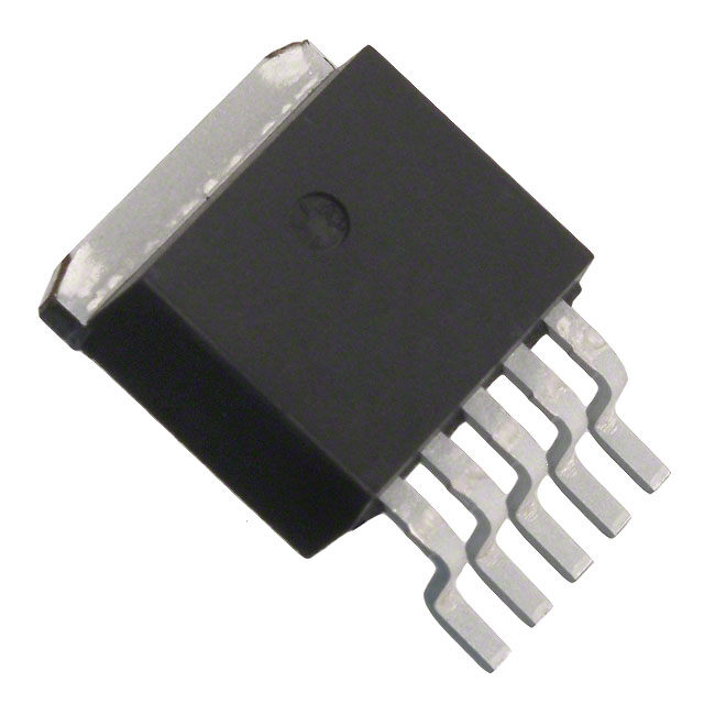
ICGOO电子元器件商城为您提供SPX29502T5-L由Exar设计生产,在icgoo商城现货销售,并且可以通过原厂、代理商等渠道进行代购。 SPX29502T5-L价格参考。ExarSPX29502T5-L封装/规格:PMIC - 稳压器 - 线性, Linear Voltage Regulator IC Positive Adjustable 1 Output 1.24 V ~ 16 V 5A TO-263-5。您可以下载SPX29502T5-L参考资料、Datasheet数据手册功能说明书,资料中有SPX29502T5-L 详细功能的应用电路图电压和使用方法及教程。
| 参数 | 数值 |
| 产品目录 | 集成电路 (IC)半导体 |
| 描述 | IC REG LDO ADJ 5A TO263-5低压差稳压器 2.8V-16V 5000mA |
| 产品分类 | |
| 品牌 | Exar Corporation |
| 产品手册 | |
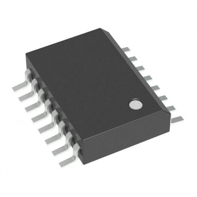
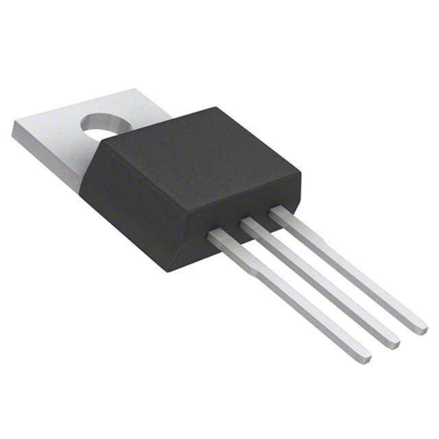
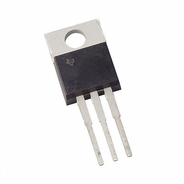
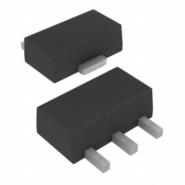
| 产品图片 |
|
| rohs | 符合RoHS无铅 / 符合限制有害物质指令(RoHS)规范要求 |
| 产品系列 | 电源管理 IC,低压差稳压器,Exar SPX29502T5-L- |
| 数据手册 | http://www.exar.com/Common/Content/Document.ashx?id=660 |
| 产品型号 | SPX29502T5-L |
| 产品种类 | 低压差稳压器 |
| 供应商器件封装 | TO-263-5 |
| 其它名称 | 1016-1246-5 |
| 包装 | 管件 |
| 参考电压 | 1.24 V |
| 商标 | Exar |
| 回动电压—最大值 | 800 mV |
| 安装类型 | 表面贴装 |
| 安装风格 | SMD/SMT |
| 封装 | Tube |
| 封装/外壳 | TO-263-6,D²Pak(5 引线+接片),TO-263BA |
| 封装/箱体 | TO-263-5 |
| 工作温度 | -40°C ~ 125°C |
| 工厂包装数量 | 50 |
| 最大工作温度 | + 125 C |
| 最大输入电压 | 16 V |
| 最小工作温度 | - 40 C |
| 最小输入电压 | 2.8 V |
| 标准包装 | 50 |
| 电压-跌落(典型值) | 0.42V @ 5A |
| 电压-输入 | 2.8 V ~ 16 V |
| 电压-输出 | 1.24 V ~ 16 V |
| 电压调节准确度 | 1 % |
| 电流-输出 | 5A |
| 电流-限制(最小值) | - |
| 稳压器拓扑 | 正,可调式 |
| 稳压器数 | 1 |
| 线路调整率 | 0.5 % |
| 负载调节 | 1 % |
| 输出电压 | 14.45 V to 1.25 V |
| 输出电流 | 5 A |
| 输出端数量 | 1 Output |
| 输出类型 | Adjustable |






- 商务部:美国ITC正式对集成电路等产品启动337调查
- 曝三星4nm工艺存在良率问题 高通将骁龙8 Gen1或转产台积电
- 太阳诱电将投资9.5亿元在常州建新厂生产MLCC 预计2023年完工
- 英特尔发布欧洲新工厂建设计划 深化IDM 2.0 战略
- 台积电先进制程称霸业界 有大客户加持明年业绩稳了
- 达到5530亿美元!SIA预计今年全球半导体销售额将创下新高
- 英特尔拟将自动驾驶子公司Mobileye上市 估值或超500亿美元
- 三星加码芯片和SET,合并消费电子和移动部门,撤换高东真等 CEO
- 三星电子宣布重大人事变动 还合并消费电子和移动部门
- 海关总署:前11个月进口集成电路产品价值2.52万亿元 增长14.8%



PDF Datasheet 数据手册内容提取
® P SPX29501/02 55AA LLooww DDrrooppoouutt VVoollttaaggee RReegguullaattoorr November 2008 5 Rev. B A FEATURES ■ Adjustable Output Down to 1.25V ■ 1% Output Accuracy ■ Output Current of 5A ■ Low Dropout Voltage: 420mV @ 5A ■ Tight Line Regulation: 0.06% SPX29502 ■ Load Regulation: 0.2% SP29500 ■ Fast Transient Response 5 Pin TO-263 3 Pin TO-220 ■ Reverse-Battery Protection 1 2 3 ■ Current Limit and Thermal Protection 1 2 3 APPLICATIONS ■ Powering VGA & Sound Card ■ Power PC™ Supplies N T D T T ■■ SHMigPh SE fPfiocisetn Rcey g“uGlaretoern” Computer E INPU GN OUTPU ADJUS Systems V GND V IN OUT ■ High Efficiency Linear Power Supplies ■ Constant Current Regulators Now Available in Lead Free Packaging ■ Adjustable Power Supplies ■ Battery Charger DESCRIPTION The SPX29501/02 are 5A highly accurate voltage regulators with a low dropout voltage of 420mV @ 5A. These regulators are specifically designed for low voltage applications that require a low dropout voltage and a fast transient response. They are fully fault protected against over-current, reverse battery, and positive and negative voltage transients. On-Chip trimming adjusts the reference voltage to 1% initial accuracy. Other features include Enable, and Error Flag. The SPX295001/02 are offered in 5-pin TO-220 & TO-263 packages. For a 1.5A version, refer to the SPX29150 data sheet. For a 3A version, refer to the SPX29300 datasheet. TYPICAL APPLICATION CIRCUITS VIN 1 SPX29500 3 VOUT VIN 1 SPX29502 4 VOUT 2 6.8µF+ 2 + 22µF 6.8µF+ 3 5ADJ R1+ 22µF GND R2 Figure 1. Fixed Output Linear Regulator Figure 2. Adjustable Output Linear Regulator Exar Corporation www.exar.com 48720 Kato Road, Fremont CA 94538, USA Tel. +1 510 668-7000 – Fax. +1 510 668-7001
ABSOLUTE MAXIMUM RATINGS OPERATING RATINGS Lead Temperature (soldering, 5 seconds) ................260°C Input Voltage...................................................................16V Storage Temperature Range........................-65°C to +150°C Operating Junction Temperature Range......-40°C to +125°C Input Voltage (Note 1)....................................................20V ELECTRICAL CHARACTERISTICS Specifications are at VIN = VOUT + 1V and IOUT = 10mA, CIN = 6.8µF, COUT = 22µF, TA = 25°C, unless otherwise specified. The ♦ denotes the specifications which apply over the full operating temperature range, unless otherwise specified. PARAMETER MIN TYP MAX UNITS CONDITIONS Fixed Voltage Options SPX29501 1.8V Version Output Voltage 1.782 1.800 1.818 V I = 10mA OUT 1.764 1.800 1.836 ♦ 10mA ≤ IOUT ≤ 5A, 2.8V ≤ VIN ≤ 16V 2.5V Version Output Voltage 2.475 2.500 2.525 V I = 10mA OUT 2.450 2.500 2.550 ♦ 10mA ≤ IOUT ≤ 5A, 3.5V ≤ VIN ≤ 16V 3.3V Version Output Voltage 3.267 3.300 3.333 V I = 10mA OUT 3.234 3.300 3.366 ♦ 10mA ≤ IOUT ≤ 5A, 4.3V ≤ VIN ≤ 16V 5.0V Version Output Voltage 4.950 5.000 5.050 V I = 10mA OUT 4.900 5.000 5.100 ♦ 10mA ≤ IOUT ≤ 5A, 6.0V ≤ VIN ≤ 16V All Voltage Options SPX29501/02 Line Regulation 0.06 0.5 % IOUT=10mA,(VOUT+1V) ≤ VIN ≤ 16V Load Regulation 0.2 1 % VIN=VOUT+2V, 10mA≤ IOUT ≤ IFL (Note 2) ∆V/∆T 20 100 ppm/°C ♦ VOUT Temp Coefficient (Note 5) Dropout Voltage, except 90 250 mV ♦ IOUT=250mA 1.8V 250 eg IOUT=2.5A 420 800 ♦ IOUT=5A Ground Current 20 50 mA ♦ IOUT=2.5A (Note 4) 70 I =5A OUT Ground Pin Current 3 mA V =0.5V less than specified V IN OUT, at Dropout I =10mA OUT Current Limit 7.5 10 A ♦ (Note 3) Output Noise Voltage 425 µVRMS CL=22µF (10Hz to 100kHz) IL=100mA 350 CL=33µF Reference Voltage 1.228 1.240 1.252 V Adjustable version only 1.215 1.265 ♦ Reference Voltage 1.203 1.277 V Adjustable version only (Note 7) Adjust Pin Bias Current 40 80 nA 120 ♦ Reference Voltage 20 ppm/°C (Note 6) Temp. Coeff. Adjust Pin Bias 0.1 nA/°C Current Temp. Coeff. Rev:B Nov 2008 SPX29500/01/02/03 5A Low Dropout Voltage Regulator © Copyright 2008 Exar Corporation 2
ELECTRICAL CHARACTERISTICS: Continued Specifications are at VIN = VOUT + 1V and IOUT = 10mA, CIN = 6.8µF, COUT = 22µF, TA = 25°C, unless otherwise specified. The ♦ denotes the specifications which apply over the full operating temperature range, unless otherwise specified. PARAMETER MIN TYP MAX UNITS CONDITIONS Flag Output (Error Comparator) SPX29501 Output Leakage 0.01 1 µA VOH=16V Current 2 ♦ Output Low Voltage 220 300 mV Device set for 5V,VIN=4.5V, IOL=250µA 400 ♦ Upper Threshold 40 60 mV Device set for 5V, (Note 8) Voltage 25 ♦ Lower Threshold 75 95 mV Device set for 5V, (Note 8) Voltage 140 ♦ Hysteresis 15 mV Device set for 5V, (Note 8) Enable Input SPX29501/02 Input Logic Voltage Low (OFF) 0.8 V (Note 10) High (ON) 2.4 ENABLE Input Current 100 600 µA VEN=16V 750 ♦ 0.6 2 µA VEN=0.8V 4 ♦ Regulator Output 10 µA (Note 9) Current in Shutdown 500 ♦ Thermal Resistance 2 °C/W TO-220 Junction to Case, at Tab 60 TO-220 Junction to Ambient 2 TO-263 Junction to Case, at Tab 60 TO-263 Junction to Ambient NOTES: Note 1: Maximum positive supply voltage of 20V must be of limited duration (<100ms) and duty cycle of less than 1%. The maximum continuous supply voltage is 16V. Note 2: Full load current (IFL) is defined as 5A. Note 3: VIN = VOUT (NOMINAL) +1V. For example, use VIN = 4.3V for a 3.3V regulator. Employ pulse-testing procedures to minimize temperature rise. Note 4 Ground pin current is the regulator quiescent current. The total current drawn from the source is the sum of the load current plus the ground pin current. Note 5: Output voltage temperature coefficient is defined as the worst case voltage change divided by the total temperature range. Note 6: Thermal regulation is defined as the change in output voltage at time T after a change in power dissipation is applied, excluding load / line regulation effects. Specifications for a 200mA load pulse as VIN = 20V (a 4W pulse) for t = 10ms. Note 7: VREF≤ VOUT ≤ (VIN-1), 2.3V≤VIN ≤ 16V, 10mA ≤ IL ≤ IFL, Tj < Tjmax. Note 8: Comparator threshold is expressed in terms of a voltage differential at the Adjust terminal below the nominal reference voltage measured 6V input. To express these thresholds in terms of output voltage change, multiply the error amplifier gain = VOUT/VREF = (R1 + R2)/R2. For example, at a programmable output voltage of 5V, the Error output is guaranteed to go low when the output drops by 95mVx 5V/ 1.240V = 383mV. Threshold remain constant as a percent of VOUT as VOUT is varied, with the dropout warning occurring at typically 5% below nominal, 7.7% guaranteed. Note 9: VEN ≤ 0.4V and VIN ≤ 16V, VOUT = 0. Note 10: Measured with IOUT = IOUT MIN (10mA). Rev:B Nov 2008 SPX29500/01/02/03 5A Low Dropout Voltage Regulator © Copyright 2008 Exar Corporation 3
FUNCTIONAL DIAGRAM IN OUT O.V ILIMIT FLAG + 1.180VReference1.240V+ 20V R1* - - ADJ EN Thermal Shutdown R2* GND TYPICAL PERFORMANCE CHARACTERISTICS 600 120 550 110 500 nt (mA) 1890000 mA) 445000 Ground Curre 3456700000 Dropout ( 332250500000 20 150 10 0 100 0 1 2 3 4 5 50 Output Current (A) 0 1 2 3 4 5 6 Output Current (A) Figure 3. Ground Current (mA) vs. Output Current (A) Figure 4. Dropout (mV) vs. Output Current (A) VOUT (AC) VOUT (AC) IOUT (2A/DIV) VIN Figure 5. Load Transient (V =4V, V =3.3V, C =22µF, Figure 6. Line Transient (C =22µF, I =10mA) IN O OUT OUT O 10mA~5A) Rev:B Nov 2008 SPX29500/01/02/03 5A Low Dropout Voltage Regulator © Copyright 2008 Exar Corporation 4
APPLICATION INFORMATION The SPX29501/02 incorporates protection load transient response is needed. If the power against over-current faults, reversed load source has a high AC impedance, a 0.1µF ce- insertion, over temperature operation, and ramic capacitor between input & ground is rec- positive and negative transient voltage. ommended. Thermal Considerations Minimum Load Current Although the SPX29501/02 offers limiting To ensure a proper behavior of the regulator circuitry for overload conditions, it is still under light load, a minimum load of 10mA for necessary to insure that the maximum junction SPX29501/02 is required. temperature is not exceeded in the application. Heat will flow through the lowest resistance Adjustable Regulator Design path, the junction-to-case path. In order to insure The SPX29502 is an adjustable regulator that the best thermal flow of the component, proper can be programmed to any value between 1.24V mounting is required. and 16V using 2 resistors, R1 and R2. The relationship between the resistors is: TO-220 Design Example: Assume that V = 8V, V = 5V, I = 5A, T R1 = R2(V /1.24-1). IN OUT OUT A OUT = 50°C, θ = 1°C/W, θ = 2°C/W, and θ = HA CH JC 2°C/W, where: Error Flag The SPX29501 features an error flag that T = ambient temperature, indicates either an over current or under voltage A θ = heatsink to ambient thermal condition. The flag output goes low, sinking HA resistance 10mA when either condition occurs. θ = case to heatsink thermal CH resistance Enable Input θ = junction to case thermal JC The SPX29501/02 have an Enable function that resistance switches the regulator on and off. Their thresh- The power calculated under these conditions is: olds are TTL compatible. Enabling the regulator requires approximately 20µA of current. P = (V – V ) * I = 15W. D IN OUT OUT Typical Application Circuits And the junction temperature is calculated as T = T + P * (θ + θ + θ ) or Figure 1 represents at typical fixed output regu- J A D HA CH JC T = 50 + 15 * (1+2+2) = 125°C lator. Figure 2 represents an adjustable output J regulator. The values of R1 and R2 set the output Reliable operation is insured. voltage value as follows: Capacitor Requirements V =V * [1 + (R1/R2)]. OUT REF The output capacitor is needed to insure stability For best results, the total series resistance should and minimize the output noise. The value of the guarantee a minimum regulator load current of capacitor varies with the load. However, a 10mA. minimum value of 22µF aluminum capacitor will guarantee stability over all load conditions. A tantalum capacitor is recommended if a faster Rev:B Nov 2008 SPX29500/01/02/03 5A Low Dropout Voltage Regulator © Copyright 2008 Exar Corporation 5
PACKAGES TO-263-5 Package (T5) SPX29500 SPX29501 SPX29502 SPX29503 1 2 3 1 2 3 4 5 1)VIN 1)ENABLE 1)ENABLE 1)FLAG 2)GND 2)INPUT 2)INPUT 2)INPUT 3)V 3)GND 3)GND 3)GND OUT 4)OUTPUT 4)OUTPUT 4)OUTPUT 5)FLAG 5)ADJUST 5)ADJUST Top View Front View TO-220-3 Package (U) TO-220-5 Package (U5) SPX29500 SPX29501 SPX29502 SPX29503 1 2 3 1)VIN 1)ENABLE 1)ENABLE 1)FLAG 2)GND 2)INPUT 2)INPUT 2)INPUT 3)VOUT 3)GND 3)GND 3)GND 4)OUTPUT 4)OUTPUT 4)OUTPUT 5)FLAG 5)ADJUST 5)ADJUST GND 1 2345 VIN V OUT Top View Front View *Tab is internally connected to GND Rev:B Nov 2008 SPX29500/01/02/03 5A Low Dropout Voltage Regulator © Copyright 2008 Exar Corporation 6
PACKAGES: 5 PIN TO-263 Rev:B Nov 2008 SPX29500/01/02/03 5A Low Dropout Voltage Regulator © Copyright 2008 Exar Corporation 7
PACKAGES: 5 PIN TO-220 Rev:B Nov 2008 SPX29500/01/02/03 5A Low Dropout Voltage Regulator © Copyright 2008 Exar Corporation 8
ORDERING INFORMATION PART NUMBER ACCURACY OUTPUT VOLTAGE PACKAGE SPX29500U-L-1-8...................EOL SPX29500U-L-2-5...................EOL SPX29500U-L-3-3...................EOL SPX29500U-L-5-0...................EOL SPX29500T-L-1-8 ...................EOL SPX29500T-L-2-5 ...................EOL SPX29500T-L-3-3 ...................EOL SPX29500T-L-5-0 ...................EOL SPX29501U5-L-1-8.................EOL SPX29501U5-L-2-5.................EOL SPX29501U5-L-3-3.................EOL SPX29501U5-L-5-0.................EOL SPX29501T5-L-1-8 .................1.0%...................................1.8V ............................5 lead TO-263 SPX29501T5-L-2-5 .................1.0%...................................2.5V ............................5 lead TO-263 SPX29501T5-L-3-3 .................1.0%...................................3.3V ............................5 lead TO-263 SPX29501T5-L-5-0 .................1.0%...................................5.0V ............................5 lead TO-263 SPX29502T5-L........................1.0%.................................... Adj..............................5 lead TO-263 SPX29502U5-L.......................1.0%.................................... Adj..............................5 lead TO-220 SPX29503T5-L........................EOL SPX29503U5-L.......................EOL Please consult the factory for pricing and availability on a Tape-On-Reel option. FOR FURTHER ASSISTANCE Email: customersupport@exar.com Exar Technical Documentation: http://www.exar.com/TechDoc/default.aspx? EXAR CORPORATION HEADQUARTERS AND SALES OFFICES 48720 Kato Road Fremont, CA 94538 – USA pex Corporation Tel.: +1 (510) 668-7000 Headquarters and Sales Office Fax: +1 (510) 668-7030 233 South Hillview Drive Milpitas, CA 95035 www.exar.com TEL: (408) 934-7500 FAX: (408) 935-7600 NOTICE Sales Office E2X2A LRin nCeoll rCpiorcrlaetion reserves the right to make changes to the products contained in this publication in order to improve Billerica, MA 01821 design, performance or reliability. EXAR Corporation assumes no responsibility for the use of any circuits described herein, TEL: (978) 667-8700 conveys no license under any patent or other right, and makes no representation that the circuits are free of patent FAX: (978) 670-9001 ine-fmrianigl:e smaleesn@t.s iCphexa.rctosm and schedules contained here in are only for illustration purposes and may vary depending upon a user’s specific application. While the information in this publication has been carefully checked; no responsibility, however, is assumed for inaccuracies. EXAR Corporation does not recommend the use of any of its products in life support applications where the failure or malfunction of the product can reasonably be expected to cause failure of the life support system or to significantly affect its safety or effectiveness. Products are not authorized for use in such applications unless EXAR Corporation receives, in wSriipteinxg C, oarpsosruartaionnc reess etrove ist sth sea rtigishfta tcot mioank et hcahta:n g(eas) toth aen yr ipsrko doufc tisn jduersyc riobre dd haemreaing.e S hipaesx dboeeesn n omt iansismumizee da;n y( blia)b tilhitye aurisseinrg aosust uomf tehes all saupcphli craistikosn; o (rc u)s ep ootf eanntyi aplr olidaubcitl iotyr coirfc uEiXt dAeRs cCriobrepdo hrearteiionn; niesi tahdere dqoueast eitl yco pnrvoetye acntye dlic uennsdee ur ntdheer ictsir pcuatmenstt raignhctes sn.o r the rights of others. Reproduction, in part or whole, without the prior written consent of EXAR Corporation is prohibited. Rev:B Nov 2008 SPX29500/01/02/03 5A Low Dropout Voltage Regulator © Copyright 2008 Exar Corporation 9
 Datasheet下载


