ICGOO在线商城 > 集成电路(IC) > PMIC - 稳压器 - 线性 > SPX1587AT-L-3-3
- 型号: SPX1587AT-L-3-3
- 制造商: Exar
- 库位|库存: xxxx|xxxx
- 要求:
| 数量阶梯 | 香港交货 | 国内含税 |
| +xxxx | $xxxx | ¥xxxx |
查看当月历史价格
查看今年历史价格
SPX1587AT-L-3-3产品简介:
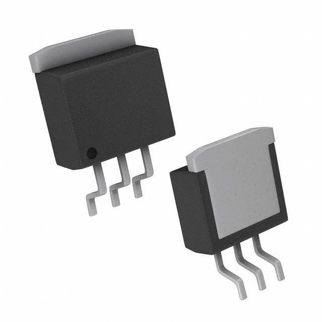
ICGOO电子元器件商城为您提供SPX1587AT-L-3-3由Exar设计生产,在icgoo商城现货销售,并且可以通过原厂、代理商等渠道进行代购。 SPX1587AT-L-3-3价格参考。ExarSPX1587AT-L-3-3封装/规格:PMIC - 稳压器 - 线性, Linear Voltage Regulator IC Positive Fixed 1 Output 3.3V 3A TO-263-3。您可以下载SPX1587AT-L-3-3参考资料、Datasheet数据手册功能说明书,资料中有SPX1587AT-L-3-3 详细功能的应用电路图电压和使用方法及教程。
| 参数 | 数值 |
| 产品目录 | 集成电路 (IC)半导体 |
| 描述 | IC REG LDO 3.3V 3A TO263-3低压差稳压器 3A LOW DROPOUT |
| 产品分类 | |
| 品牌 | Exar |
| 产品手册 | http://www.exar.com/power/power-conversion/ldos-and-regulators/linear-ldos/SPX1587/ |
| 产品图片 |
|
| rohs | 符合RoHS无铅 / 符合限制有害物质指令(RoHS)规范要求 |
| 产品系列 | 电源管理 IC,低压差稳压器,Exar SPX1587AT-L-3-3- |
| 数据手册 | http://www.exar.com/Common/Content/Document.ashx?id=601 |
| 产品型号 | SPX1587AT-L-3-3 |
| PSRR/纹波抑制—典型值 | 75 dB at 120 Hz |
| 产品种类 | 低压差稳压器 |
| 供应商器件封装 | TO-263-3 |
| 其它名称 | 1016-1241-5 |
| 包装 | 管件 |
| 商标 | Exar |
| 回动电压—最大值 | 1.2 V |
| 安装类型 | 表面贴装 |
| 安装风格 | SMD/SMT |
| 封装/外壳 | TO-263-4,D²Pak(3 引线+接片),TO-263AA |
| 封装/箱体 | TO-263-3 |
| 工作温度 | -40°C ~ 125°C |
| 工厂包装数量 | 50 |
| 最大工作温度 | + 125 C |
| 最大输入电压 | 10 V |
| 最小工作温度 | - 40 C |
| 最小输入电压 | 2.5 V |
| 标准包装 | 50 |
| 电压-跌落(典型值) | 1.1V @ 3A |
| 电压-输入 | 最高 10V |
| 电压-输出 | 3.3V |
| 电流-输出 | 3A |
| 电流-限制(最小值) | 3.2A |
| 稳压器拓扑 | 正,固定式 |
| 稳压器数 | 1 |
| 线路调整率 | 0.2 % |
| 负载调节 | 0.3 % |
| 输出电压 | 3.3 V |
| 输出电流 | 3 A |
| 输出端数量 | 1 Output |
| 输出类型 | Fixed |


PDF Datasheet 数据手册内容提取
SSPPXX11558877 33AA LLooww DDrrooppoouutt VVoollttaaggee RReegguullaattoorr September 2010 Rev. 2.0.0 GENERAL DESCRIPTION APPLICATIONS The SPX1587 is a low power positive-voltage • Desktop PC's Servers regulator designed to satisfy moderate power • Powering VGA and Sound Cards requirements with a cost effective, small footprint solution. • Adjustable Power Supplies This device is an excellent choice for use in • Portable Instrumentation battery-powered applications and portable computers. The SPX1587 features very low FEATURES quiescent current and a low dropout voltage of 1.1V at a full load. As output current • Guaranteed 3A Output Current decreases, quiescent current flows into the • Three Terminal Adjustable or Fixed load, increasing efficiency. SPX1587 is 1.5V, 2.5V, 3.3V and 5.0V available in adjustable or fixed 1.5V, 2.5V, 3.3V and 5.0V output voltages. • Low Quiescent Current The SPX1587 is offered in several 3-pin • Low Dropout Voltage: 1.1V at 3A surface mount packages: TO-252, TO-220 and • Line Regulation: 0.1% TO-263. An output capacitor of 10μF ceramic or tantalum provides unconditional stability. • Load Regulation: 0.1% • Stable with 10uF Ceramic Capacitor • Over Current and Thermal Protection • Similar to Industry Standard LT1085/LT1585 • RoHS Compliant Lead Free 3-Pin TO-220, TO-252 and TO-263 Packages FUNCTIONAL DIAGRAM Fig. 1: SPX1587 Functional Diagram (Adjustable version) Exar Corporation www.exar.com 48720 Kato Road, Fremont CA 94538, USA Tel. +1 510 668-7000 – Fax. +1 510 668-7001
SSPPXX11558877 33AA LLooww DDrrooppoouutt VVoollttaaggee RReegguullaattoorr ABSOLUTE MAXIMUM RATINGS OPERATING RATINGS These are stress ratings only and functional operation of Junction Temperature Range .................... -40°C to 125°C the device at these ratings or any other above those Thermal Resistance indicated in the operation sections of the specifications TO-220 θ ...................................................... 3°C/W below is not implied. Exposure to absolute maximum JC TO-220 θ ................................................. 29.4°C/W rating conditions for extended periods of time may affect JA reliability. TO-263 θJC ...................................................... 3°C/W TO-263 θ ................................................. 31.4°C/W Input Supply Voltage V .................................... +10.0V JA IN TO-252 θ ...................................................... 6°C/W Input to Output Voltage ....................................... +8.8V JC TO-252 θ .................................................... 50°C/W Storage Temperature .............................. -65°C to 150°C JA Power Dissipation ................................ Internally Limited Lead Temperature (Soldering, 5 sec) ..................... 260°C ESD Rating (HBM - Human Body Model) .................... 2kV ELECTRICAL SPECIFICATIONS Specifications with standard type are for an Operating Ambient Temperature of T = 25°C only; limits applying over the full A Operating Temperature range (-40°C to +85°C) are denoted by a “•”. Minimum and Maximum limits are guaranteed through test, design, or statistical correlation. Typical values represent the most likely parametric norm at T = 25°C, and A are provided for reference purposes only. Unless otherwise indicated, V = V + 1.5V, T = 25°C, C = C =10µF, IN OUT A IN OUT I =10mA. OUT Parameter Min. Typ. Max. Units Conditions 1.5V Version Output Voltage 1.485 1.500 1.515 V IOUT=10mA, VOUT=3.5V SPX1587A 1.470 1.530 • 10mA≤IOUT≤3A, 3.0V≤VOUT≤10V 2.5V Version Output Voltage 2.450 2.500 2.550 V IOUT=10mA, VOUT=4.5V SPX1587 2.425 2.575 • 10mA≤IOUT≤3A, 4.25V≤IOUT≤10V 3.3V Version Output Voltage 3.267 3.300 3.333 V IOUT=10mA, VOUT=5V SPX1587A 3.234 3.366 • 10mA≤IOUT≤3A, 4.75V≤VOUT≤10V Output Voltage 3.234 3.300 3.366 V IOUT=10mA, VOUT=5V SPX1587 3.201 3.399 • 10mA≤IOUT≤3A, 4.75V≤VOUT≤10V 5.0V Version Output Voltage 4.950 5.000 5.050 V IOUT=10mA, VOUT=7V SPX1587A 4.900 5.100 • 10mA≤IOUT≤3A, 6.50V≤VOUT≤10V All Voltage Options Reference Voltage 1.238 1.250 1.262 V IOUT=10mA, VIN-VOUT=2V SPX1587A 1.225 1.275 • 10mA≤IOUT≤3A, 1.50V≤VIN-VOUT≤10V Reference Voltage 1.225 1.250 1.275 V IOUT=10mA, VIN-VOUT=2V SPX1587 1.212 1.287 • 10mA≤IOUT≤3A, 1.50V≤VIN-VOUT≤10V Output Voltage Temperature 0.3 % Stability – SPX1587A Output Voltage Temperature 0.5 % Stability – SPX1587 3.0V≤V ≤10V, V =1.5V IN OUT 4.25V≤V ≤10V, V =2.5V Line Regulation 0.1 0.2 % IN OUT 4.75V≤V ≤10V, V =3.3V IN OUT 6.50V≤V ≤10V, V =5.0V IN OUT 10mA≤I ≤3A, V =1.5V OUT OUT 10mA≤I ≤3A, V =2.5V Load Regulation 0.1 0.3 % OUT OUT 10mA≤I ≤3A, V =3.3V OUT OUT 10mA≤I ≤3A, V =5.0V OUT OUT © 2010 Exar Corporation 2/11 Rev. 2.0.0
SSPPXX11558877 33AA LLooww DDrrooppoouutt VVoollttaaggee RReegguullaattoorr Parameter Min. Typ. Max. Units Conditions 1.00 IOUT=1A Dropout Voltage (note 2) 1.05 V IOUT=2A 1.10 1.2 IOUT=3A Minimum Load Current 4 10 mA (note 4) Quiescent Current 4 10 mA Fixed Voltage Versions 50 µA Adjust Pin Current 120 µA • Current Limit 3.2 5 A VIN-VOUT=2V Thermal Regulation 0.01 0.1 %/W 25°C, 30ms pulse Ripple Rejection 60 75 dB FRIPPLE=120Hz, VIN-VOUT=2V, VRIPPLE=1VPP Long Term Stability 0.03 % 125°C, 1000 hours RMS Output Noise 0.03 % % of VOUT, 10Hz ≤ f ≤ 10kHz Note 1: Output temperature coefficient is defined as the worst case voltage change divided by the total temperature range Note 2: Dropout voltage is defined as the input to output differential at which the output voltage drops 100mV below its nominal value measured at 1V differential at very low values of programmed output voltage, the minimum input supply voltage of 2V (2.3V over temperature) must be taken into account. Note 3: Thermal regulation is defined as the change in output voltage at a time T after a change in power dissipation is applied. Excluding load or line regulation effect. Note 4: Adjustable Version Only. BLOCK DIAGRAM Fig. 2: SPX1587 Block Diagram © 2010 Exar Corporation 3/11 Rev. 2.0.0
SSPPXX11558877 33AA LLooww DDrrooppoouutt VVoollttaaggee RReegguullaattoorr PIN ASSIGNMENT Fig. 3: SPX1587 Pin Assignment PIN DESCRIPTION Name Pin Number Description ADJ/GND 1 Adjustable Voltage Pin or Ground signal for fixed voltage versions. VOUT 2 Output Voltage VIN 3 Input Voltage TAB TAB Tab is connected to VOUT (pin 2) for all packages ORDERING INFORMATION Junction Part Number Marking Package Packing Quantity Note 1 Temperature Range SPX1587T-L Sipex Bulk -40°C≤T≤+125°C SPX1587T TO263-3 Lead Free SPX1587T-L/TR J 500/Tape & Reel YYWWLX SPX1587T-L-1-5 Sipex Bulk -40°C≤T≤+125°C SPX1587T TO263-3 Lead Free SPX1587T-L-1-5/TR J 500/Tape & Reel 15YYWWLX SPX1587T-L-5-0 Sipex Bulk -40°C≤T≤+125°C SPX1587T TO263-3 Lead Free SPX1587T-L-5-0/TR J 500/Tape & Reel 50YYWWLX Sipex SPX1587U-L-3-3 -40°C≤T≤+125°C SPX1587U TO220-3 Bulk Lead Free J 33YYWWLX Sipex SPX1587U-L-5-0 -40°C≤T≤+125°C SPX1587U TO220-3 Bulk Lead Free J 50YYWWLX SPX1587AR-L Sipex Bulk -40°C≤T≤+125°C SPX1587AR TO252-3 Lead Free SPX1587AR-L/TR J 2K/Tape & Reel YYWWLX SPX1587AT-L Sipex Bulk -40°C≤T≤+125°C SPX1587AT TO263-3 Lead Free SPX1587AT-L/TR J 500/Tape & Reel YYWWLX SPX1587AT-L-2-5 Sipex Bulk -40°C≤T≤+125°C SPX1587AT TO263-3 Lead Free SPX1587AT-L-2-5/TR J 500/Tape & Reel 25YYWWLX SPX1587AT-L-3-3 Sipex Bulk -40°C≤T≤+125°C SPX1587AT TO263-3 Lead Free SPX1587AT-L-3-3/TR J 500/Tape & Reel 33YYWWLX Sipex SPX1587AU-L -40°C≤T≤+125°C SPX1587AU TO220-3 Bulk Lead Free J YYWWLX “YY” = Year – “WW” = Work Week – “L” = Lead Free Indicator – “X” = Lot Number; when applicable. © 2010 Exar Corporation 4/11 Rev. 2.0.0
SSPPXX11558877 33AA LLooww DDrrooppoouutt VVoollttaaggee RReegguullaattoorr TYPICAL PERFORMANCE CHARACTERISTICS All data taken at V = V + 1.5V, T = 25°C, C = C =10µF, I =10mA unless otherwise specified - Schematic and IN OUT A IN OUT OUT BOM from Application Information section of this datasheet. Fig. 4: Line Regulation for SPX1587U-3-3 Fig. 5: V versus Temperature OUT I =10mA V =2.5V, I =10mA OUT IN OUT Fig. 6: VOUT versus Temperature Fig. 7: VOUT versus Temperature VIN=4.0V, IOUT=10mA VIN=5.0V, IOUT=10mA SOLDERING METHODS APPLICATION INFORMATION The SPX1587 die is attached to the heatsink OUTPUT CAPACITOR lead which exits opposite the input, output, and ground pins. To ensure the stability of the SPX1587, an output capacitor of at least 10μF (ceramic or THERMAL CHARACTERISTICS tantalum) or 22μF (aluminum) is required. The value may change based on the application The SPX1587 features the internal thermal requirements of the output load or limiting to protect the device during overload temperature range. The value of ESR can vary conditions. Special care needs to be taken based on the type of capacitor used in the during continuous load conditions such that applications to guarantee stability. The the maximum junction temperature does not recommended value for ESR is 0.5Ω or less. A exceed 125°C. Thermal protection is activated larger value of output capacitance (up to at >179°C and deactivated at <165 °C. 100μF) can improve the load transient The thermal interaction from other response. components in the application can affect the © 2010 Exar Corporation 5/11 Rev. 2.0.0
SSPPXX11558877 33AA LLooww DDrrooppoouutt VVoollttaaggee RReegguullaattoorr thermal resistance of the SPX1587. The actual If an ADJ-bypass capacitor is used, the thermal resistance can be determined with amplitude of the output ripple will be experimentation. independent of the output voltage. If an ADJ- bypass capacitor is not used, the output ripple The SPX1587 power dissipation is calculated will be proportional to the ratio of the output as follows: voltage to the reference voltage: (cid:1842) (cid:3404)(cid:4666)(cid:1848) (cid:3398)(cid:1848) (cid:4667)(cid:3400)(cid:1835) (cid:3005) (cid:3010)(cid:3015) (cid:3016)(cid:3022)(cid:3021) (cid:3016)(cid:3022)(cid:3021) (cid:1848) (cid:3016)(cid:3022)(cid:3021) (cid:1839) (cid:3404) (cid:1848) (cid:3019)(cid:3006)(cid:3007) Maximum Junction Temperature range: Where (cid:1846) (cid:3404)(cid:1846) (cid:3397)(cid:1842) (cid:3400)(cid:2016) M = multiplier for the ripple seen when the (cid:3011) (cid:3002)(cid:4666)(cid:3014)(cid:3002)(cid:3025)(cid:4667) (cid:3005) (cid:3011)(cid:3002) ADJ pin is optimally bypassed. V =1.25V Where θ is the junction-to-ambient thermal REF JA resistance of the package. Ripple rejection for the adjustable version is showing in Figure 8. Maximum junction temperature must not exceed 125°C. OUTPUT VOLTAGE RIPPLE REJECTION The output of the adjustable regulator can be set to any voltage between 1.25V and 15V. Ripple rejection can be improved by adding a The value of V can be quickly approximated capacitor between the ADJ pin and ground as OUT using the formula shown in Figure 11. When ADJ pin bypassing is used, the value of the output capacitor (cid:1844)(cid:2869)(cid:3397)(cid:1844)(cid:2870) (cid:1848) (cid:3404)1.25(cid:3400) required increases to its maximum. If the ADJ (cid:3016)(cid:3022)(cid:3021) (cid:1844) (cid:2869) pin is not bypassed, the value of the output Small correction to this formula is required de- capacitor can be lowered to 22μF for an pending on the values of resistors R1 and R2, electrolytic aluminum capacitor or 10μF for a since the adjustable pin current (approx 50μA) solid tantalum capacitor (Fig 10). flows through R2. When I is taken into ADJ However the value of the ADJ-bypass account, the formula becomes capacitor should be chosen with respect to the (cid:1844) (cid:2870) following equation: (cid:1848) (cid:3404)(cid:1848) (cid:3400)(cid:3436)1(cid:3397) (cid:3440)(cid:3397)(cid:1835) (cid:3400)(cid:1844) (cid:3016)(cid:3022)(cid:3021) (cid:3019)(cid:3006)(cid:3007) (cid:1844) (cid:3002)(cid:3005)(cid:3011) (cid:2870) (cid:2869) 1 (cid:1829) (cid:3404) Where 6.28(cid:3400)(cid:1832) (cid:3400)(cid:1844) (cid:3019) (cid:2869) V =1.25V REF Where LAYOUT CONSIDERATIONS C = value of the capacitor in Farads (select an Parasitic line resistance can degrade load equal or larger standard value) regulation. In order to avoid this, connect R1 directly to V as illustrated in Figure 13. For F = ripple frequency in Hz OUT R the same reason, R2 should be connected to R = value of resistor R1 in Ohms. the negative side of the load. 1 © 2010 Exar Corporation 6/11 Rev. 2.0.0
SSPPXX11558877 33AA LLooww DDrrooppoouutt VVoollttaaggee RReegguullaattoorr Fig. 8: Ripple Rejection Fig. 9: Current Source VIN=3.3V, VOUT=1.8V(adj), ILOAD=200mA Fig. 10: Typical Adjustable Regulator Fig. 11: Improving Ripple Rejection Fig. 12: 5V Regulator With Shutdown Fig. 13: Recommended Connections for Best Results © 2010 Exar Corporation 7/11 Rev. 2.0.0
SSPPXX11558877 33AA LLooww DDrrooppoouutt VVoollttaaggee RReegguullaattoorr PACKAGE SPECIFICATION 3-PIN TO263 © 2010 Exar Corporation 8/11 Rev. 2.0.0
SSPPXX11558877 33AA LLooww DDrrooppoouutt VVoollttaaggee RReegguullaattoorr 3-PIN TO220 © 2010 Exar Corporation 9/11 Rev. 2.0.0
SSPPXX11558877 33AA LLooww DDrrooppoouutt VVoollttaaggee RReegguullaattoorr 3-PIN TO252 © 2010 Exar Corporation 10/11 Rev. 2.0.0
SSPPXX11558877 33AA LLooww DDrrooppoouutt VVoollttaaggee RReegguullaattoorr REVISION HISTORY Revision Date Description Reformat of datasheet 2.0.0 Added marking information FOR FURTHER ASSISTANCE Email: customersupport@exar.com Exar Technical Documentation: http://www.exar.com/TechDoc/default.aspx? EXAR CORPORATION HEADQUARTERS AND SALES OFFICES 48720 Kato Road Fremont, CA 94538 – USA Tel.: +1 (510) 668-7000 Fax: +1 (510) 668-7030 www.exar.com NOTICE EXAR Corporation reserves the right to make changes to the products contained in this publication in order to improve design, performance or reliability. EXAR Corporation assumes no responsibility for the use of any circuits described herein, conveys no license under any patent or other right, and makes no representation that the circuits are free of patent infringement. Charts and schedules contained here in are only for illustration purposes and may vary depending upon a user’s specific application. While the information in this publication has been carefully checked; no responsibility, however, is assumed for inaccuracies. EXAR Corporation does not recommend the use of any of its products in life support applications where the failure or malfunction of the product can reasonably be expected to cause failure of the life support system or to significantly affect its safety or effectiveness. Products are not authorized for use in such applications unless EXAR Corporation receives, in writing, assurances to its satisfaction that: (a) the risk of injury or damage has been minimized; (b) the user assumes all such risks; (c) potential liability of EXAR Corporation is adequately protected under the circumstances. Reproduction, in part or whole, without the prior written consent of EXAR Corporation is prohibited. © 2010 Exar Corporation 11/11 Rev. 2.0.0

 Datasheet下载


