ICGOO在线商城 > 集成电路(IC) > 嵌入式 - 微控制器 > SPC56EL70L5CBFR

 Datasheet下载
- 型号: SPC56EL70L5CBFR
- 制造商: STMicroelectronics
- 库位|库存: xxxx|xxxx
- 要求:
| 数量阶梯 | 香港交货 | 国内含税 |
| +xxxx | $xxxx | ¥xxxx |
查看当月历史价格
查看今年历史价格
SPC56EL70L5CBFR产品简介:
ICGOO电子元器件商城为您提供SPC56EL70L5CBFR由STMicroelectronics设计生产,在icgoo商城现货销售,并且可以通过原厂、代理商等渠道进行代购。 SPC56EL70L5CBFR价格参考。STMicroelectronicsSPC56EL70L5CBFR封装/规格:嵌入式 - 微控制器, e200z4d 微控制器 IC SPC56xL 32 位双核 120MHz 2MB(2M x 8) 闪存 144-LQFP(20x20)。您可以下载SPC56EL70L5CBFR参考资料、Datasheet数据手册功能说明书,资料中有SPC56EL70L5CBFR 详细功能的应用电路图电压和使用方法及教程。
| 参数 | 数值 |
| 产品目录 | 集成电路 (IC) |
| 描述 | IC MCU 32BIT 2MB FLASH 144LQFP |
| EEPROM容量 | - |
| 产品分类 | |
| I/O数 | 96 |
| 品牌 | STMicroelectronics |
| 数据手册 | |
| 产品图片 |
|
| 产品型号 | SPC56EL70L5CBFR |
| RAM容量 | 192K x 8 |
| rohs | 无铅 / 符合限制有害物质指令(RoHS)规范要求 |
| 产品系列 | SPC56xL |
| 供应商器件封装 | * |
| 其它名称 | 497-13568-1 |
| 其它有关文件 | http://www.st.com/web/catalog/sense_power/FM2098/SC963/SS1534/PF252000?referrer=70071840 |
| 包装 | 剪切带 (CT) |
| 外设 | DMA,LVD,POR,PWM,WDT |
| 封装/外壳 | 144-LQFP |
| 工作温度 | -40°C ~ 125°C |
| 振荡器类型 | 内部 |
| 数据转换器 | A/D 32x12b |
| 标准包装 | 1 |
| 核心处理器 | e200z4d |
| 核心尺寸 | 32 位双核 |
| 电压-电源(Vcc/Vdd) | 3 V ~ 3.63 V |
| 程序存储器类型 | 闪存 |
| 程序存储容量 | 2MB(2M x 8) |
| 连接性 | CAN,LIN,SCI,SPI,UART/USART |
| 速度 | 120MHz |


- 商务部:美国ITC正式对集成电路等产品启动337调查
- 曝三星4nm工艺存在良率问题 高通将骁龙8 Gen1或转产台积电
- 太阳诱电将投资9.5亿元在常州建新厂生产MLCC 预计2023年完工
- 英特尔发布欧洲新工厂建设计划 深化IDM 2.0 战略
- 台积电先进制程称霸业界 有大客户加持明年业绩稳了
- 达到5530亿美元!SIA预计今年全球半导体销售额将创下新高
- 英特尔拟将自动驾驶子公司Mobileye上市 估值或超500亿美元
- 三星加码芯片和SET,合并消费电子和移动部门,撤换高东真等 CEO
- 三星电子宣布重大人事变动 还合并消费电子和移动部门
- 海关总署:前11个月进口集成电路产品价值2.52万亿元 增长14.8%


PDF Datasheet 数据手册内容提取
SPC56EL70L3, SPC56EL70L5, SPC564L70L3, SPC564L70L5 ® 32-bit Power Architecture microcontroller for automotive SIL3/ASILD chassis and safety applications Datasheet - production data – Replicated junction temperature sensor – Non Maskable Interrupt (NMI) – 16-region Memory Protection Unit (MPU) – Clock Monitoring Units (CMU) – Power Management Unit (PMU) – Cyclic Redundancy Check (CRC) unit LQFP144 (20 x 20 x 1.4 mm) LQFP100 (14 x 14x 1.4 mm) Decoupled Parallel mode for high performance use of replicated cores Features Nexus Class 3+ interface High-performance e200z4d dual core Interrupts – 32-bit Power Architecture® technology – Replicated 16-priority controller CPU – Replicated 16-channel eDMA controller – Core frequency as high as 120 MHz GPIOs individually programmable as input, – Dual issue five-stage pipeline core output or special function – Variable Length Encoding (VLE) Three 6-channel general-purpose eTimer units – Memory Management Unit (MMU) 2 FlexPWM units: Four 16-bit channels per – 4 KB instruction cache with error detection module code Communications interfaces – Signal Processing Engine (SPE) – 2 LINFlexD channels Memory available – 3 DSPI channels with automatic chip select – 2 MB flash memory with ECC generation – 192 KB on-chip SRAM with ECC – 3 FlexCAN interfaces (2.0B Active) with 32 – Built-in RWW capabilities for EEPROM message objects emulation – FlexRay module (V2.1 Rev. A) with 2 SIL3/ASILD innovative safety concept: Lock channels, 64 message buffers and data step mode and Fail-safe protection rates up to 10 Mbit/s – Sphere of Replication (SoR) for key Two 12-bit Analog-to-digital Converters (ADC) components (such as CPU core, eDMA, – 16 input channels crossbar switch) – Programmable Cross Triggering Unit (CTU) – Fault Collection and Control Unit (FCCU) to synchronize ADCs conversion with timer – Redundancy Control and Checker Unit and PWM (RCCU) on outputs of the SoR connected Sine wave generator (D/A with low pass filter) to FCCU On-chip CAN/UART/FlexRay Bootstrap loader – Boot-time Built-In Self-Test for Memory (MBIST) and Logic (LBIST) triggered by Single 3.0 V to 3.6 V voltage supply hardware Ambient temperature range –40 °C to 125 °C – Boot-time Built-In Self-Test for ADC and Junction temperature range –40 °C to 150 °C flash memory triggered by software – Replicated safety enhanced watchdog July 2015 DocID023953 Rev 5 1/128 This is information on a product in full production. www.st.com
Contents SPC56EL70L3, SPC56EL70L5,PC564L70L3, SPC564L70L5 Contents 1 Introduction . . . . . . . . . . . . . . . . . . . . . . . . . . . . . . . . . . . . . . . . . . . . . . . . 7 1.1 Document overview . . . . . . . . . . . . . . . . . . . . . . . . . . . . . . . . . . . . . . . . . . 7 1.2 Description . . . . . . . . . . . . . . . . . . . . . . . . . . . . . . . . . . . . . . . . . . . . . . . . . 7 1.3 Device comparison . . . . . . . . . . . . . . . . . . . . . . . . . . . . . . . . . . . . . . . . . . . 8 1.4 Block diagram . . . . . . . . . . . . . . . . . . . . . . . . . . . . . . . . . . . . . . . . . . . . . . .11 1.5 Feature details . . . . . . . . . . . . . . . . . . . . . . . . . . . . . . . . . . . . . . . . . . . . . 12 1.5.1 High-performance e200z4d core . . . . . . . . . . . . . . . . . . . . . . . . . . . . . . 12 1.5.2 Crossbar switch (XBAR) . . . . . . . . . . . . . . . . . . . . . . . . . . . . . . . . . . . . 13 1.5.3 Memory protection unit (MPU) . . . . . . . . . . . . . . . . . . . . . . . . . . . . . . . . 13 1.5.4 Enhanced direct memory access (eDMA) . . . . . . . . . . . . . . . . . . . . . . . 13 1.5.5 On-chip flash memory with ECC . . . . . . . . . . . . . . . . . . . . . . . . . . . . . . 14 1.5.6 On-chip SRAM with ECC . . . . . . . . . . . . . . . . . . . . . . . . . . . . . . . . . . . . 14 1.5.7 Platform flash memory controller . . . . . . . . . . . . . . . . . . . . . . . . . . . . . . 15 1.5.8 Platform static RAM controller (SRAMC) . . . . . . . . . . . . . . . . . . . . . . . . 15 1.5.9 Memory subsystem access time . . . . . . . . . . . . . . . . . . . . . . . . . . . . . . 16 1.5.10 Error correction status module (ECSM) . . . . . . . . . . . . . . . . . . . . . . . . . 16 1.5.11 Peripheral bridge (PBRIDGE) . . . . . . . . . . . . . . . . . . . . . . . . . . . . . . . . 17 1.5.12 Interrupt controller (INTC) . . . . . . . . . . . . . . . . . . . . . . . . . . . . . . . . . . . 17 1.5.13 System clocks and clock generation . . . . . . . . . . . . . . . . . . . . . . . . . . . 18 1.5.14 Frequency-Modulated Phase-Locked Loop (FMPLL) . . . . . . . . . . . . . . 18 1.5.15 Main oscillator . . . . . . . . . . . . . . . . . . . . . . . . . . . . . . . . . . . . . . . . . . . . 19 1.5.16 Internal reference clock (RC) oscillator . . . . . . . . . . . . . . . . . . . . . . . . . 19 1.5.17 Clock, reset, power, mode and test control modules (MC_CGM, MC_RGM, MC_PCU, and MC_ME) . . . . . . . . . . . . . . . . . . . . . . . . . . . 19 1.5.18 Periodic interrupt timer module (PIT) . . . . . . . . . . . . . . . . . . . . . . . . . . . 19 1.5.19 System timer module (STM) . . . . . . . . . . . . . . . . . . . . . . . . . . . . . . . . . 20 1.5.20 Software watchdog timer (SWT) . . . . . . . . . . . . . . . . . . . . . . . . . . . . . . 20 1.5.21 Fault collection and control unit (FCCU) . . . . . . . . . . . . . . . . . . . . . . . . 20 1.5.22 System Integration Unit Lite (SIUL) . . . . . . . . . . . . . . . . . . . . . . . . . . . . 20 1.5.23 Non-maskable interrupt (NMI) . . . . . . . . . . . . . . . . . . . . . . . . . . . . . . . . 21 1.5.24 Boot assist module (BAM) . . . . . . . . . . . . . . . . . . . . . . . . . . . . . . . . . . . 21 1.5.25 System status and configuration module (SSCM) . . . . . . . . . . . . . . . . . 21 1.5.26 FlexCAN . . . . . . . . . . . . . . . . . . . . . . . . . . . . . . . . . . . . . . . . . . . . . . . . 21 1.5.27 FlexRay . . . . . . . . . . . . . . . . . . . . . . . . . . . . . . . . . . . . . . . . . . . . . . . . . 23 2/128 DocID023953 Rev 5
SPC56EL70L3, SPC56EL70L5,PC564L70L3, SPC564L70L5 Contents 1.5.28 Serial communication interface module (LINFlexD) . . . . . . . . . . . . . . . 24 1.5.29 Deserial serial peripheral interface (DSPI) . . . . . . . . . . . . . . . . . . . . . . 25 1.5.30 FlexPWM . . . . . . . . . . . . . . . . . . . . . . . . . . . . . . . . . . . . . . . . . . . . . . . . 25 1.5.31 eTimer module . . . . . . . . . . . . . . . . . . . . . . . . . . . . . . . . . . . . . . . . . . . . 27 1.5.32 Sine wave generator (SWG) . . . . . . . . . . . . . . . . . . . . . . . . . . . . . . . . . 27 1.5.33 Analog-to-Digital converter module (ADC) . . . . . . . . . . . . . . . . . . . . . . 28 1.5.34 Cross triggering unit (CTU) . . . . . . . . . . . . . . . . . . . . . . . . . . . . . . . . . . 28 1.5.35 Cyclic redundancy checker (CRC) unit . . . . . . . . . . . . . . . . . . . . . . . . . 29 1.5.36 Redundancy control and checker unit (RCCU) . . . . . . . . . . . . . . . . . . . 29 1.5.37 Junction temperature sensor . . . . . . . . . . . . . . . . . . . . . . . . . . . . . . . . . 30 1.5.38 Nexus port controller (NPC) . . . . . . . . . . . . . . . . . . . . . . . . . . . . . . . . . . 30 1.5.39 IEEE 1149.1 JTAG controller (JTAGC) . . . . . . . . . . . . . . . . . . . . . . . . . 31 1.5.40 Voltage regulator / power management unit (PMU) . . . . . . . . . . . . . . . . 31 1.5.41 Built-In self-test (BIST) capability . . . . . . . . . . . . . . . . . . . . . . . . . . . . . . 32 2 Package pinouts and signal descriptions . . . . . . . . . . . . . . . . . . . . . . . 33 2.1 Package pinouts . . . . . . . . . . . . . . . . . . . . . . . . . . . . . . . . . . . . . . . . . . . . 33 2.2 Supply pins . . . . . . . . . . . . . . . . . . . . . . . . . . . . . . . . . . . . . . . . . . . . . . . . 54 2.3 System pins . . . . . . . . . . . . . . . . . . . . . . . . . . . . . . . . . . . . . . . . . . . . . . . 56 2.4 Pin muxing . . . . . . . . . . . . . . . . . . . . . . . . . . . . . . . . . . . . . . . . . . . . . . . . 57 3 Electrical characteristics . . . . . . . . . . . . . . . . . . . . . . . . . . . . . . . . . . . . 74 3.1 Introduction . . . . . . . . . . . . . . . . . . . . . . . . . . . . . . . . . . . . . . . . . . . . . . . 74 3.2 Absolute maximum ratings . . . . . . . . . . . . . . . . . . . . . . . . . . . . . . . . . . . . 74 3.3 Recommended operating conditions . . . . . . . . . . . . . . . . . . . . . . . . . . . . 75 3.4 Decoupling capacitors . . . . . . . . . . . . . . . . . . . . . . . . . . . . . . . . . . . . . . . 76 3.5 Thermal characteristics . . . . . . . . . . . . . . . . . . . . . . . . . . . . . . . . . . . . . . 79 3.5.1 General notes for specifications at maximum junction temperature . . . 79 3.6 Electromagnetic Interference (EMI) characteristics . . . . . . . . . . . . . . . . . 81 3.7 Electrostatic discharge (ESD) characteristics . . . . . . . . . . . . . . . . . . . . . 82 3.8 Static latch-up (LU) . . . . . . . . . . . . . . . . . . . . . . . . . . . . . . . . . . . . . . . . . . 83 3.9 Voltage regulator electrical characteristics . . . . . . . . . . . . . . . . . . . . . . . . 83 3.10 Supply current characteristics . . . . . . . . . . . . . . . . . . . . . . . . . . . . . . . . . 87 3.11 Temperature sensor electrical characteristics . . . . . . . . . . . . . . . . . . . . . 90 3.12 Main oscillator electrical characteristics . . . . . . . . . . . . . . . . . . . . . . . . . . 90 DocID023953 Rev 5 3/128 4
Contents SPC56EL70L3, SPC56EL70L5,PC564L70L3, SPC564L70L5 3.13 FMPLL electrical characteristics . . . . . . . . . . . . . . . . . . . . . . . . . . . . . . . . 92 3.14 16 MHz RC oscillator electrical characteristics . . . . . . . . . . . . . . . . . . . . 93 3.15 ADC electrical characteristics . . . . . . . . . . . . . . . . . . . . . . . . . . . . . . . . . . 93 3.15.1 Input Impedance and ADC Accuracy . . . . . . . . . . . . . . . . . . . . . . . . . . . 94 3.16 Flash memory electrical characteristics . . . . . . . . . . . . . . . . . . . . . . . . . . 99 3.17 SWG electrical characteristics . . . . . . . . . . . . . . . . . . . . . . . . . . . . . . . . 101 3.18 AC specifications . . . . . . . . . . . . . . . . . . . . . . . . . . . . . . . . . . . . . . . . . . 101 3.18.1 Pad AC specifications . . . . . . . . . . . . . . . . . . . . . . . . . . . . . . . . . . . . . 101 3.19 Reset sequence . . . . . . . . . . . . . . . . . . . . . . . . . . . . . . . . . . . . . . . . . . . 102 3.19.1 Reset sequence duration . . . . . . . . . . . . . . . . . . . . . . . . . . . . . . . . . . . 102 3.19.2 Reset sequence description . . . . . . . . . . . . . . . . . . . . . . . . . . . . . . . . 103 3.19.3 Reset sequence trigger mapping . . . . . . . . . . . . . . . . . . . . . . . . . . . . . 105 3.19.4 Reset sequence — start condition . . . . . . . . . . . . . . . . . . . . . . . . . . . . 106 3.19.5 External watchdog window . . . . . . . . . . . . . . . . . . . . . . . . . . . . . . . . . 108 3.20 AC timing characteristics . . . . . . . . . . . . . . . . . . . . . . . . . . . . . . . . . . . . 108 3.20.1 RESET pin characteristics . . . . . . . . . . . . . . . . . . . . . . . . . . . . . . . . . . 108 3.20.2 WKUP/NMI timing . . . . . . . . . . . . . . . . . . . . . . . . . . . . . . . . . . . . . . . . 110 3.20.3 IEEE 1149.1 JTAG interface timing . . . . . . . . . . . . . . . . . . . . . . . . . . . 110 3.20.4 Nexus timing . . . . . . . . . . . . . . . . . . . . . . . . . . . . . . . . . . . . . . . . . . . . 112 3.20.5 External interrupt timing (IRQ pin) . . . . . . . . . . . . . . . . . . . . . . . . . . . . 114 3.20.6 DSPI timing . . . . . . . . . . . . . . . . . . . . . . . . . . . . . . . . . . . . . . . . . . . . . 115 4 Package characteristics . . . . . . . . . . . . . . . . . . . . . . . . . . . . . . . . . . . . 121 4.1 ECOPACK® . . . . . . . . . . . . . . . . . . . . . . . . . . . . . . . . . . . . . . . . . . . . . . 121 4.2 Package mechanical data . . . . . . . . . . . . . . . . . . . . . . . . . . . . . . . . . . . 121 5 Ordering information . . . . . . . . . . . . . . . . . . . . . . . . . . . . . . . . . . . . . . 125 6 Revision history . . . . . . . . . . . . . . . . . . . . . . . . . . . . . . . . . . . . . . . . . . 126 4/128 DocID023953 Rev 5
SPC56EL70L3, SPC56EL70L5,PC564L70L3, SPC564L70L5 List of tables List of tables Table 1. SPC56XL70/SPC56X64 device summary . . . . . . . . . . . . . . . . . . . . . . . . . . . . . . . . . . . . . . 8 Table 2. Platform memory access time summary. . . . . . . . . . . . . . . . . . . . . . . . . . . . . . . . . . . . . . . 16 Table 3. LQFP100 pin function summary. . . . . . . . . . . . . . . . . . . . . . . . . . . . . . . . . . . . . . . . . . . . . 34 Table 4. LQFP144 pin function summary. . . . . . . . . . . . . . . . . . . . . . . . . . . . . . . . . . . . . . . . . . . . . 42 Table 5. Supply pins. . . . . . . . . . . . . . . . . . . . . . . . . . . . . . . . . . . . . . . . . . . . . . . . . . . . . . . . . . . . . 54 Table 6. System pins . . . . . . . . . . . . . . . . . . . . . . . . . . . . . . . . . . . . . . . . . . . . . . . . . . . . . . . . . . . . 56 Table 7. Pin muxing . . . . . . . . . . . . . . . . . . . . . . . . . . . . . . . . . . . . . . . . . . . . . . . . . . . . . . . . . . . . . 57 Table 8. Absolute maximum ratings. . . . . . . . . . . . . . . . . . . . . . . . . . . . . . . . . . . . . . . . . . . . . . . . . 74 Table 9. Recommended operating conditions (3.3 V) . . . . . . . . . . . . . . . . . . . . . . . . . . . . . . . . . . . 75 Table 10. Decoupling capacitors . . . . . . . . . . . . . . . . . . . . . . . . . . . . . . . . . . . . . . . . . . . . . . . . . . . . 76 Table 11. Thermal characteristics for LQFP100 package . . . . . . . . . . . . . . . . . . . . . . . . . . . . . . . . . 79 Table 12. Thermal characteristics for LQFP144 package . . . . . . . . . . . . . . . . . . . . . . . . . . . . . . . . . 79 Table 13. EMI configuration summary . . . . . . . . . . . . . . . . . . . . . . . . . . . . . . . . . . . . . . . . . . . . . . . . 81 Table 14. EMI emission testing specifications . . . . . . . . . . . . . . . . . . . . . . . . . . . . . . . . . . . . . . . . . . 82 Table 15. ESD ratings. . . . . . . . . . . . . . . . . . . . . . . . . . . . . . . . . . . . . . . . . . . . . . . . . . . . . . . . . . . . . 82 Table 16. Latch-up results . . . . . . . . . . . . . . . . . . . . . . . . . . . . . . . . . . . . . . . . . . . . . . . . . . . . . . . . . 83 Table 17. Recommended operating characteristics. . . . . . . . . . . . . . . . . . . . . . . . . . . . . . . . . . . . . . 83 Table 18. Voltage regulator electrical specifications. . . . . . . . . . . . . . . . . . . . . . . . . . . . . . . . . . . . . . 84 Table 19. DC electrical characteristics. . . . . . . . . . . . . . . . . . . . . . . . . . . . . . . . . . . . . . . . . . . . . . . . 86 Table 20. Current consumption characteristics . . . . . . . . . . . . . . . . . . . . . . . . . . . . . . . . . . . . . . . . . 88 Table 21. Temperature sensor electrical characteristics . . . . . . . . . . . . . . . . . . . . . . . . . . . . . . . . . . 90 Table 22. Main oscillator electrical characteristics . . . . . . . . . . . . . . . . . . . . . . . . . . . . . . . . . . . . . . . 91 Table 23. FMPLL electrical characteristics. . . . . . . . . . . . . . . . . . . . . . . . . . . . . . . . . . . . . . . . . . . . . 92 Table 24. RC oscillator electrical characteristics . . . . . . . . . . . . . . . . . . . . . . . . . . . . . . . . . . . . . . . . 93 Table 25. ADC conversion characteristics . . . . . . . . . . . . . . . . . . . . . . . . . . . . . . . . . . . . . . . . . . . . . 98 Table 26. Flash memory program and erase electrical specifications . . . . . . . . . . . . . . . . . . . . . . . . 99 Table 27. Flash memory timing . . . . . . . . . . . . . . . . . . . . . . . . . . . . . . . . . . . . . . . . . . . . . . . . . . . . . 99 Table 28. Flash memory module life. . . . . . . . . . . . . . . . . . . . . . . . . . . . . . . . . . . . . . . . . . . . . . . . . 100 Table 29. SPC56XL70 SWG Specifications. . . . . . . . . . . . . . . . . . . . . . . . . . . . . . . . . . . . . . . . . . . 101 Table 30. Pad AC specifications (3.3 V, IPP_HVE = 0) . . . . . . . . . . . . . . . . . . . . . . . . . . . . . . . . . . 101 Table 31. RESET sequences. . . . . . . . . . . . . . . . . . . . . . . . . . . . . . . . . . . . . . . . . . . . . . . . . . . . . . 103 Table 32. Reset sequence trigger — Reset sequence. . . . . . . . . . . . . . . . . . . . . . . . . . . . . . . . . . . 105 Table 33. Voltage thresholds . . . . . . . . . . . . . . . . . . . . . . . . . . . . . . . . . . . . . . . . . . . . . . . . . . . . . . 107 Table 34. RESET electrical characteristics. . . . . . . . . . . . . . . . . . . . . . . . . . . . . . . . . . . . . . . . . . . . 109 Table 35. WKUP/NMI glitch filter . . . . . . . . . . . . . . . . . . . . . . . . . . . . . . . . . . . . . . . . . . . . . . . . . . . 110 Table 36. JTAG pin AC electrical characteristics . . . . . . . . . . . . . . . . . . . . . . . . . . . . . . . . . . . . . . . 110 Table 37. Nexus debug port timing. . . . . . . . . . . . . . . . . . . . . . . . . . . . . . . . . . . . . . . . . . . . . . . . . . 112 Table 38. External interrupt timing . . . . . . . . . . . . . . . . . . . . . . . . . . . . . . . . . . . . . . . . . . . . . . . . . . 114 Table 39. DSPI timing. . . . . . . . . . . . . . . . . . . . . . . . . . . . . . . . . . . . . . . . . . . . . . . . . . . . . . . . . . . . 115 Table 40. LQFP100 mechanical data. . . . . . . . . . . . . . . . . . . . . . . . . . . . . . . . . . . . . . . . . . . . . . . . 122 Table 41. LQFP144 mechanical data. . . . . . . . . . . . . . . . . . . . . . . . . . . . . . . . . . . . . . . . . . . . . . . . 123 Table 42. Revision history . . . . . . . . . . . . . . . . . . . . . . . . . . . . . . . . . . . . . . . . . . . . . . . . . . . . . . . . 126 DocID023953 Rev 5 5/128 5
List of figures SPC56EL70L3, SPC56EL70L5,PC564L70L3, SPC564L70L5 List of figures Figure 1. SPC56EL70 block diagram. . . . . . . . . . . . . . . . . . . . . . . . . . . . . . . . . . . . . . . . . . . . . . . . . 11 Figure 2. SPC56XL70 LQFP100 package. . . . . . . . . . . . . . . . . . . . . . . . . . . . . . . . . . . . . . . . . . . . . 33 Figure 3. SPC56XL70 LQFP144 pinout (top view) . . . . . . . . . . . . . . . . . . . . . . . . . . . . . . . . . . . . . . 34 Figure 4. Decoupling capacitors . . . . . . . . . . . . . . . . . . . . . . . . . . . . . . . . . . . . . . . . . . . . . . . . . . . . 78 Figure 5. BCP68 board schematic example . . . . . . . . . . . . . . . . . . . . . . . . . . . . . . . . . . . . . . . . . . . 86 Figure 6. Crystal oscillator and resonator connection scheme . . . . . . . . . . . . . . . . . . . . . . . . . . . . . 90 Figure 7. Main oscillator electrical characteristics . . . . . . . . . . . . . . . . . . . . . . . . . . . . . . . . . . . . . . . 91 Figure 8. ADC characteristics and error definitions. . . . . . . . . . . . . . . . . . . . . . . . . . . . . . . . . . . . . . 94 Figure 9. Input Equivalent Circuit. . . . . . . . . . . . . . . . . . . . . . . . . . . . . . . . . . . . . . . . . . . . . . . . . . . . 95 Figure 10. Transient Behavior during Sampling Phase. . . . . . . . . . . . . . . . . . . . . . . . . . . . . . . . . . . . 95 Figure 11. Spectral representation of input signal. . . . . . . . . . . . . . . . . . . . . . . . . . . . . . . . . . . . . . . . 97 Figure 12. Pad output delay. . . . . . . . . . . . . . . . . . . . . . . . . . . . . . . . . . . . . . . . . . . . . . . . . . . . . . . . 102 Figure 13. Destructive Reset Sequence, BIST enabled . . . . . . . . . . . . . . . . . . . . . . . . . . . . . . . . . . 103 Figure 14. Destructive Reset Sequence, BIST disabled . . . . . . . . . . . . . . . . . . . . . . . . . . . . . . . . . . 104 Figure 15. External Reset Sequence Long, BIST enabled . . . . . . . . . . . . . . . . . . . . . . . . . . . . . . . . 104 Figure 16. Functional Reset Sequence Long. . . . . . . . . . . . . . . . . . . . . . . . . . . . . . . . . . . . . . . . . . . 104 Figure 17. Functional Reset Sequence Short . . . . . . . . . . . . . . . . . . . . . . . . . . . . . . . . . . . . . . . . . . 105 Figure 18. Reset sequence start for destructive resets. . . . . . . . . . . . . . . . . . . . . . . . . . . . . . . . . . . 107 Figure 19. Reset sequence start via RESET assertion . . . . . . . . . . . . . . . . . . . . . . . . . . . . . . . . . . . 107 Figure 20. Reset sequence - External watchdog trigger window position . . . . . . . . . . . . . . . . . . . . . 108 Figure 21. Start-up reset requirements . . . . . . . . . . . . . . . . . . . . . . . . . . . . . . . . . . . . . . . . . . . . . . . 109 Figure 22. Noise filtering on reset signal . . . . . . . . . . . . . . . . . . . . . . . . . . . . . . . . . . . . . . . . . . . . . . 109 Figure 23. JTAG test clock input timing. . . . . . . . . . . . . . . . . . . . . . . . . . . . . . . . . . . . . . . . . . . . . . . 110 Figure 24. JTAG test access port timing . . . . . . . . . . . . . . . . . . . . . . . . . . . . . . . . . . . . . . . . . . . . . . 111 Figure 25. JTAG boundary scan timing. . . . . . . . . . . . . . . . . . . . . . . . . . . . . . . . . . . . . . . . . . . . . . . 112 Figure 26. Nexus output timing . . . . . . . . . . . . . . . . . . . . . . . . . . . . . . . . . . . . . . . . . . . . . . . . . . . . . 113 Figure 27. Nexus DDR Mode output timing. . . . . . . . . . . . . . . . . . . . . . . . . . . . . . . . . . . . . . . . . . . . 113 Figure 28. Nexus TDI, TMS, TDO timing. . . . . . . . . . . . . . . . . . . . . . . . . . . . . . . . . . . . . . . . . . . . . . 114 Figure 29. External interrupt timing . . . . . . . . . . . . . . . . . . . . . . . . . . . . . . . . . . . . . . . . . . . . . . . . . . 115 Figure 30. DSPI classic SPI timing — master, CPHA = 0 . . . . . . . . . . . . . . . . . . . . . . . . . . . . . . . . . 116 Figure 31. DSPI classic SPI timing — master, CPHA = 1 . . . . . . . . . . . . . . . . . . . . . . . . . . . . . . . . . 117 Figure 32. DSPI classic SPI timing — slave, CPHA = 0 . . . . . . . . . . . . . . . . . . . . . . . . . . . . . . . . . . 117 Figure 33. DSPI classic SPI timing — slave, CPHA = 1 . . . . . . . . . . . . . . . . . . . . . . . . . . . . . . . . . . 118 Figure 34. DSPI modified transfer format timing — master, CPHA = 0. . . . . . . . . . . . . . . . . . . . . . . 118 Figure 35. DSPI modified transfer format timing — master, CPHA = 1. . . . . . . . . . . . . . . . . . . . . . . 119 Figure 36. DSPI modified transfer format timing – slave, CPHA = 0. . . . . . . . . . . . . . . . . . . . . . . . . 119 Figure 37. DSPI modified transfer format timing — slave, CPHA = 1 . . . . . . . . . . . . . . . . . . . . . . . . 120 Figure 38. DSPI PCS strobe (PCSS) timing . . . . . . . . . . . . . . . . . . . . . . . . . . . . . . . . . . . . . . . . . . . 120 Figure 39. LQFP100 package mechanical drawing. . . . . . . . . . . . . . . . . . . . . . . . . . . . . . . . . . . . . . 121 Figure 40. LQFP144 package mechanical drawing. . . . . . . . . . . . . . . . . . . . . . . . . . . . . . . . . . . . . . 123 Figure 41. Commercial product code structure . . . . . . . . . . . . . . . . . . . . . . . . . . . . . . . . . . . . . . . . . 125 6/128 DocID023953 Rev 5
SPC56EL70L3, SPC56EL70L5,PC564L70L3, SPC564L70L5 Introduction 1 Introduction 1.1 Document overview This document describes the features of the family and options available within the family members, and highlights important electrical and physical characteristics of the devices. This document provides electrical specifications, pin assignments, and package diagrams for the SPC56EL70x/SPC564L70x series of microcontroller units (MCUs). For functional characteristics, see the SPC56XL70 Microcontroller Reference Manual. For use of the SPC56XL70 in a fail-safe system according to safety standard ISO26262, see the Safety Application Guide for SPCEL70. 1.2 Description The SPC56EL70x/SPC564L70x series microcontrollers are system-on-chip devices that are built on Power Architecture technology and contain enhancements that improve the architecture’s fit in embedded applications, include additional instruction support for digital signal processing (DSP) and integrate technologies such as an enhanced time processor unit, enhanced queued analog-to-digital converter, Controller Area Network, and an enhanced modular input-output system. The SPC56EL70x/SPC564L70x family of 32-bit microcontrollers is the latest achievement in integrated automotive application controllers. It belongs to an expanding range of automotive-focused products designed to address electrical hydraulic power steering (EHPS), electric power steering (EPS) and airbag applications. The advanced and cost- efficient host processor core of the SPC56XL70 automotive controller family complies with the Power Architecture embedded category. It operates at speeds as high as 120 MHz and offers high-performance processing optimized for low power consumption. It capitalizes on the available development infrastructure of current Power Architecture devices and is supported with software drivers, operating systems and configuration code to assist with users’ implementations. DocID023953 Rev 5 7/128 127
Introduction SPC56EL70L3, SPC56EL70L5,PC564L70L3, SPC564L70L5 1.3 Device comparison Table 1. SPC56XL70/SPC56X64 device summary Feature SPC56EL64 SPC56EL70 SPC564L64 SPC564L70 2 × e200z4 2 × e200z4 (in lock-step or (in lock-step or Type 1 × e200z4 1 × e200z4 decoupled decoupled operation) operation) Architecture Harvard Execution 0–120 MHz (+2% FM) speed DMIPS intrinsic >240 MIPS performance SIMD Yes (DSP + FPU) CPU MMU 16 entry Instruction set Yes PPC Instruction set Yes VLE Instruction 4 KB, EDC cache MPU-16 Yes, replicated module regions Semaphore unit Yes (SEMA4) Core bus AHB, 32-bit address, 64-bit data Buses Internal 32-bit address, 32-bit data periphery bus Master × slave Lock Step Mode: 4 × 3 Crossbar 4 x 3 ports Decoupled Parallel Mode: 6 × 3 1.5 MB, ECC, Code/data flash 2 MB, ECC, RWW 1.5 MB, ECC, RWW 2 MB, ECC, RWW RWW Memory Static RAM 160 KB, ECC 192 KB, ECC 160 KB, ECC 192 KB, ECC (SRAM) 8/128 DocID023953 Rev 5
SPC56EL70L3, SPC56EL70L5,PC564L70L3, SPC564L70L5 Introduction Table 1. SPC56XL70/SPC56X64 device summary (continued) Feature SPC56EL64 SPC56EL70 SPC564L64 SPC564L70 Interrupt Controller 16 interrupt levels, replicated module (INTC) Periodic Interrupt Timer 1 × 4 channels (PIT) System Timer 1 × 4 channels, replicated module Module (STM) Software Watchdog Yes, replicated module Timer (SWT) eDMA 16 channels, replicated module FlexRay 1 × 64 message buffers, dual channel FlexCAN 3 × 32 message buffers LINFlexD (UART and LIN 2 with DMA Modules support) Clock out Yes Fault Collection and Control Yes Unit (FCCU) Cross Triggering Unit Yes (CTU) eTimer 3 × 6 channels(1) FlexPWM 2 Module 4 × (2 + 1) channels(2) Analog-to- Digital 2 × 12-bit ADC, 16 channels per ADC Converter (3 internal, 4 shared and 9 external) (ADC) Sine Wave Generator 32 point (SWG) DocID023953 Rev 5 9/128 127
Introduction SPC56EL70L3, SPC56EL70L5,PC564L70L3, SPC564L70L5 Table 1. SPC56XL70/SPC56X64 device summary (continued) Feature SPC56EL64 SPC56EL70 SPC564L64 SPC564L70 Deserial Serial Peripheral 3 × DSPI as many as 8 chip selects Interface (DSPI) Cyclic Redundancy Yes Modules Checker (CRC) (cont.) unit Junction temperature Yes, replicated module sensor (TSENS) Digital I/Os 16 Device power 3.3 V with integrated bypassable ballast transistor supply External ballast transistor not needed for bare die Supply Analog reference 3.0 V – 3.6 V and 4.5 V – 5.5 V voltage Frequency- modulated 2 phase-locked loop (FMPLL) Clocking Internal RC 16 MHz oscillator External crystal 4 – 40 MHz oscillator Debug Nexus Level 3+ Package 100 pins LQFP s 144 pins Temperature –40 to 150 °C range (junction) Ambient Temperat temperature ure range using –40 to 125 °C external ballast transistor (LQFP) 1. The third eTimer is not connected to any pins on the package. Its usage is confined internally to the device. 2. The second FlexPWM is not connected to any pins on the package. Its usage is confined internally to the device. 10/128 DocID023953 Rev 5
SPC56EL70L3, SPC56EL70L5,PC564L70L3, SPC564L70L5 Introduction 1.4 Block diagram Figure 1 shows a top-level block diagram of the SPC56EL70x/SPC564L70x device. Figure 1. SPC56EL70 block diagram PMU e200z4 JJTTAAGG e200z4 NNeexxuuss SWT SWT ECSM ECSM SPE SPE STM STM VLE VLE INTC INTC MMU MMU SEMA4 FlexRay SEMA4 I-CACHE I-CACHE eDMA RC eDMA Crossbar Switch Crossbar Switch Memory Protection Unit Memory Protection Unit ECC logic for SRAM ECC logic for SRAM PBRIDGE RC RC PBRIDGE TSENS Flash memory SRAM TSENS ECC bits + logic ECC bits RC L L BAM SSCM Secondary FMP FMPLL IRCOSC CMU CMU CMU CRC PIT MC XOSC SIUL WakeUp ADC ADC CTU FlexPWM FlexPWM eTimer eTimer eTimer FlexCAN FlexCAN FlexCAN LINFlexD LINFlexD DSPI DSPI DSPI FCCU SWG ADC – Analog-to-Digital Converter LINFlexD – LIN controller with DMA support BAM – Boot Assist Module MC – Mode Entry, Clock, Reset, & Power CMU – Clock Monitoring Unit PBRIDGE – Peripheral bridge CRC – Cyclic Redundancy Check unit PIT – Periodic Interrupt Timer CTU – Cross Triggering Unit PMU – Power Management Unit DSPI – Serial Peripherals Interface RC – Redundancy Checker ECC – Error Correction Code RTC – Real Time Clock ECSM – Error Correction Status Module SEMA4 – Semaphore Unit eDMA – Enhanced Direct Memory Access controller SIUL – System Integration Unit Lite FCCU – Fault Collection and Control Unit SSCM – System Status and Configuration Module FlexCAN – Controller Area Network controller STM – System Timer Module FMPLL – Frequency Modulated Phase Locked Loop SWG – Sine Wave Generator INTC – Interrupt Controller SWT – Software Watchdog Timer IRCOSC – Internal RC Oscillator TSENS – Temperature Sensor JTAG – Joint Test Action Group interface XOSC – Crystal Oscillator DocID023953 Rev 5 11/128 127
Introduction SPC56EL70L3, SPC56EL70L5,PC564L70L3, SPC564L70L5 1.5 Feature details 1.5.1 High-performance e200z4d core The e200z4d Power Architecture® core provides the following features: 2 independent execution units, both supporting fixed-point and floating-point operations Dual issue 32-bit Power Architecture technology compliant – 5-stage pipeline (IF, DEC, EX1, EX2, WB) – In-order execution and instruction retirement Full support for Power Architecture instruction set and Variable Length Encoding (VLE) – Mix of classic 32-bit and 16-bit instruction allowed – Optimization of code size possible Thirty-two 64-bit general purpose registers (GPRs) Harvard bus (32-bit address, 64-bit data) – I-Bus interface capable of one outstanding transaction plus one piped with no wait- on-data return – D-Bus interface capable of two transactions outstanding to fill AHB pipe I-cache and I-cache controller – 4 KB, 256-bit cache line (programmable for 2- or 4-way) No data cache 16-entry MMU 8-entry branch table buffer Branch look-ahead instruction buffer to accelerate branching Dedicated branch address calculator 3 cycles worst case for missed branch Load/store unit – Fully pipelined – Single-cycle load latency – Big- and little-endian modes supported – Misaligned access support – Single stall cycle on load to use Single-cycle throughput (2-cycle latency) integer 32 × 32 multiplication 4 – 14 cycles integer 32 × 32 division (average division on various benchmark of nine cycles) Single precision floating-point unit – 1 cycle throughput (2-cycle latency) floating-point 32 × 32 multiplication – Target 9 cycles (worst case acceptable is 12 cycles) throughput floating-point 32 × 32 division – Special square root and min/max function implemented Signal processing support: APU-SPE 1.1 – Support for vectorized mode: as many as two floating-point instructions per clock Vectored interrupt support Reservation instruction to support read-modify-write constructs 12/128 DocID023953 Rev 5
SPC56EL70L3, SPC56EL70L5,PC564L70L3, SPC564L70L5 Introduction Extensive system development and tracing support via Nexus debug port 1.5.2 Crossbar switch (XBAR) The XBAR multi-port crossbar switch supports simultaneous connections between four master ports and three slave ports. The crossbar supports a 32-bit address bus width and a 64-bit data bus width. The crossbar allows four concurrent transactions to occur from any master port to any slave port, although one of those transfers must be an instruction fetch from internal flash memory. If a slave port is simultaneously requested by more than one master port, arbitration logic selects the higher priority master and grants it ownership of the slave port. All other masters requesting that slave port are stalled until the higher priority master completes its transactions. The crossbar provides the following features: 4 masters and 3 slaves supported per each replicated crossbar – Masters allocation for each crossbar: e200z4d core with two independent bus interface units (BIU) for I and D access (2 masters), one eDMA, one FlexRay – Slaves allocation for each crossbar: a redundant flash-memory controller with 2 slave ports to guarantee maximum flexibility to handle Instruction and Data array, one redundant SRAM controller with 1 slave port each and 1 redundant peripheral bus bridge 32-bit address bus and 64-bit data bus Programmable arbitration priority – Requesting masters can be treated with equal priority and are granted access to a slave port in round-robin method, based upon the ID of the last master to be granted access or a priority order can be assigned by software at application run time Temporary dynamic priority elevation of masters The XBAR is replicated for each processing channel. 1.5.3 Memory protection unit (MPU) The Memory Protection Unit splits the physical memory into 16 different regions. Each master (eDMA, FlexRay, CPU) can be assigned different access rights to each region. 16-region MPU with concurrent checks against each master access 32-byte granularity for protected address region The memory protection unit is replicated for each processing channel. 1.5.4 Enhanced direct memory access (eDMA) The enhanced direct memory access (eDMA) controller is a second-generation module capable of performing complex data movements via 16 programmable channels, with minimal intervention from the host processor. The hardware micro architecture includes a DMA engine which performs source and destination address calculations, and the actual data movement operations, along with an SRAM-based memory containing the transfer control descriptors (TCD) for the channels. This implementation is used to minimize the overall block size. DocID023953 Rev 5 13/128 127
Introduction SPC56EL70L3, SPC56EL70L5,PC564L70L3, SPC564L70L5 The eDMA module provides the following features: 16 channels supporting 8-, 16-, and 32-bit value single or block transfers Support variable sized queues and circular buffered queue Source and destination address registers independently configured to post-increment or stay constant Support major and minor loop offset Support minor and major loop done signals DMA task initiated either by hardware requestor or by software Each DMA task can optionally generate an interrupt at completion and retirement of the task Signal to indicate closure of last minor loop Transfer control descriptors mapped inside the SRAM The eDMA controller is replicated for each processing channel. 1.5.5 On-chip flash memory with ECC This device includes programmable, non-volatile flash memory. The non-volatile memory (NVM) can be used for instruction storage or data storage, or both. The flash memory module interfaces with the system bus through a dedicated flash memory array controller. It supports a 64-bit data bus width at the system bus port, and a 128-bit read data interface to flash memory. The module contains four 128-bit prefetch buffers. Prefetch buffer hits allow no-wait responses. Buffer misses incur a 3 wait state response at 120 MHz. The flash memory module provides the following features: 2 MB of flash memory in unique multi-partitioned hard macro Sectorization: – Partition 1 (low address): 16 KB + 16 KB + 16 KB + 16 KB – Partition 2 (low address): 16 KB + 16 KB + 16 KB + 16 KB – Partition 3 (low address): 64 KB + 64 KB – Partition 4 (mid address): 128 KB + 128 KB – Partition 5 (high address): 256 KB + 256 KB – Partition 6 (high address): 256 KB + 256 KB – Partition 7 (high address): 256 KB + 256 KB EEPROM emulation (in software) within same module but on different partition 16 KB test sector and 16 KB shadow sector for test, censorship device and user option bits Wait states: – Access time less or equal to 3 WS at 120 MHz + 4% FM (4-1-2-1 access) – Access time less or equal to 2 WS at 80 MHz + 4% FM Flash memory line 128-bit wide with 8-bit ECC on 64-bit word (total 144 bits) Accessed via a 64-bit wide bus for write and a 128-bit wide array for read operations 1-bit error correction, 2-bit error detection 1.5.6 On-chip SRAM with ECC The SPC56XL70 SRAM provides a general-purpose single port memory. 14/128 DocID023953 Rev 5
SPC56EL70L3, SPC56EL70L5,PC564L70L3, SPC564L70L5 Introduction ECC handling is done on a 32-bit boundary for data and it is extended to the address to have the highest possible diagnostic coverage including the array internal address decoder. The SRAM module provides the following features: System SRAM: 192 KB ECC on 32-bit word (syndrome of 7 bits) – ECC covers SRAM bus address 1-bit error correction, 2-bit error detection Wait states: – 1 wait state at 120 MHz – 0 wait states at 80 MHz 1.5.7 Platform flash memory controller The following list summarizes the key features of the flash memory controller: Single AHB port interface supports a 64-bit data bus. All AHB aligned and unaligned reads within the 32-bit container are supported. Only aligned word writes are supported. Array interfaces support a 128-bit read data bus and a 64-bit write data bus for each bank. Code flash (bank0) interface provides configurable read buffering and page prefetch support. – Four page-read buffers (each 128 bits wide) and a prefetch controller support speculative reading and optimized flash access. Single-cycle read responses (0 AHB data-phase wait states) for hits in the buffers. The buffers implement a least-recently-used replacement algorithm to maximize performance. Data flash (bank1) interface includes a 128-bit register to temporarily hold a single flash page. This logic supports single-cycle read responses (0 AHB data-phase wait states) for accesses that hit in the holding register. – No prefetch support is provided for this bank. Programmable response for read-while-write sequences including support for stall- while-write, optional stall notification interrupt, optional flash operation abort and optional abort notification interrupt. Separate and independent configurable access timing (on a per bank basis) to support use across a wide range of platforms and frequencies. Support of address-based read access timing for emulation of other memory types. Support for reporting of single- and multi-bit error events. Typical operating configuration loaded into programming model by system reset. The platform flash controller is replicated for each processor. 1.5.8 Platform static RAM controller (SRAMC) The SRAMC module is the platform SRAM array controller, with integrated error detection and correction. DocID023953 Rev 5 15/128 127
Introduction SPC56EL70L3, SPC56EL70L5,PC564L70L3, SPC564L70L5 The main features of the SRAMC provide connectivity for the following interfaces: XBAR Slave Port (64-bit data path) ECSM (ECC Error Reporting, error injection and configuration) SRAM array The following functions are implemented: ECC encoding (32-bit boundary for data and complete address bus) ECC decoding (32-bit boundary and entire address) Address translation from the AHB protocol on the XBAR to the SRAM array The platform SRAM controller is replicated for each processor. 1.5.9 Memory subsystem access time Every memory access the CPU performs requires at least one system clock cycle for the data phase of the access. Slower memories or peripherals may require additional data phase wait states. Additional data phase wait states may also occur if the slave being accessed is not parked on the requesting master in the crossbar. Table 2 shows the number of additional data phase wait states required for a range of memory accesses. Table 2. Platform memory access time summary Data phase AHB transfer Description wait states e200z4d instruction fetch 0 Flash memory prefetch buffer hit (page hit) Flash memory prefetch buffer miss e200z4d instruction fetch 3 (based on 4-cycle random flash array access time) e200z4d data read 0–1 SRAM read e200z4d data write 0 SRAM 32-bit write e200z4d data write 0 SRAM 64-bit write (executed as 2 x 32-bit writes) SRAM 8-,16-bit write e200z4d data write 0–2 (Read-modify-Write for ECC) e200z4d flash memory read 0 Flash memory prefetch buffer hit (page hit) Flash memory prefetch buffer miss (at 120 MHz; includes 1 cycle e200z4d flash memory read 3 of program flash memory controller arbitration) 1.5.10 Error correction status module (ECSM) The ECSM on this device manages the ECC configuration and reporting for the platform memories (flash memory and SRAM). It does not implement the actual ECC calculation. A detected error (double error for flash memory or SRAM) is also reported to the FCCU. The following errors and indications are reported into the ECSM dedicated registers: ECC error status and configuration for flash memory and SRAM ECC error reporting for flash memory ECC error reporting for SRAM ECC error injection for SRAM 16/128 DocID023953 Rev 5
SPC56EL70L3, SPC56EL70L5,PC564L70L3, SPC564L70L5 Introduction 1.5.11 Peripheral bridge (PBRIDGE) The PBRIDGE implements the following features: Duplicated periphery Master access right per peripheral (per master: read access enable; write access enable) Checker applied on PBRIDGE output toward periphery Byte endianess swap capability 1.5.12 Interrupt controller (INTC) The INTC provides priority-based preemptive scheduling of interrupt requests, suitable for statically scheduled hard real-time systems. For high-priority interrupt requests, the time from the assertion of the interrupt request from the peripheral to when the processor is executing the interrupt service routine (ISR) has been minimized. The INTC provides a unique vector for each interrupt request source for quick determination of which ISR needs to be executed. It also provides an ample number of priorities so that lower priority ISRs do not delay the execution of higher priority ISRs. To allow the appropriate priorities for each source of interrupt request, the priority of each interrupt request is software configurable. The INTC supports the priority ceiling protocol for coherent accesses. By providing a modifiable priority mask, the priority can be raised temporarily so that all tasks which share the resource can not preempt each other. The INTC provides the following features: Duplicated periphery Unique 9-bit vector per interrupt source 16 priority levels with fixed hardware arbitration within priority levels for each interrupt source Priority elevation for shared resource The INTC is replicated for each processor. DocID023953 Rev 5 17/128 127
Introduction SPC56EL70L3, SPC56EL70L5,PC564L70L3, SPC564L70L5 1.5.13 System clocks and clock generation The following list summarizes the system clock and clock generation on this device: Lock status continuously monitored by lock detect circuitry Loss-of-clock (LOC) detection for reference and feedback clocks On-chip loop filter (for improved electromagnetic interference performance and fewer external components required) Programmable output clock divider of system clock (1, 2, 4, 8) FlexPWM module and as many as three eTimer modules running on an auxiliary clock independent from system clock (with max frequency 120 MHz) On-chip crystal oscillator with automatic level control Dedicated internal 16 MHz internal RC oscillator for rapid start-up – Supports automated frequency trimming by hardware during device startup and by user application Auxiliary clock domain for motor control periphery (FlexPWM, eTimer, CTU, ADC, and SWG) 1.5.14 Frequency-Modulated Phase-Locked Loop (FMPLL) Each device has two FMPLLs. Each FMPLL allows the user to generate high speed system clocks starting from a minimum reference of 4 MHz input clock. Further, the FMPLL supports programmable frequency modulation of the system clock. The FMPLL multiplication factor, output clock divider ratio are all software configurable. The FMPLLs have the following major features: Input frequency: 4–40 MHz continuous range (limited by the crystal oscillator) Voltage controlled oscillator (VCO) range: 256–512 MHz Frequency modulation via software control to reduce and control emission peaks – Modulation depth ±2% if centered or 0% to –4% if downshifted via software control register – Modulation frequency: triangular modulation with 25 KHz nominal rate Option to switch modulation on and off via software interface Reduced frequency divider (RFD) for reduced frequency operation without re-lock 3 modes of operation – Bypass mode – Normal FMPLL mode with crystal reference (default) – Normal FMPLL mode with external reference Lock monitor circuitry with lock status Loss-of-lock detection for reference and feedback clocks Self-clocked mode (SCM) operation On-chip loop filter Auxiliary FMPLL – Used for FlexRay due to precise symbol rate requirement by the protocol – Used for motor control periphery and connected IP (A/D digital interface CTU) to allow independent frequencies of operation for PWM and timers and jitter-free control 18/128 DocID023953 Rev 5
SPC56EL70L3, SPC56EL70L5,PC564L70L3, SPC564L70L5 Introduction – Option to enable/disable modulation to avoid protocol violation on jitter and/or potential unadjusted error in electric motor control loop – Allows to run motor control periphery at different (precisely lower, equal or higher as required) frequency than the system to ensure higher resolution 1.5.15 Main oscillator The main oscillator provides these features: Input frequency range 4–40 MHz Crystal input mode External reference clock (3.3 V) input mode FMPLL reference 1.5.16 Internal reference clock (RC) oscillator The architecture uses constant current charging of a capacitor. The voltage at the capacitor is compared to the stable bandgap reference voltage. The RC oscillator is the device safe clock. The RC oscillator provides these features: Nominal frequency 16 MHz ±5% variation over voltage and temperature after process trim Clock output of the RC oscillator serves as system clock source in case loss of lock or loss of clock is detected by the FMPLL RC oscillator is used as the default system clock during startup and can be used as back-up input source of FMPLL(s) in case XOSC fails 1.5.17 Clock, reset, power, mode and test control modules (MC_CGM, MC_RGM, MC_PCU, and MC_ME) These modules provide the following: Clock gating and clock distribution control Halt, stop mode control Flexible configurable system and auxiliary clock dividers Various execution modes – HALT and STOP mode as reduced activity low power mode – Reset, Idle, Test, Safe – Various RUN modes with software selectable powered modules – No stand-by mode implemented (no internal switchable power domains) 1.5.18 Periodic interrupt timer module (PIT) The PIT module implements the following features: 4 general purpose interrupt timers 32-bit counter resolution Can be used for software tick or DMA trigger operation DocID023953 Rev 5 19/128 127
Introduction SPC56EL70L3, SPC56EL70L5,PC564L70L3, SPC564L70L5 1.5.19 System timer module (STM) The STM implements the following features: Up-counter with 4 output compare registers OS task protection and hardware tick implementation per AUTOSAR(a) requirement The STM is replicated for each processor. 1.5.20 Software watchdog timer (SWT) This module implements the following features: Fault tolerant output Safe internal RC oscillator as reference clock Windowed watchdog Program flow control monitor with 16-bit pseudorandom key generation Allows a high level of safety (SIL3 monitor) The SWT module is replicated for each processor. 1.5.21 Fault collection and control unit (FCCU) The FCCU module has the following features: Redundant collection of hardware checker results Redundant collection of error information and latch of faults from critical modules on the device Collection of self-test results Configurable and graded fault control – Internal reactions (no internal reaction, IRQ, Functional Reset, Destructive Reset, or Safe mode entered) – External reaction (failure is reported to the external/surrounding system via configurable output pins) 1.5.22 System Integration Unit Lite (SIUL) The SIUL controls MCU reset configuration, pad configuration, external interrupt, general purpose I/O (GPIO), internal peripheral multiplexing, and system reset operation. The reset configuration block contains the external pin boot configuration logic. The pad configuration block controls the static electrical characteristics of I/O pins. The GPIO block provides uniform and discrete input/output control of the I/O pins of the MCU. a. Automotive Open System Architecture 20/128 DocID023953 Rev 5
SPC56EL70L3, SPC56EL70L5,PC564L70L3, SPC564L70L5 Introduction The SIU provides the following features: Centralized pad control on a per-pin basis – Pin function selection – Configurable weak pull-up/down – Configurable slew rate control (slow/medium/fast) – Hysteresis on GPIO pins – Configurable automatic safe mode pad control Input filtering for external interrupts 1.5.23 Non-maskable interrupt (NMI) The non-maskable interrupt with de-glitching filter supports high-priority core exceptions. 1.5.24 Boot assist module (BAM) The BAM is a block of read-only memory with hard-coded content. The BAM program is executed only if serial booting mode is selected via boot configuration pins. The BAM provides the following features: Enables booting via serial mode (FlexCAN or LINFlex-UART) Supports programmable 64-bit password protection for serial boot mode Supports serial bootloading of either Power Architecture code (default) or VLE code Automatic switch to serial boot mode if internal flash memory is blank or invalid 1.5.25 System status and configuration module (SSCM) The SSCM on this device features the following: System configuration and status Debug port status and debug port enable Multiple boot code starting locations out of reset through implementation of search for valid Reset Configuration Half Word Sets up the MMU to allow user boot code to execute as either Power Architecture code (default) or as VLE code out of flash memory Triggering of device self-tests during reset phase of device boot 1.5.26 FlexCAN The FlexCAN module is a communication controller implementing the CAN protocol according to Bosch Specification version 2.0B. The CAN protocol was designed to be used primarily as a vehicle serial data bus, meeting the specific requirements of this field: real- time processing, reliable operation in the EMI environment of a vehicle, cost-effectiveness and required bandwidth. DocID023953 Rev 5 21/128 127
Introduction SPC56EL70L3, SPC56EL70L5,PC564L70L3, SPC564L70L5 The FlexCAN module provides the following features: Full implementation of the CAN protocol specification, version 2.0B – Standard data and remote frames – Extended data and remote frames – 0 to 8 bytes data length – Programmable bit rate as fast as 1Mbit/s 32 message buffers of 0 to 8 bytes data length Each message buffer configurable as receive or transmit buffer, all supporting standard and extended messages Programmable loop-back mode supporting self-test operation 3 programmable mask registers Programmable transmit-first scheme: lowest ID or lowest buffer number Time stamp based on 16-bit free-running timer Global network time, synchronized by a specific message Maskable interrupts Independent of the transmission medium (an external transceiver is assumed) High immunity to EMI Short latency time due to an arbitration scheme for high-priority messages Transmit features – Supports configuration of multiple mailboxes to form message queues of scalable depth – Arbitration scheme according to message ID or message buffer number – Internal arbitration to guarantee no inner or outer priority inversion – Transmit abort procedure and notification Receive features – Individual programmable filters for each mailbox – 8 mailboxes configurable as a 6-entry receive FIFO – 8 programmable acceptance filters for receive FIFO Programmable clock source – System clock – Direct oscillator clock to avoid FMPLL jitter 22/128 DocID023953 Rev 5
SPC56EL70L3, SPC56EL70L5,PC564L70L3, SPC564L70L5 Introduction 1.5.27 FlexRay The FlexRay module provides the following features: Full implementation of FlexRay Protocol Specification 2.1 Rev. A 64 configurable message buffers can be handled Dual channel or single channel mode of operation, each as fast as 10 Mbit/s data rate Message buffers configurable as transmit or receive Message buffer size configurable Message filtering for all message buffers based on Frame ID, cycle count, and message ID Programmable acceptance filters for receive FIFO Message buffer header, status, and payload data stored in system memory (SRAM) Internal FlexRay memories have error detection and correction DocID023953 Rev 5 23/128 127
Introduction SPC56EL70L3, SPC56EL70L5,PC564L70L3, SPC564L70L5 1.5.28 Serial communication interface module (LINFlexD) The LINFlexD module (LINFlex with DMA support) on this device features the following: Supports LIN Master mode, LIN Slave mode and UART mode LIN state machine compliant to LIN1.3, 2.0, and 2.1 specifications Manages LIN frame transmission and reception without CPU intervention LIN features – Autonomous LIN frame handling – Message buffer to store as many as 8 data bytes – Supports messages as long as 64 bytes – Detection and flagging of LIN errors (Sync field, delimiter, ID parity, bit framing, checksum and Time-out errors) – Classic or extended checksum calculation – Configurable break duration of up to 50-bit times – Programmable baud rate prescalers (13-bit mantissa, 4-bit fractional) – Diagnostic features (Loop back, LIN bus stuck dominant detection) – Interrupt driven operation with 16 interrupt sources LIN slave mode features – Autonomous LIN header handling – Autonomous LIN response handling UART mode – Full-duplex operation – Standard non return-to-zero (NRZ) mark/space format – Data buffers with 4-byte receive, 4-byte transmit – Configurable word length (8-bit, 9-bit, or 16-bit words) – Configurable parity scheme: none, odd, even, always 0 – Speed as fast as 2 Mbit/s – Error detection and flagging (Parity, Noise and Framing errors) – Interrupt driven operation with four interrupt sources – Separate transmitter and receiver CPU interrupt sources – 16-bit programmable baud-rate modulus counter and 16-bit fractional – 2 receiver wake-up methods Support for DMA enabled transfers 24/128 DocID023953 Rev 5
SPC56EL70L3, SPC56EL70L5,PC564L70L3, SPC564L70L5 Introduction 1.5.29 Deserial serial peripheral interface (DSPI) The DSPI modules provide a synchronous serial interface for communication between the SPC56XL70 and external devices. A DSPI module provides these features: Full duplex, synchronous transfers Master or slave operation Programmable master bit rates Programmable clock polarity and phase End-of-transmission interrupt flag Programmable transfer baud rate Programmable data frames from 4 to 16 bits As many as 8 chip select lines available, depending on package and pin multiplexing 4 clock and transfer attributes registers Chip select strobe available as alternate function on one of the chip select pins for de- glitching FIFOs for buffering as many as 5 transfers on the transmit and receive side Queueing operation possible through use of the eDMA General purpose I/O functionality on pins when not used for SPI 1.5.30 FlexPWM The pulse width modulator module (FlexPWM) contains four PWM channels, each of which is configured to control a single half-bridge power stage. One module is present in LQFP144 package. Additionally, four fault input channels are provided per FlexPWM module. This PWM is capable of controlling most motor types, including: AC induction motors (ACIM) Permanent Magnet AC motors (PMAC) Brushless (BLDC) and brush DC motors (BDC) Switched (SRM) and variable reluctance motors (VRM) Stepper motors DocID023953 Rev 5 25/128 127
Introduction SPC56EL70L3, SPC56EL70L5,PC564L70L3, SPC564L70L5 A FlexPWM module implements the following features: 16 bits of resolution for center, edge aligned, and asymmetrical PWMs Maximum operating frequency as high as 120 MHz – Clock source not modulated and independent from system clock (generated via secondary FMPLL) Fine granularity control for enhanced resolution of the PWM period PWM outputs can operate as complementary pairs or independent channels Ability to accept signed numbers for PWM generation Independent control of both edges of each PWM output Synchronization to external hardware or other PWM supported Double buffered PWM registers – Integral reload rates from 1 to 16 – Half cycle reload capability Multiple ADC trigger events can be generated per PWM cycle via hardware Fault inputs can be assigned to control multiple PWM outputs Programmable filters for fault inputs Independently programmable PWM output polarity Independent top and bottom deadtime insertion Each complementary pair can operate with its own PWM frequency and deadtime values Individual software control for each PWM output All outputs can be forced to a value simultaneously PWMX pin can optionally output a third signal from each channel Channels not used for PWM generation can be used for buffered output compare functions Channels not used for PWM generation can be used for input capture functions Enhanced dual edge capture functionality Option to supply the source for each complementary PWM signal pair from any of the following: – External digital pin – Internal timer channel – External ADC input, taking into account values set in ADC high- and low-limit registers DMA support 26/128 DocID023953 Rev 5
SPC56EL70L3, SPC56EL70L5,PC564L70L3, SPC564L70L5 Introduction 1.5.31 eTimer module The SPC56XL70 provides two eTimer modules on the LQFP144 package. Six 16-bit general purpose up/down timer/counters per module are implemented with the following features: Maximum clock frequency of 120 MHz Individual channel capability – Input capture trigger – Output compare – Double buffer (to capture rising edge and falling edge) – Separate prescaler for each counter – Selectable clock source – 0–100% pulse measurement – Rotation direction flag (Quad decoder mode) Maximum count rate – Equals peripheral clock divided by 2 for external event counting – Equals peripheral clock for internal clock counting Cascadeable counters Programmable count modulo Quadrature decode capabilities Counters can share available input pins Count once or repeatedly Preloadable counters Pins available as GPIO when timer functionality not in use DMA support 1.5.32 Sine wave generator (SWG) A digital-to-analog converter is available to generate a sine wave based on 32 stored values for external devices (ex: resolver). Frequency range from 1 KHz to 50 KHz Sine wave amplitude from 0.47 V to 2.26 V DocID023953 Rev 5 27/128 127
Introduction SPC56EL70L3, SPC56EL70L5,PC564L70L3, SPC564L70L5 1.5.33 Analog-to-Digital converter module (ADC) The ADC module features include: Analog part: 2 on-chip ADCs – 12-bit resolution SAR architecture – Same digital interface as in the SPC560P family – A/D Channels: 9 external, 3 internal and 4 shared with other A/D (total 16 channels) – One channel dedicated to each T-sensor to enable temperature reading during application – Separated reference for each ADC – Shared analog supply voltage for both ADCs – One sample and hold unit per ADC – Adjustable sampling and conversion time Digital part: 4 analog watchdogs comparing ADC results against predefined levels (low, high, range) before results are stored in the appropriate ADC result location 2 modes of operation: CPU Mode or CTU Mode CPU mode features – Register based interface with the CPU: one result register per channel – ADC state machine managing three request flows: regular command, hardware injected command, software injected command – Selectable priority between software and hardware injected commands – 4 analog watchdogs comparing ADC results against predefined levels (low, high, range) – DMA compatible interface CTU mode features – Triggered mode only – 4 independent result queues (116 entries, 28 entries, 14 entries) – Result alignment circuitry (left justified; right justified) – 32-bit read mode allows to have channel ID on one of the 16-bit parts – DMA compatible interfaces Built-in self-test features triggered by software 1.5.34 Cross triggering unit (CTU) The ADC cross triggering unit allows automatic generation of ADC conversion requests on user selected conditions without CPU load during the PWM period and with minimized CPU load for dynamic configuration. 28/128 DocID023953 Rev 5
SPC56EL70L3, SPC56EL70L5,PC564L70L3, SPC564L70L5 Introduction The CTU implements the following features: Cross triggering between ADC, FlexPWM, eTimer, and external pins Double buffered trigger generation unit with as many as 8 independent triggers generated from external triggers Maximum operating frequency less than or equal to 120 MHz Trigger generation unit configurable in sequential mode or in triggered mode Trigger delay unit to compensate the delay of external low pass filter Double buffered global trigger unit allowing eTimer synchronization and/or ADC command generation Double buffered ADC command list pointers to minimize ADC-trigger unit update Double buffered ADC conversion command list with as many as 24 ADC commands Each trigger capable of generating consecutive commands ADC conversion command allows control of ADC channel from each ADC, single or synchronous sampling, independent result queue selection DMA support with safety features 1.5.35 Cyclic redundancy checker (CRC) unit The CRC module is a configurable multiple data flow unit to compute CRC signatures on data written to its input register. The CRC unit has the following features: 3 sets of registers to allow 3 concurrent contexts with possibly different CRC computations, each with a selectable polynomial and seed Computes 16- or 32-bit wide CRC on the fly (single-cycle computation) and stores result in internal register. The following standard CRC polynomials are implemented: – x8 + x4 + x3 + x2 + 1 [8-bit CRC] – x16 + x12 + x5 + 1 [16-bit CRC-CCITT] – x32 + x26 + x23 + x22 + x16 + x12 + x11 + x10 + x8 + x7 + x5 + x4 + x2 + x + 1 [32-bit CRC-ethernet(32)] Key engine to be coupled with communication periphery where CRC application is added to allow implementation of safe communication protocol Offloads core from cycle-consuming CRC and helps checking configuration signature for safe start-up or periodic procedures CRC unit connected as peripheral bus on internal peripheral bus DMA support 1.5.36 Redundancy control and checker unit (RCCU) The RCCU checks all outputs of the sphere of replication (addresses, data, control signals). It has the following features: Duplicated module to guarantee highest possible diagnostic coverage (check of checker) Multiple times replicated IPs are used as checkers on the SoR outputs DocID023953 Rev 5 29/128 127
Introduction SPC56EL70L3, SPC56EL70L5,PC564L70L3, SPC564L70L5 1.5.37 Junction temperature sensor The junction temperature sensor provides a value via an ADC channel that can be used by software to calculate the device junction temperature. The key parameters of the junction temperature sensor include: Nominal temperature range from –40 to 150 °C Software temperature alarm via analog ADC comparator possible 1.5.38 Nexus port controller (NPC) The NPC module provides real-time development support capabilities for this device in compliance with the IEEE-ISTO 5001-2008 standard. This development support is supplied for MCUs without requiring external address and data pins for internal visibility. The NPC block interfaces to the host processor and internal buses to provide development support as per the IEEE-ISTO 5001-2008 Class 3+, including selected features from Class 4 standard. The development support provided includes program trace, data trace, watchpoint trace, ownership trace, run-time access to the MCUs internal memory map and access to the Power Architecture internal registers during halt. The Nexus interface also supports a JTAG only mode using only the JTAG pins. The following features are implemented: Full and reduced port modes MCKO (message clock out) pin 4 or 12 MDO (message data out) pins(b) 2 MSEO (message start/end out) pins EVTO (event out) pin – Auxiliary input port EVTI (event in) pin 5-pin JTAG port (JCOMP, TDI, TDO, TMS, and TCK) – Supports JTAG mode Host processor (e200) development support features – Data trace via data write messaging (DWM) and data read messaging (DRM). This allows the development tool to trace reads or writes, or both, to selected internal memory resources. – Ownership trace via ownership trace messaging (OTM). OTM facilitates ownership trace by providing visibility of which process ID or operating system task is activated. An ownership trace message is transmitted when a new process/task is activated, allowing development tools to trace ownership flow. – Program trace via branch trace messaging (BTM). Branch trace messaging displays program flow discontinuities (direct branches, indirect branches, exceptions, etc.), allowing the development tool to interpolate what transpires between the discontinuities. Thus, static code may be traced. – Watchpoint messaging (WPM) via the auxiliary port b. 4 MDO pins on LQFP144 package 30/128 DocID023953 Rev 5
SPC56EL70L3, SPC56EL70L5,PC564L70L3, SPC564L70L5 Introduction – Watchpoint trigger enable of program and/or data trace messaging – Data tracing of instruction fetches via private opcodes 1.5.39 IEEE 1149.1 JTAG controller (JTAGC) The JTAGC block provides the means to test chip functionality and connectivity while remaining transparent to system logic when not in test mode. All data input to and output from the JTAGC block is communicated in serial format. The JTAGC block is compliant with the IEEE standard. The JTAG controller provides the following features: IEEE Test Access Port (TAP) interface with 5 pins: – TDI – TMS – TCK – TDO – JCOMP Selectable modes of operation include JTAGC/debug or normal system operation 5-bit instruction register that supports the following IEEE 1149.1-2001 defined instructions: – BYPASS – IDCODE – EXTEST – SAMPLE – SAMPLE/PRELOAD 3 test data registers: a bypass register, a boundary scan register, and a device identification register. The size of the boundary scan register is parameterized to support a variety of boundary scan chain lengths. TAP controller state machine that controls the operation of the data registers, instruction register and associated circuitry 1.5.40 Voltage regulator / power management unit (PMU) The on-chip voltage regulator module provides the following features: Single external rail required Single high supply required: nominal 3.3 V both for packaged and Known Good Die option – Packaged option requires external ballast transistor due to reduced dissipation capacity at high temperature but can use embedded transistor if power dissipation is maintained within package dissipation capacity (lower frequency of operation) – Known Good Die option uses embedded ballast transistor as dissipation capacity is increased to reduce system cost All I/Os are at same voltage as external supply (3.3 V nominal) Duplicated Low-Voltage Detectors (LVD) to guarantee proper operation at all stages (reset, configuration, normal operation) and, to maximize safety coverage, one LVD can be tested while the other operates (on-line self-testing feature) DocID023953 Rev 5 31/128 127
Introduction SPC56EL70L3, SPC56EL70L5,PC564L70L3, SPC564L70L5 1.5.41 Built-In self-test (BIST) capability This device includes the following protection against latent faults: Boot-time Memory Built-In Self-Test (MBIST) Boot-time scan-based Logic Built-In Self-Test (LBIST) Run-time ADC Built-In Self-Test (BIST) Run-time Built-In Self Test of LVDs 32/128 DocID023953 Rev 5
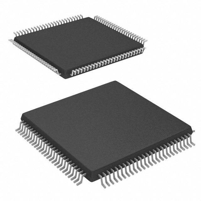
SPC56EL70L3, SPC56EL70L5,PC564L70L3, SPC564L70L5 Package pinouts and signal descrip- 2 Package pinouts and signal descriptions 2.1 Package pinouts Figure 2 shows the SPC56XL70 in the LQFP100 package. Figure 2. SPC56XL70 LQFP100 package A[15]A[14]C[6]FCCU_F[1]B[6]A[13]A[9]VSS_LV_CORVDD_LV_CORVDD_HV_REG_2D[4]D[3]VSS_HV_IOVDD_HV_IOD[0]C[15]JCOMPA[12]A[11]A[10]B[3]B[2]C[10]B[1]B[0] 100100999998989797969695959494939392929191909089898888878786868585848483838282818180807979787877777676 NMI 11 775 A[4] A[6] 2 74 VPP_TEST D[1] 3 573 D[14] A[7] 42 72 C[14] C[4] 5 7714 C[13] A[8] 6 7703 D[12] C[5] 73 6792 VDD_HV_FLA A[5] 8 6781 VSS_HV_FLA C[7] 9 6770 VDD_HV_REG_1 VDD_HV_REG_0 140 6669 VSS_LV_COR VSS_LV_COR 11 6658 VDD_LV_COR VDD_LV_COR 12 LLQQFFPP110000 ppaacckkaaggee 6647 A[3] VVDSDS__HHVV__IIOO 11534 66663265 VVDSSD__HHVV__IOIO D[9] 15 6614 B[4] VDD_HV_OSC 16 6603 TCK VSS_HV_OSC 167 5692 TMS XTAL 18 5681 B[5] EXTAL 19 5670 A[2] RESET 270 5569 C[12] D[8] 21 5558 C[11] D[5] 22 5547 D[11] D[6] 283 5536 D[10] VSS_LV_PLL0_PLL1 24 5525 A[1] VDD_LV_PLL0_PLL1 25 5514 A[0] 226272862930312323373435362373883940412424394445463474849050 D[7]FCCU_F[0]VDD_LV_CORVSS_LV_CORB[7]B[8]E[2]VDD_HV_ADR0VSS_HV_ADR0B[9]B[10]B[11]B[12]VDD_HV_ADR1VSS_HV_ADR1VDD_HV_ADVVSS_HV_ADVB[13]B[14]C[0]E[0]BCTRLVDD_LV_CORVSS_LV_CORVDD_HV_PMU DocID023953 Rev 5 33/128 127
Package pinouts and signal descriptions SPC56EL70L3, SPC56EL70L5,PC564L70L3, Figure 3 shows the SPC56XL70 in the LQFP144 package. Figure 3. SPC56XL70 LQFP144 pinout (top view) A[15]A[14]C[6]FCCU_F[1]D[2]F[3]B[6]VSS_LV_CORA[13]VDD_LV_CORA[9]F[0]VSS_LV_CORVDD_LV_CORVDD_HV_REG_2D[4]D[3]VSS_HV_IOVDD_HV_IOD[0]C[15]JCOMPA[12]E[15]A[11]E[14]A[10]E[13]B[3]F[14]B[2]F[15]F[13]C[10]B[1]B[0] NMI 1 144143142141140139138137136135134133132131130129128127126125124123122121120119118117116115114113112111110109108 A[4] A[6] 2 107 VPP_TEST D[1] 3 106 F[12] F[4] 4 105 D[14] F[5] 5 104 G[3] VDD_HV_IO 6 103 C[14] VSS_HV_IO 7 102 G[2] F[6] 8 101 C[13] MDO0 9 100 G[4] A[7] 10 99 D[12] C[4] 11 98 G[6] A[8] 12 97 VDD_HV_FLA C[5] 13 96 VSS_HV_FLA A[5] 14 95 VDD_HV_REG_1 C[7] 15 94 VSS_LV_COR VDD_HV_REG_0 16 93 VDD_LV_COR VSS_LV_COR 17 92 A[3] VDD_LV_COR 18 LQFP144 package 91 VDD_HV_IO F[7] 19 90 VSS_HV_IO F[8] 20 89 B[4] VDD_HV_IO 21 88 TCK VSS_HV_IO 22 87 TMS F[9] 23 86 B[5] F[10] 24 85 G[5] F[11] 25 84 A[2] D[9] 26 83 G[7] VDD_HV_OSC 27 82 C[12] VSS_HV_OSC 28 81 G[8] XTAL 29 80 C[11] EXTAL 30 79 G[9] RESET 31 78 D[11] D[8] 32 77 G[10] D[5] 33 76 D[10] D[6] 34 75 G[11] VSS_LV_PLL0_PLL1 35 74 A[1] VDD_LV_PLL0_PLL1 36 73 A[0] 373839404142434445464748495051525354555657585960616263646566676869707172 D[7]FCCU_F[0]VDD_LV_CORVSS_LV_CORC[1]E[4]B[7]E[5]C[2]E[6]B[8]E[7]E[2]VDD_HV_ADR0VSS_HV_ADR0B[9]B[10]B[11]B[12]VDD_HV_ADR1VSS_HV_ADR1VDD_HV_ADVVSS_HV_ADVB[13]E[9]B[15]E[10]B[14]E[11]C[0]E[12]E[0]BCTRLVDD_LV_CORVSS_LV_CORVDD_HV_PMU Table 3 and Table 4 provides the pin function summaries for the 100-pin and 144-pin packages respectively, listing all the signals multiplexed to each pin Table 3. LQFP100 pin function summary Pin # Port/function Peripheral Output function Input function 1 NMI — SIUL GPIO[6] GPIO[6] 2 A[6] DSPI_1 SCK SCK SIUL — EIRQ[6] SIUL GPIO[49] GPIO[49] eTimer_1 ETC[2] ETC[2] 3 D[1] CTU_0 EXT_TGR — FlexRay — CA_RX 34/128 DocID023953 Rev 5
SPC56EL70L3, SPC56EL70L5,PC564L70L3, SPC564L70L5 Package pinouts and signal descrip- Table 3. LQFP100 pin function summary (continued) Pin # Port/function Peripheral Output function Input function SIUL GPIO[7] GPIO[7] DSPI_1 SOUT — 4 A[7] SIUL — EIRQ[7] FlexCan_2 — RXD SIUL GPIO[36] GPIO[36] DSPI_0 CS0 CS0 5 C[4] FlexPWM_0 X[1] X[1] SSCM DEBUG[4] — SIUL — EIRQ[22] SIUL GPIO[8] GPIO[8] DSPI_1 — SIN 6 A[8] SIUL — EIRQ[8] FlexCan_2 TXD — SIUL GPIO[37] GPIO[37] DSPI_0 SCK SCK 7 C[5] SSCM DEBUG[5] — FlexPWM_0 — FAULT[3] SIUL — EIRQ[23] SIUL GPIO[5] GPIO[5] DSPI_1 CS0 CS0 8 A[5] eTimer_1 ETC[5] ETC[5] DSPI_0 CS7 — SIUL — EIRQ[5] SIUL GPIO[39] GPIO[39] FlexPWM_0 A[1] A[1] 9 C[7] SSCM DEBUG[7] — DSPI_0 — SIN 10 V — DD_HV_REG_0 11 V — SS_LV_COR 12 V — DD_LV_COR 13 V — DD_HV_IO 14 V — SS_HV_IO SIUL GPIO[57] GPIO[57] 15 D[9] FlexPWM_0 X[0] X[0] LINFlexD_1 TXD — DocID023953 Rev 5 35/128 127
Package pinouts and signal descriptions SPC56EL70L3, SPC56EL70L5,PC564L70L3, Table 3. LQFP100 pin function summary (continued) Pin # Port/function Peripheral Output function Input function 16 V — DD_HV_OSC 17 V — SS_HV_OSC 18 XTALIN — 19 XTALOUT — 20 RESET — SIUL GPIO[56] GPIO[56] DSPI_1 CS2 — 21 D[8] eTimer_1 ETC[4] ETC[4] DSPI_0 CS5 — FlexPWM_0 — FAULT[3] SIUL GPIO[53] GPIO[53] 22 D[5] DSPI_0 CS3 — FlexPWM_0 — FAULT[2] SIUL GPIO[54] GPIO[54] DSPI_0 CS2 — 23 D[6] FlexPWM_0 X[3] X[3] FlexPWM_0 — FAULT[1] 24 V — SS_LV_PLL0_PLL1 25 V — DD_LV_PLL0_PLL1 SIUL GPIO[55] GPIO[55] DSPI_1 CS3 — 26 D[7] DSPI_0 CS4 — SWG Analog output — 27 FCCU_F[0] FCCU F[0] F[0] 28 V — DD_LV_COR 29 V — SS_LV_COR SIUL — GPIO[23] 30 B[7] LINFlexD_0 — RXD ADC_0 — AN[0] SIUL — GPIO[24] 31 B[8] eTimer_0 — ETC[5] ADC_0 — AN[1] SIUL — GPIO[66] 32 E[2] ADC_0 — AN[5] 33 V — DD_HV_ADR0 36/128 DocID023953 Rev 5
SPC56EL70L3, SPC56EL70L5,PC564L70L3, SPC564L70L5 Package pinouts and signal descrip- Table 3. LQFP100 pin function summary (continued) Pin # Port/function Peripheral Output function Input function 34 V — SS_HV_ADR0 SIUL — GPIO[25] 35 B[9] ADC_0 — AN[11] ADC_1 SIUL — GPIO[26] 36 B[10] ADC_0 — AN[12] ADC_1 SIUL — GPIO[27] 37 B[11] ADC_0 — AN[13] ADC_1 SIUL — GPIO[28] 38 B[12] ADC_0 — AN[14] ADC_1 39 V — DD_HV_ADR1 40 V — SS_HV_ADR1 41 V — DD_HV_ADV 42 V — SS_HV_ADV SIUL — GPIO[29] 43 B[13] LINFlexD_1 — RXD ADC_1 — AN[0] SIUL — GPIO[30] eTimer_0 — ETC[4] 44 B[14] SIUL — EIRQ[19] ADC_1 — AN[1] SIUL — GPIO[32] 45 C[0] ADC_1 — AN[3] SIUL — GPIO[64] 46 E[0] ADC_1 — AN[5] 47 BCTRL — 48 V — DD_LV_COR 49 V — SS_LV_COR 50 V — DD_HV_PMU DocID023953 Rev 5 37/128 127
Package pinouts and signal descriptions SPC56EL70L3, SPC56EL70L5,PC564L70L3, Table 3. LQFP100 pin function summary (continued) Pin # Port/function Peripheral Output function Input function SIUL GPIO[0] GPIO[0] eTimer_0 ETC[0] ETC[0] 51 A[0] DSPI_2 SCK SCK SIUL — EIRQ[0] SIUL GPIO[1] GPIO[1] eTimer_0 ETC[1] ETC[1] 52 A[1] DSPI_2 SOUT — SIUL — EIRQ[1] SIUL GPIO[58] GPIO[58] 53 D[10] FlexPWM_0 A[0] A[0] eTimer_0 — ETC[0] SIUL GPIO[59] GPIO[59] 54 D[11] FlexPWM_0 B[0] B[0] eTimer_0 — ETC[1] SIUL GPIO[43] GPIO[43] 55 C[11] eTimer_0 ETC[4] ETC[4] DSPI_2 CS2 — SIUL GPIO[44] GPIO[44] 56 C[12] eTimer_0 ETC[5] ETC[5] DSPI_2 CS3 — SIUL GPIO[2] GPIO[2] eTimer_0 ETC[2] ETC[2] FlexPWM_0 A[3] A[3] 57 A[2] DSPI_2 — SIN MC_RGM — ABS[0] SIUL — EIRQ[2] SIUL GPIO[21] GPIO[21] 58 B[5] JTAGC — TDI 59 TMS — 60 TCK — SIUL GPIO[20] GPIO[20] 61 B[4] JTAGC TDO — 62 V — SS_HV_IO 63 V — DD_HV_IO 38/128 DocID023953 Rev 5
SPC56EL70L3, SPC56EL70L5,PC564L70L3, SPC564L70L5 Package pinouts and signal descrip- Table 3. LQFP100 pin function summary (continued) Pin # Port/function Peripheral Output function Input function SIUL GPIO[3] GPIO[3] eTimer_0 ETC[3] ETC[3] DSPI_2 CS0 CS0 64 A[3] FlexPWM_0 B[3] B[3] MC_RGM — ABS[2] SIUL — EIRQ[3] 65 V — DD_LV_COR 66 V — SS_LV_COR 67 V — DD_HV_REG_1 68 V — SS_HV_FLA 69 V — DD_HV_FLA SIUL GPIO[60] GPIO[60] 70 D[12] FlexPWM_0 X[1] X[1] LINFlexD_1 — RXD SIUL GPIO[45] GPIO[45] eTimer_1 ETC[1] ETC[1] 71 C[13] CTU_0 — EXT_IN FlexPWM_0 — EXT_SYNC SIUL GPIO[46] GPIO[46] 72 C[14] eTimer_1 ETC[2] ETC[2] CTU_0 EXT_TGR — SIUL GPIO[62] GPIO[62] 73 D[14] FlexPWM_0 B[1] B[1] eTimer_0 — ETC[3] 74 V (1) — PP_TEST SIUL GPIO[4] GPIO[4] eTimer_1 ETC[0] ETC[0] DSPI_2 CS1 — 75 A[4] eTimer_0 ETC[4] ETC[4] MC_RGM — FAB SIUL — EIRQ[4] DocID023953 Rev 5 39/128 127
Package pinouts and signal descriptions SPC56EL70L3, SPC56EL70L5,PC564L70L3, Table 3. LQFP100 pin function summary (continued) Pin # Port/function Peripheral Output function Input function SIUL GPIO[16] GPIO[16] FlexCAN_0 TXD — 76 B[0] eTimer_1 ETC[2] ETC[2] SSCM DEBUG[0] — SIUL — EIRQ[15] SIUL GPIO[17] GPIO[17] eTimer_1 ETC[3] ETC[3] SSCM DEBUG[1] — 77 B[1] FlexCAN_0 — RXD FlexCAN_1 — RXD SIUL — EIRQ[16] SIUL GPIO[42] GPIO[42] DSPI_2 CS2 — 78 C[10] FlexPWM_0 A[3] A[3] FlexPWM_0 — FAULT[1] SIUL GPIO[18] GPIO[18] LINFlexD_0 TXD — 79 B[2] SSCM DEBUG[2] DEBUG[2] SIUL — EIRQ[17] SIUL GPIO[19] GPIO[19] 80 B[3] SSCM DEBUG[3] DEBUG[3] LINFlexD_0 — RXD SIUL GPIO[10] GPIO[10] DSPI_2 CS0 CS0 81 A[10] FlexPWM_0 B[0] B[0] FlexPWM_0 X[2] X[2] SIUL — EIRQ[9] SIUL GPIO[11] GPIO[11] DSPI_2 SCK SCK 82 A[11] FlexPWM_0 A[0] A[0] FlexPWM_0 A[2] A[2] SIUL — EIRQ[10] 40/128 DocID023953 Rev 5
SPC56EL70L3, SPC56EL70L5,PC564L70L3, SPC564L70L5 Package pinouts and signal descrip- Table 3. LQFP100 pin function summary (continued) Pin # Port/function Peripheral Output function Input function SIUL GPIO[12] GPIO[12] DSPI_2 SOUT — 83 A[12] FlexPWM_0 A[2] A[2] FlexPWM_0 B[2] B[2] SIUL — EIRQ[11] 84 JCOMP — — JCOMP SIUL GPIO[47] GPIO[47] FlexRay CA_TR_EN — eTimer_1 ETC[0] ETC[0] 85 C[15] FlexPWM_0 A[1] A[1] CTU_0 — EXT_IN FlexPWM_0 — EXT_SYNC SIUL GPIO[48] GPIO[48] FlexRay CA_TX — 86 D[0] eTimer_1 ETC[1] ETC[1] FlexPWM_0 B[1] B[1] 87 V — DD_HV_IO 88 V — SS_HV_IO SIUL GPIO[51] GPIO[51] FlexRay CB_TX — 89 D[3] eTimer_1 ETC[4] ETC[4] FlexPWM_0 A[3] A[3] SIUL GPIO[52] GPIO[52] FlexRay CB_TR_EN — 90 D[4] eTimer_1 ETC[5] ETC[5] FlexPWM_0 B[3] B[3] 91 V — DD_HV_REG_2 92 V — DD_LV_COR 93 V — SS_LV_COR SIUL GPIO[9] GPIO[9] DSPI_2 CS1 — 94 A[9] FlexPWM_0 B[3] B[3] FlexPWM_0 — FAULT[0] DocID023953 Rev 5 41/128 127
Package pinouts and signal descriptions SPC56EL70L3, SPC56EL70L5,PC564L70L3, Table 3. LQFP100 pin function summary (continued) Pin # Port/function Peripheral Output function Input function SIUL GPIO[13] GPIO[13] FlexPWM_0 B[2] B[2] 95 A[13] DSPI_2 — SIN FlexPWM_0 — FAULT[0] SIUL — EIRQ[12] SIUL GPIO[22] GPIO[22] MC_CGM clk_out — 96 B[6] DSPI_2 CS2 — SIUL — EIRQ[18] 97 FCCU_F[1] FCCU F[1] F[1] SIUL GPIO[38] GPIO[38] DSPI_0 SOUT — 98 C[6] FlexPWM_0 B[1] B[1] SSCM DEBUG[6] — SIUL — EIRQ[24] SIUL GPIO[14] GPIO[14] FlexCAN_1 TXD — 99 A[14] eTimer_1 ETC[4] ETC[4] SIUL — EIRQ[13] SIUL GPIO[15] GPIO[15] eTimer_1 ETC[5] ETC[5] 100 A[15] FlexCAN_1 — RXD FlexCAN_0 — RXD SIUL — EIRQ[14] 1. V should always be tied to ground (V ) for normal operations. PP_TEST SS Table 4. LQFP144 pin function summary Pin # Port/function Peripheral Output function Input function 1 NMI — SIUL GPIO[6] GPIO[6] 2 A[6] DSPI_1 SCK SCK SIUL — EIRQ[6] 42/128 DocID023953 Rev 5
SPC56EL70L3, SPC56EL70L5,PC564L70L3, SPC564L70L5 Package pinouts and signal descrip- Table 4. LQFP144 pin function summary (continued) Pin # Port/function Peripheral Output function Input function SIUL GPIO[49] GPIO[49] eTimer_1 ETC[2] ETC[2] 3 D[1] CTU_0 EXT_TGR — FlexRay — CA_RX SIUL GPIO[84] GPIO[84] 4 F[4] NPC MDO[3] — SIUL GPIO[85] GPIO[85] 5 F[5] NPC MDO[2] — 6 V — DD_HV_IO 7 V — SS_HV_IO SIUL GPIO[86] GPIO[86] 8 F[6] NPC MDO[1] — 9 MDO0 — SIUL GPIO[7] GPIO[7] DSPI_1 SOUT — 10 A[7] SIUL — EIRQ[7] FlexCAN_2 — RXD SIUL GPIO[36] GPIO[36] DSPI_0 CS0 CS0 11 C[4] FlexPWM_0 X[1] X[1] SSCM DEBUG[4] — SIUL — EIRQ[22] SIUL GPIO[8] GPIO[8] DSPI_1 — SIN 12 A[8] SIUL — EIRQ[8] FlexCAN_2 TXD — SIUL GPIO[37] GPIO[37] DSPI_0 SCK SCK 13 C[5] SSCM DEBUG[5] — FlexPWM_0 — FAULT[3] SIUL — EIRQ[23] DocID023953 Rev 5 43/128 127
Package pinouts and signal descriptions SPC56EL70L3, SPC56EL70L5,PC564L70L3, Table 4. LQFP144 pin function summary (continued) Pin # Port/function Peripheral Output function Input function SIUL GPIO[5] GPIO[5] DSPI_1 CS0 CS0 14 A[5] eTimer_1 ETC[5] ETC[5] DSPI_0 CS7 — SIUL — EIRQ[5] SIUL GPIO[39] GPIO[39] FlexPWM_0 A[1] A[1] 15 C[7] SSCM DEBUG[7] — DSPI_0 — SIN 16 V — DD_HV_REG_0 17 V — SS_LV_COR 18 V — DD_LV_COR SIUL GPIO[87] GPIO[87] 19 F[7] NPC MCKO — SIUL GPIO[88] GPIO[88] 20 F[8] NPC MSEO[1] — 21 V — DD_HV_IO 22 V — SS_HV_IO SIUL GPIO[89] GPIO[89] 23 F[9] NPC MSEO[0] — SIUL GPIO[90] GPIO[90] 24 F[10] NPC EVTO — SIUL GPIO[91] GPIO[91] 25 F[11] NPC EVTI — SIUL GPIO[57] GPIO[57] 26 D[9] FlexPWM_0 X[0] X[0] LINFlexD_1 TXD — 27 V — DD_HV_OSC 28 V — SS_HV_OSC 29 XTALIN — 30 XTALOUT — 31 RESET — 44/128 DocID023953 Rev 5
SPC56EL70L3, SPC56EL70L5,PC564L70L3, SPC564L70L5 Package pinouts and signal descrip- Table 4. LQFP144 pin function summary (continued) Pin # Port/function Peripheral Output function Input function SIUL GPIO[56] GPIO[56] DSPI_1 CS2 — 32 D[8] eTimer_1 ETC[4] ETC[4] DSPI_0 CS5 — FlexPWM_0 — FAULT[3] SIUL GPIO[53] GPIO[53] 33 D[5] DSPI_0 CS3 — FlexPWM_0 — FAULT[2] SIUL GPIO[54] GPIO[54] DSPI_0 CS2 — 34 D[6] FlexPWM_0 X[3] X[3] FlexPWM_0 — FAULT[1] 35 V — SS_LV_PLL0_PLL1 36 V — DD_LV_PLL0_PLL1 SIUL GPIO[55] GPIO[55] DSPI_1 CS3 — 37 D[7] DSPI_0 CS4 — SWG analog output — 38 FCCU_F[0] FCCU F[0] F[0] 39 V — DD_LV_COR 40 V — SS_LV_COR SIUL — GPIO[33] 41 C[1] ADC_0 — AN[2] SIUL — GPIO[68] 42 E[4] ADC_0 — AN[7] SIUL — GPIO[23] 43 B[7] LINFlexD_0 — RXD ADC_0 — AN[0] SIUL — GPIO[69] 44 E[5] ADC_0 — AN[8] SIUL — GPIO[34] 45 C[2] ADC_0 — AN[3] SIUL — GPIO[70] 46 E[6] ADC_0 — AN[4] DocID023953 Rev 5 45/128 127
Package pinouts and signal descriptions SPC56EL70L3, SPC56EL70L5,PC564L70L3, Table 4. LQFP144 pin function summary (continued) Pin # Port/function Peripheral Output function Input function SIUL — GPIO[24] 47 B[8] eTimer_0 — ETC[5] ADC_0 — AN[1] SIUL — GPIO[71] 48 E[7] ADC_0 — AN[6] SIUL — GPIO[66] 49 E[2] ADC_0 — AN[5] 50 V — DD_HV_ADR0 51 V — SS_HV_ADR0 SIUL — GPIO[25] 52 B[9] ADC_0 — AN[11] ADC_1 SIUL — GPIO[26] 53 B[10] ADC_0 — AN[12] ADC_1 SIUL — GPIO[27] 54 B[11] ADC_0 — AN[13] ADC_1 SIUL — GPIO[28] 55 B[12] ADC_0 — AN[14] ADC_1 56 V — DD_HV_ADR1 57 V — SS_HV_ADR1 58 V — DD_HV_ADV 59 V — SS_HV_ADV SIUL — GPIO[29] 60 B[13] LINFlexD_1 — RXD ADC_1 — AN[0] SIUL — GPIO[73] 61 E[9] ADC_1 — AN[7] SIUL — GPIO[31] 62 B[15] SIUL — EIRQ[20] ADC_1 — AN[2] SIUL — GPIO[74] 63 E[10] ADC_1 — AN[8] 46/128 DocID023953 Rev 5
SPC56EL70L3, SPC56EL70L5,PC564L70L3, SPC564L70L5 Package pinouts and signal descrip- Table 4. LQFP144 pin function summary (continued) Pin # Port/function Peripheral Output function Input function SIUL — GPIO[30] eTimer_0 — ETC[4] 64 B[14] SIUL — EIRQ[19] ADC_1 — AN[1] SIUL — GPIO[75] 65 E[11] ADC_1 — AN[4] SIUL — GPIO[32] 66 C[0] ADC_1 — AN[3] SIUL — GPIO[76] 67 E[12] ADC_1 — AN[6] SIUL — GPIO[64] 68 E[0] ADC_1 — AN[5] 69 BCTRL — 70 V — DD_LV_COR 71 V — SS_LV_COR 72 V — DD_HV_PMU SIUL GPIO[0] GPIO[0] eTimer_0 ETC[0] ETC[0] 73 A[0] DSPI_2 SCK SCK SIUL — EIRQ[0] SIUL GPIO[1] GPIO[1] eTimer_0 ETC[1] ETC[1] 74 A[1] DSPI_2 SOUT — SIUL — EIRQ[1] SIUL GPIO[107] GPIO[107] 75 G[11] FlexRay DBG3 — FlexPWM_0 — FAULT[3] SIUL GPIO[58] GPIO[58] 76 D[10] FlexPWM_0 A[0] A[0] eTimer_0 — ETC[0] SIUL GPIO[106] GPIO[106] FlexRay DBG2 — 77 G[10] DSPI_2 CS3 — FlexPWM_0 — FAULT[2] DocID023953 Rev 5 47/128 127
Package pinouts and signal descriptions SPC56EL70L3, SPC56EL70L5,PC564L70L3, Table 4. LQFP144 pin function summary (continued) Pin # Port/function Peripheral Output function Input function SIUL GPIO[59] GPIO[59] 78 D[11] FlexPWM_0 B[0] B[0] eTimer_0 — ETC[1] SIUL GPIO[105] GPIO[105] FlexRay DBG1 — 79 G[9] DSPI_1 CS1 — FlexPWM_0 — FAULT[1] SIUL — EIRQ[29] SIUL GPIO[43] GPIO[43] 80 C[11] eTimer_0 ETC[4] ETC[4] DSPI_2 CS2 — SIUL GPIO[104] GPIO[104] FlexRay DBG0 — 81 G[8] DSPI_0 CS1 — FlexPWM_0 — FAULT[0] SIUL — EIRQ[21] SIUL GPIO[44] GPIO[44] 82 C[12] eTimer_0 ETC[5] ETC[5] DSPI_2 CS3 — SIUL GPIO[103] GPIO[103] 83 G[7] FlexPWM_0 B[3] B[3] SIUL GPIO[2] GPIO[2] eTimer_0 ETC[2] ETC[2] FlexPWM_0 A[3] A[3] 84 A[2] DSPI_2 — SIN MC_RGM — ABS[0] SIUL — EIRQ[2] SIUL GPIO[101] GPIO[101] 85 G[5] FlexPWM_0 X[3] X[3] DSPI_2 CS3 — SIUL GPIO[21] GPIO[21] 86 B[5] JTAGC — TDI 87 TMS — 88 TCK — 48/128 DocID023953 Rev 5
SPC56EL70L3, SPC56EL70L5,PC564L70L3, SPC564L70L5 Package pinouts and signal descrip- Table 4. LQFP144 pin function summary (continued) Pin # Port/function Peripheral Output function Input function SIUL GPIO[20] GPIO[20] 89 B[4] JTAGC TDO — 90 V — SS_HV_IO 91 V — DD_HV_IO SIUL GPIO[3] GPIO[3] eTimer_0 ETC[3] ETC[3] DSPI_2 CS0 CS0 92 A[3] FlexPWM_0 B[3] B[3] MC_RGM — ABS[2] SIUL — EIRQ[3] 93 V — DD_LV_COR 94 V — SS_LV_COR 95 V — DD_HV_REG_1 96 V — SS_HV_FLA 97 V — DD_HV_FLA SIUL GPIO[102] GPIO[102] 98 G[6] FlexPWM_0 A[3] A[3] SIUL GPIO[60] GPIO[60] 99 D[12] FlexPWM_0 X[1] X[1] LINFlexD_1 — RXD SIUL GPIO[100] GPIO[100] 100 G[4] FlexPWM_0 B[2] B[2] eTimer_0 — ETC[5] SIUL GPIO[45] GPIO[45] eTimer_1 ETC[1] ETC[1] 101 C[13] CTU_0 — EXT_IN FlexPWM_0 — EXT_SYNC SIUL GPIO[98] GPIO[98] 102 G[2] FlexPWM_0 X[2] X[2] DSPI_1 CS1 — SIUL GPIO[46] GPIO[46] 103 C[14] eTimer_1 ETC[2] ETC[2] CTU_0 EXT_TGR — DocID023953 Rev 5 49/128 127
Package pinouts and signal descriptions SPC56EL70L3, SPC56EL70L5,PC564L70L3, Table 4. LQFP144 pin function summary (continued) Pin # Port/function Peripheral Output function Input function SIUL GPIO[99] GPIO[99] 104 G[3] FlexPWM_0 A[2] A[2] eTimer_0 — ETC[4] SIUL GPIO[62] GPIO[62] 105 D[14] FlexPWM_0 B[1] B[1] eTimer_0 — ETC[3] SIUL GPIO[92] GPIO[92] 106 F[12] eTimer_1 ETC[3] ETC[3] SIUL — EIRQ[30] 107 V (1) — PP_TEST SIUL GPIO[4] GPIO[4] eTimer_1 ETC[0] ETC[0] DSPI_2 CS1 — 108 A[4] eTimer_0 ETC[4] ETC[4] MC_RGM — FAB SIUL — EIRQ[4] SIUL GPIO[16] GPIO[16] FlexCAN_0 TXD — 109 B[0] eTimer_1 ETC[2] ETC[2] SSCM DEBUG[0] — SIUL — EIRQ[15] SIUL GPIO[17] GPIO[17] eTimer_1 ETC[3] ETC[3] SSCM DEBUG[1] — 110 B[1] FlexCAN_0 — RXD FlexCAN_1 — RXD SIUL — EIRQ[16] SIUL GPIO[42] GPIO[42] DSPI_2 CS2 — 111 C[10] FlexPWM_0 A[3] A[3] FlexPWM_0 — FAULT[1] SIUL GPIO[93] GPIO[93] 112 F[13] eTimer_1 ETC[4] ETC[4] SIUL — EIRQ[31] 50/128 DocID023953 Rev 5
SPC56EL70L3, SPC56EL70L5,PC564L70L3, SPC564L70L5 Package pinouts and signal descrip- Table 4. LQFP144 pin function summary (continued) Pin # Port/function Peripheral Output function Input function SIUL GPIO[95] GPIO[95] 113 F[15] LINFlexD_1 — RXD FlexCAN_2 TXD — SIUL GPIO[18] GPIO[18] LINFlexD_0 TXD — 114 B[2] SSCM DEBUG[2] — SIUL — EIRQ[17] SIUL GPIO[94] GPIO[94] 115 F[14] LINFlexD_1 TXD — FlexCAN_2 — RXD SIUL GPIO[19] GPIO[19] 116 B[3] SSCM DEBUG[3] — LINFlexD_0 — RXD SIUL GPIO[77] GPIO[77] eTimer_0 ETC[5] ETC[5] 117 E[13] DSPI_2 CS3 — SIUL — EIRQ[25] SIUL GPIO[10] GPIO[10] DSPI_2 CS0 CS0 118 A[10] FlexPWM_0 B[0] B[0] FlexPWM_0 X[2] X[2] SIUL — EIRQ[9] SIUL GPIO[78] GPIO[78] 119 E[14] eTimer_1 ETC[5] ETC[5] SIUL — EIRQ[26] SIUL GPIO[11] GPIO[11] DSPI_2 SCK SCK 120 A[11] FlexPWM_0 A[0] A[0] FlexPWM_0 A[2] A[2] SIUL — EIRQ[10] SIUL GPIO[79] GPIO[79] 121 E[15] DSPI_0 CS1 — SIUL — EIRQ[27] DocID023953 Rev 5 51/128 127
Package pinouts and signal descriptions SPC56EL70L3, SPC56EL70L5,PC564L70L3, Table 4. LQFP144 pin function summary (continued) Pin # Port/function Peripheral Output function Input function SIUL GPIO[12] GPIO[12] DSPI_2 SOUT — 122 A[12] FlexPWM_0 A[2] A[2] FlexPWM_0 B[2] B[2] SIUL — EIRQ[11] 123 JCOMP — — JCOMP SIUL GPIO[47] GPIO[47] FlexRay CA_TR_EN — eTimer_1 ETC[0] ETC[0] 124 C[15] FlexPWM_0 A[1] A[1] CTU_0 — EXT_IN FlexPWM_0 — EXT_SYNC SIUL GPIO[48] GPIO[48] FlexRay CA_TX — 125 D[0] eTimer_1 ETC[1] ETC[1] FlexPWM_0 B[1] B[1] 126 V — DD_HV_IO 127 V — SS_HV_IO SIUL GPIO[51] GPIO[51] FlexRay CB_TX — 128 D[3] eTimer_1 ETC[4] ETC[4] FlexPWM_0 A[3] A[3] SIUL GPIO[52] GPIO[52] FlexRay CB_TR_EN — 129 D[4] eTimer_1 ETC[5] ETC[5] FlexPWM_0 B[3] B[3] 130 V — DD_HV_REG_2 131 V — DD_LV_COR 132 V — SS_LV_COR SIUL GPIO[80] GPIO[80] FlexPWM_0 A[1] A[1] 133 F[0] eTimer_0 — ETC[2] SIUL — EIRQ[28] 52/128 DocID023953 Rev 5
SPC56EL70L3, SPC56EL70L5,PC564L70L3, SPC564L70L5 Package pinouts and signal descrip- Table 4. LQFP144 pin function summary (continued) Pin # Port/function Peripheral Output function Input function SIUL GPIO[9] GPIO[9] DSPI_2 CS1 — 134 A[9] FlexPWM_0 B[3] B[3] FlexPWM_0 — FAULT[0] 135 V — DD_LV_COR SIUL GPIO[13] GPIO[13] FlexPWM_0 B[2] B[2] 136 A[13] DSPI_2 — SIN FlexPWM_0 — FAULT[0] SIUL — EIRQ[12] 137 V — SS_LV_COR SIUL GPIO[22] GPIO[22] MC_CGM clk_out — 138 B[6] DSPI_2 CS2 — SIUL — EIRQ[18] SIUL GPIO[83] GPIO[83] 139 F[3] DSPI_0 CS6 — SIUL GPIO[50] GPIO[50] eTimer_1 ETC[3] ETC[3] 140 D[2] FlexPWM_0 X[3] X[3] FlexRay — CB_RX 141 FCCU_F[1] FCCU F[1] F[1] SIUL GPIO[38] GPIO[38] DSPI_0 SOUT — 142 C[6] FlexPWM_0 B[1] B[1] SSCM DEBUG[6] — SIUL — EIRQ[24] SIUL GPIO[14] GPIO[14] FlexCAN_1 TXD — 143 A[14] eTimer_1 ETC[4] ETC[4] SIUL — EIRQ[13] DocID023953 Rev 5 53/128 127
Package pinouts and signal descriptions SPC56EL70L3, SPC56EL70L5,PC564L70L3, Table 4. LQFP144 pin function summary (continued) Pin # Port/function Peripheral Output function Input function SIUL GPIO[15] GPIO[15] eTimer_1 ETC[5] ETC[5] 144 A[15] FlexCAN_1 — RXD FlexCAN_0 — RXD SIUL — EIRQ[14] 1. V should always be tied to ground (V ) for normal operations. PP_TEST SS 2.2 Supply pins Table 5. Supply pins Supply Pin # 100 144 Symbol Description Pkg Pkg VREG control and power supply pins BCTRL Voltage regulator external NPN ballast base control pin 47 69 V Core logic supply 48 70 DD_LV_COR V Core regulator ground 49 71 SS_LV_COR V Voltage regulator supply 50 72 DD_HV_PMU ADC_0/ADC_1 reference voltage and ADC supply V ADC_0 high reference voltage 33 50 DD_HV_ADR0 V ADC_0 low reference voltage 34 51 SS_HV_ADR0 V ADC_1 high reference voltage 39 56 DD_HV_ADR1 V ADC_1 low reference voltage 40 57 SS_HV_ADR1 V ADC voltage supply for ADC_0 and ADC_1 41 58 DD_HV_ADV V ADC ground for ADC_0 and ADC_1 42 59 SS_HV_ADV Power supply pins (3.3 V) V 3.3 V Input/Output supply voltage — 6 DD_HV_IO V 3.3 V Input/Output ground — 7 SS_HV_IO V VDD_HV_REG_0 10 16 DD_HV_REG_0 V 3.3 V Input/Output supply voltage 13 21 DD_HV_IO V 3.3 V Input/Output ground 14 22 SS_HV_IO V Crystal oscillator amplifier supply voltage 16 27 DD_HV_OSC V Crystal oscillator amplifier ground 17 28 SS_HV_OSC V 3.3 V Input/Output ground 62 90 SS_HV_IO V 3.3 V Input/Output supply voltage 63 91 DD_HV_IO 54/128 DocID023953 Rev 5
SPC56EL70L3, SPC56EL70L5,PC564L70L3, SPC564L70L5 Package pinouts and signal descrip- Table 5. Supply pins (continued) Supply Pin # 100 144 Symbol Description Pkg Pkg V VDD_HV_REG_1 67 95 DD_HV_REG_1 V VSS_HV_FLA 68 96 SS_HV_FLA V VDD_HV_FLA 69 97 DD_HV_FLA V VDD_HV_IO 87 126 DD_HV_IO V VSS_HV_IO 88 127 SS_HV_IO V VDD_HV_REG_2 91 130 DD_HV_REG_2 Power supply pins (1.2 V) VSS_LV_COR V Decoupling pins for core logic. Decoupling capacitor must be connected 11 17 SS_LV_COR between these pins and the nearest V pin. DD_LV_COR VDD_LV_COR V Decoupling pins for core logic. Decoupling capacitor must be connected 12 18 DD_LV_COR between these pins and the nearest V pin. SS_LV_COR VSS_LV_PLL0_PLL1 / V 1V2 1.2 V Decoupling pins for on-chip FMPLL modules. Decoupling capacitor must 24 35 SS be connected between this pin and V DD_LV_PLL. VDD_LV_PLL0_PLL1 V 1V2 Decoupling pins for on-chip FMPLL modules. Decoupling capacitor must be 25 36 DD connected between this pin and V SS_LV_PLL. VDD_LV_COR V Decoupling pins for core logic. Decoupling capacitor must be connected 28 39 DD_LV_COR between these pins and the nearest V pin. SS_LV_COR VSS_LV_COR V Decoupling pins for core logic. Decoupling capacitor must be connected 29 40 SS_LV_COR between these pins and the nearest V pin. DD_LV_COR VDD_LV_COR V Decoupling pins for core logic and Regulator feedback. Decoupling capacitor — 70 DD_LV_COR must be connected between this pins and V SS_LV_REGCOR. VSS_LV_REGCOR0 V Decoupling pins for core logic and Regulator feedback. Decoupling capacitor — 71 SS_LV_COR must be connected between this pins and V DD_LV_REGCOR. VDD_LV_COR V Decoupling pins for core logic. Decoupling capacitor must be connected 65 93 DD_LV_COR between these pins and the nearest V pin. SS_LV_COR VSS_LV_COR V / 1.2 V Decoupling pins for core logic. Decoupling capacitor must be connected 66 94 SS_LV_COR between these pins and the nearest V DD_LV_COR pin. VDD_LV_COR V 1V2 Decoupling pins for core logic. Decoupling capacitor must be connected 92 131 DD between these pins and the nearest V pin. DD_LV_COR DocID023953 Rev 5 55/128 127
Package pinouts and signal descriptions SPC56EL70L3, SPC56EL70L5,PC564L70L3, Table 5. Supply pins (continued) Supply Pin # 100 144 Symbol Description Pkg Pkg VSS_LV_COR V 1V2 Decoupling pins for core logic. Decoupling capacitor must be connected 93 132 SS between these pins and the nearest V pin. DD_LV_COR VDD_LV_COR / V 1V2 Decoupling pins for core logic. Decoupling capacitor must be connected — 135 DD between these pins and the nearest V pin. DD_LV_COR VSS_LV_COR / V 1V2 Decoupling pins for core logic. Decoupling capacitor must be connected — 137 SS between these pins and the nearest V pin. DD_LV_COR 2.3 System pins Table 6. System pins Pin # Symbol Description Direction 100 144 pkg pkg Dedicated pins MDO0(1) Nexus Message Data Output — line Output only — 9 NMI(2) Non Maskable Interrupt Input only 1 1 XTAL Input for oscillator amplifier circuit and internal clock generator Input only 18 29 EXTAL(3) Oscillator amplifier output Input/Output(4) 19 30 TMS(2) JTAG state machine control Input only 59 87 TCK(2) JTAG clock Input only 60 88 JCOMP(5) JTAG compliance select Input only 84 123 Reset pin RESET Bidirectional reset with Schmitt-Trigger characteristics and noise Bidirectional 20 31 filter. This pin has medium drive strength. Output drive is open drain and must be terminated by an external resistor of value 1KOhm.(6) Test pin VPP TEST Pin for testing purpose only. To be tied to ground in normal operating 74 107 mode. 1. This pad is configured for Fast (F) pad speed. 2. This pad contains a weak pull-up. 3. EXTAL is an "Output" in "crystal" mode, and is an "Input" in "ext clock" mode. 4. In XOSC Bypass Mode, the analog portion of crystal oscillator (amplifier) is disabled. An external clock can be applied at EXTAL as an input. In XOSC Normal Mode, EXTAL is an output 5. This pad contains a weak pull-down. 56/128 DocID023953 Rev 5
SPC56EL70L3, SPC56EL70L5,PC564L70L3, SPC564L70L5 Package pinouts and signal descrip- 6. RESET output shall be considered valid only after the 3.3V supply reaches its stable value. None of system pins (except RESET) provides an open drain output. 2.4 Pin muxing Table 7 defines the pin list and muxing for this device. Each entry of Table 7 shows all the possible configurations for each pin, via the alternate functions. The default function assigned to each pin after reset is indicated by ALT0. Note: Pins labeled “NC” are to be left unconnected. Any connection to an external circuit or voltage may cause unpredictable device behavior or damage. Pins labeled “Reserved” are to be tied to ground. Not doing so may cause unpredictable device behavior. Table 7. Pin muxing Weak Pad Pin # Alternate pull speed(1) Port Output Input Input mux PCR Peripheral output config name mux sel functions select function during SRC SRC 100 144 reset = 1 = 0 pkg pkg Port A SIUL GPIO[0] ALT0 GPIO[0] — PSMI[35]; eTimer_0 ETC[0] ALT1 ETC[0] PADSEL=0 Pull A[0] PCR[0] M S 51 73 down PSMI[1]; DSPI_2 SCK ALT2 SCK PADSEL=0 SIUL — — EIRQ[0] — SIUL GPIO[1] ALT0 GPIO[1] — PSMI[36]; eTimer_0 ETC[1] ALT1 ETC[1] A[1] PCR[1] PADSEL=0 Pull M S 52 74 down DSPI_2 SOUT ALT2 — — SIUL — — EIRQ[1] — SIUL GPIO[2] ALT0 GPIO[2] — PSMI[37]; eTimer_0 ETC[2] ALT1 ETC[2] PADSEL=0 PSMI[23]; A[2] PCR[2] FlexPWM_0 A[3] ALT3 A[3] PADSEL=0 Pull M S 57 84 down PSMI[2]; DSPI_2 — — SIN PADSEL=0 MC_RGM — — ABS[0] — SIUL — — EIRQ[2] — DocID023953 Rev 5 57/128 127
Package pinouts and signal descriptions SPC56EL70L3, SPC56EL70L5,PC564L70L3, Table 7. Pin muxing (continued) Weak Pad Pin # Alternate pull speed(1) Port Output Input Input mux PCR Peripheral output config name mux sel functions select function during SRC SRC 100 144 reset = 1 = 0 pkg pkg SIUL GPIO[3] ALT0 GPIO[3] — PSMI[38]; eTimer_0 ETC[3] ALT1 ETC[3] PADSEL=0 PSMI[3]; A[3] PCR[3] DSPI_2 CS0 ALT2 CS0 PADSEL=0 Pull M S 64 92 down PSMI[27]; FlexPWM_0 B[3] ALT3 B[3] PADSEL=0 MC_RGM — — ABS[2] — SIUL — — EIRQ[3] — SIUL GPIO[4] ALT0 GPIO[4] — PSMI[9]; eTimer_1 ETC[0] ALT1 ETC[0] PADSEL=0 DSPI_2 CS1 ALT2 — — Pull A[4] PCR[4] M S 75 108 PSMI[7]; down eTimer_0 ETC[4] ALT3 ETC[4] PADSEL=0 MC_RGM — — FAB — SIUL — — EIRQ[4] — SIUL GPIO[5] ALT0 GPIO[5] — DSPI_1 CS0 ALT1 CS0 — PSMI[14]; Pull A[5] PCR[5] eTimer_1 ETC[5] ALT2 ETC[5] M S 8 14 PADSEL=0 down DSPI_0 CS7 ALT3 — — SIUL — — EIRQ[5] — SIUL GPIO[6] ALT0 GPIO[6] — Pull A[6] PCR[6] DSPI_1 SCK ALT1 SCK — M S 2 2 down SIUL — — EIRQ[6] — SIUL GPIO[7] ALT0 GPIO[7] — DSPI_1 SOUT ALT1 — — Pull A[7] PCR[7] M S 4 10 SIUL — — EIRQ[7] — down FlexCAN_2 RXD ALT2 — — SIUL GPIO[8] ALT0 GPIO[8] — DSPI_1 — — SIN — Pull A[8] PCR[8] M S 6 12 SIUL — — EIRQ[8] — down FlexCAN_2 TXD ALT2 — — 58/128 DocID023953 Rev 5
SPC56EL70L3, SPC56EL70L5,PC564L70L3, SPC564L70L5 Package pinouts and signal descrip- Table 7. Pin muxing (continued) Weak Pad Pin # Alternate pull speed(1) Port Output Input Input mux PCR Peripheral output config name mux sel functions select function during SRC SRC 100 144 reset = 1 = 0 pkg pkg SIUL GPIO[9] ALT0 GPIO[9] — DSPI_2 CS1 ALT1 — — A[9] PCR[9] FlexPWM_0 B[3] ALT3 B[3] PPASDMSIE[2L7=];1 dPouwlln M S 94 134 PSMI[16]; FlexPWM_0 — — FAULT[0] PADSEL=0 SIUL GPIO[10] ALT0 GPIO[10] — PSMI[3]; DSPI_2 CS0 ALT1 CS0 PADSEL=1 PSMI[24]; Pull A[10] PCR[10] FlexPWM_0 B[0] ALT2 B[0] M S 81 118 PADSEL=0 down PSMI[29]; FlexPWM_0 X[2] ALT3 X[2] PADSEL=0 SIUL — — EIRQ[9] — SIUL GPIO[11] ALT0 GPIO[11] — PSMI[1]; DSPI_2 SCK ALT1 SCK PADSEL=1 PSMI[20]; Pull A[11] PCR[11] FlexPWM_0 A[0] ALT2 A[0] M S 82 120 PADSEL=0 down PSMI[22]; FlexPWM_0 A[2] ALT3 A[2] PADSEL=0 SIUL — — EIRQ[10] — SIUL GPIO[12] ALT0 GPIO[12] — DSPI_2 SOUT ALT1 — — PSMI[22]; FlexPWM_0 A[2] ALT2 A[2] Pull A[12] PCR[12] PADSEL=1 M S 83 122 down PSMI[26]; FlexPWM_0 B[2] ALT3 B[2] PADSEL=0 SIUL — — EIRQ[11] — DocID023953 Rev 5 59/128 127
Package pinouts and signal descriptions SPC56EL70L3, SPC56EL70L5,PC564L70L3, Table 7. Pin muxing (continued) Weak Pad Pin # Alternate pull speed(1) Port Output Input Input mux PCR Peripheral output config name mux sel functions select function during SRC SRC 100 144 reset = 1 = 0 pkg pkg SIUL GPIO[13] ALT0 GPIO[13] — PSMI[26]; FlexPWM_0 B[2] ALT2 B[2] PADSEL=1 PSMI[2]; Pull A[13] PCR[13] DSPI_2 — — SIN M S 95 136 PADSEL=1 down PSMI[16]; FlexPWM_0 — — FAULT[0] PADSEL=1 SIUL — — EIRQ[12] — SIUL GPIO[14] ALT0 GPIO[14] — FlexCAN_1 TXD ALT1 — — Pull A[14] PCR[14] eTimer_1 ETC[4] ALT2 ETC[4] PSMI[13]; down M S 99 143 PADSEL=0 SIUL — — EIRQ[13] — SIUL GPIO[15] ALT0 GPIO[15] — PSMI[14]; eTimer_1 ETC[5] ALT2 ETC[5] PADSEL=1 PSMI[34]; Pull A[15] PCR[15] FlexCAN_1 — — RXD M S 100 144 PADSEL=0 down PSMI[33]; FlexCAN_0 — — RXD PADSEL=0 SIUL — — EIRQ[14] — Port B SIUL GPIO[16] ALT0 GPIO[16] — FlexCAN_0 TXD ALT1 — — PSMI[11]; Pull B[0] PCR[16] eTimer_1 ETC[2] ALT2 ETC[2] M S 76 109 PADSEL=0 down SSCM DEBUG[0] ALT3 — — SIUL — — EIRQ[15] — 60/128 DocID023953 Rev 5
SPC56EL70L3, SPC56EL70L5,PC564L70L3, SPC564L70L5 Package pinouts and signal descrip- Table 7. Pin muxing (continued) Weak Pad Pin # Alternate pull speed(1) Port Output Input Input mux PCR Peripheral output config name mux sel functions select function during SRC SRC 100 144 reset = 1 = 0 pkg pkg SIUL GPIO[17] ALT0 GPIO[17] — PSMI[12]; eTimer_1 ETC[3] ALT2 ETC[3] PADSEL=0 SSCM DEBUG[1] ALT3 — — Pull B[1] PCR[17] M S 77 110 PSMI[33]; down FlexCAN_0 — — RXD PADSEL=1 PSMI[34]; FlexCAN_1 — — RXD PADSEL=1 SIUL — — EIRQ[16] — SIUL GPIO[18] ALT0 GPIO[18] — LINFlex_0 TXD ALT1 — — Pull B[2] PCR[18] M S 79 114 down SSCM DEBUG[2] ALT3 — — SIUL — — EIRQ[17] — SIUL GPIO[19] ALT0 GPIO[19] — SSCM DEBUG[3] ALT3 — — Pull B[3] PCR[19] M S 80 116 down PSMI[31]; LINFlex_0 — — RXD PADSEL=0 SIUL GPIO[20] ALT0 GPIO[20] — Pull B[4](2) PCR[20] F S 61 89 JTAGC TDO ALT1 — — down SIUL GPIO[21] ALT0 GPIO[21] — B[5] PCR[21] Pull up M S 58 86 JTAGC — — TDI — SIUL GPIO[22] ALT0 GPIO[22] — MC_CGM clk_out ALT1 — — Pull B[6] PCR[22] F S 96 138 down DSPI_2 CS2 ALT2 — — SIUL — EIRQ[18] — SIUL — ALT0 GPI[23] — PSMI[31]; B[7] PCR[23] LINFlex_0 — — RXD — — — 30 43 PADSEL=1 ADC_0 — — AN[0](3) — SIUL — ALT0 GPI[24] — PSMI[8]; B[8] PCR[24] eTimer_0 — — ETC[5] — — — 31 47 PADSEL=2 ADC_0 — — AN[1](3) — DocID023953 Rev 5 61/128 127
Package pinouts and signal descriptions SPC56EL70L3, SPC56EL70L5,PC564L70L3, Table 7. Pin muxing (continued) Weak Pad Pin # Alternate pull speed(1) Port Output Input Input mux PCR Peripheral output config name mux sel functions select function during SRC SRC 100 144 reset = 1 = 0 pkg pkg SIUL — ALT0 GPI[25] — B[9] PCR[25] ADC_0 — — — 35 52 — — AN[11](3) — ADC_1 SIUL — ALT0 GPI[26] — B[10] PCR[26] ADC_0 — — — 36 53 — — AN[12](3) — ADC_1 SIUL — ALT0 GPI[27] — B[11] PCR[27] ADC_0 — — — 37 54 — — AN[13](3) — ADC_1 SIUL — ALT0 GPI[28] — B[12] PCR[28] ADC_0 — — — 38 55 — — AN[14](3) — ADC_1 SIUL — ALT0 GPI[29] — PSMI[32]; B[13] PCR[29] LINFlex_1 — — RXD — — — 43 60 PADSEL=0 ADC_1 — — AN[0](3) — SIUL — ALT0 GPI[30] — PSMI[7]; eTimer_0 — — ETC[4] B[14] PCR[30] PADSEL=2 — — — 44 64 SIUL — — EIRQ[19] — ADC_1 — — AN[1](3) — SIUL — ALT0 GPI[31] — B[15] PCR[31] SIUL — — EIRQ[20] — — — — — 62 ADC_1 — — AN[2](3) — Port C SIUL — ALT0 GPI[32] — C[0] PCR[32] — — — 45 66 ADC_1 — — AN[3](3) — SIUL — ALT0 GPI[33] — C[1] PCR[33] — — — — 41 ADC_0 — — AN[2](3) — SIUL — ALT0 GPI[34] — C[2] PCR[34] — — — — 45 ADC_0 — — AN[3](3) — 62/128 DocID023953 Rev 5
SPC56EL70L3, SPC56EL70L5,PC564L70L3, SPC564L70L5 Package pinouts and signal descrip- Table 7. Pin muxing (continued) Weak Pad Pin # Alternate pull speed(1) Port Output Input Input mux PCR Peripheral output config name mux sel functions select function during SRC SRC 100 144 reset = 1 = 0 pkg pkg SIUL GPIO[36] ALT0 GPIO[36] — DSPI_0 CS0 ALT1 CS0 — PSMI[28]; Pull C[4] PCR[36] FlexPWM_0 X[1] ALT2 X[1] M S 5 11 PADSEL=0 down SSCM DEBUG[4] ALT3 — — SIUL — — EIRQ[22] — SIUL GPIO[37] ALT0 GPIO[37] — DSPI_0 SCK ALT1 SCK — SSCM DEBUG[5] ALT3 — — Pull C[5] PCR[37] M S 7 13 down PSMI[19]; FlexPWM_0 — — FAULT[3] PADSEL=0 SIUL — — EIRQ[23] — SIUL GPIO[38] ALT0 GPIO[38] — DSPI_0 SOUT ALT1 — — PSMI[25]; Pull C[6] PCR[38] FlexPWM_0 B[1] ALT2 B[1] M S 98 142 PADSEL=0 down SSCM DEBUG[6] ALT3 — — SIUL — — EIRQ[24] — SIUL GPIO[39] ALT0 GPIO[39] — PSMI[21]; FlexPWM_0 A[1] ALT2 A[1] PADSEL=0 Pull C[7] PCR[39] M S 9 15 down SSCM DEBUG[7] ALT3 — — DSPI_0 — — SIN — SIUL GPIO[42] ALT0 GPIO[42] — DSPI_2 CS2 ALT1 — — C[10] PCR[42] FlexPWM_0 A[3] ALT3 A[3] PPASDMSIE[2L3=];1 dPouwlln M S 78 111 PSMI[17]; FlexPWM_0 — — FAULT[1] PADSEL=0 SIUL GPIO[43] ALT0 GPIO[43] — PSMI[7]; Pull C[11] PCR[43] eTimer_0 ETC[4] ALT1 ETC[4] M S 55 80 PADSEL=1 down DSPI_2 CS2 ALT2 — — DocID023953 Rev 5 63/128 127
Package pinouts and signal descriptions SPC56EL70L3, SPC56EL70L5,PC564L70L3, Table 7. Pin muxing (continued) Weak Pad Pin # Alternate pull speed(1) Port Output Input Input mux PCR Peripheral output config name mux sel functions select function during SRC SRC 100 144 reset = 1 = 0 pkg pkg SIUL GPIO[44] ALT0 GPIO[44] — PSMI[8]; Pull C[12] PCR[44] eTimer_0 ETC[5] ALT1 ETC[5] M S 56 82 PADSEL=0 down DSPI_2 CS3 ALT2 — — SIUL GPIO[45] ALT0 GPIO[45] — PSMI[10]; eTimer_1 ETC[1] ALT1 ETC[1] PADSEL=0 Pull C[13] PCR[45] CTU_0 — — EXT_IN PSMI[0]; down M S 71 101 PADSEL=0 EXT_SYN PSMI[15]; FlexPWM_0 — — C PADSEL=0 SIUL GPIO[46] ALT0 GPIO[46] — PSMI[11]; Pull C[14] PCR[46] eTimer_1 ETC[2] ALT1 ETC[2] M S 72 103 PADSEL=1 down CTU_0 EXT_TGR ALT2 — — SIUL GPIO[47] ALT0 GPIO[47] — CA_TR_E FlexRay ALT1 — — N PSMI[9]; eTimer_1 ETC[0] ALT2 ETC[0] PADSEL=1 Pull C[15] PCR[47] SYM S 85 124 FlexPWM_0 A[1] ALT3 A[1] PSMI[21]; down PADSEL=1 PSMI[0]; CTU_0 — — EXT_IN PADSEL=1 EXT_SYN PSMI[15]; FlexPWM_0 — — C PADSEL=1 Port D SIUL GPIO[48] ALT0 GPIO[48] — FlexRay CA_TX ALT1 — — D[0] PCR[48] eTimer_1 ETC[1] ALT2 ETC[1] PPASDMSIE[1L0=];1 dPouwlln SYM S 86 125 PSMI[25]; FlexPWM_0 B[1] ALT3 B[1] PADSEL=1 64/128 DocID023953 Rev 5
SPC56EL70L3, SPC56EL70L5,PC564L70L3, SPC564L70L5 Package pinouts and signal descrip- Table 7. Pin muxing (continued) Weak Pad Pin # Alternate pull speed(1) Port Output Input Input mux PCR Peripheral output config name mux sel functions select function during SRC SRC 100 144 reset = 1 = 0 pkg pkg SIUL GPIO[49] ALT0 GPIO[49] — PSMI[11]; eTimer_1 ETC[2] ALT2 ETC[2] D[1] PCR[49] PADSEL=2 Pull M S 3 3 down CTU_0 EXT_TGR ALT3 — — FlexRay — — CA_RX — SIUL GPIO[50] ALT0 GPIO[50] — PSMI[12]; eTimer_1 ETC[3] ALT2 ETC[3] PADSEL=1 Pull D[2] PCR[50] M S — 140 down PSMI[30]; FlexPWM_0 X[3] ALT3 X[3] PADSEL=0 FlexRay — — CB_RX — SIUL GPIO[51] ALT0 GPIO[51] — FlexRay CB_TX ALT1 — — D[3] PCR[51] eTimer_1 ETC[4] ALT2 ETC[4] PPASDMSIE[1L3=];1 dPouwlln SYM S 89 128 PSMI[23]; FlexPWM_0 A[3] ALT3 A[3] PADSEL=2 SIUL GPIO[52] ALT0 GPIO[52] — CB_TR_E FlexRay ALT1 — — N Pull D[4] PCR[52] SYM S 90 129 PSMI[14]; down eTimer_1 ETC[5] ALT2 ETC[5] PADSEL=2 PSMI[27]; FlexPWM_0 B[3] ALT3 B[3] PADSEL=2 SIUL GPIO[53] ALT0 GPIO[53] — DSPI_0 CS3 ALT1 — — Pull D[5] PCR[53] M S 22 33 down PSMI[18]; FlexPWM_0 — — FAULT[2] PADSEL=0 SIUL GPIO[54] ALT0 GPIO[54] — DSPI_0 CS2 ALT1 — — D[6] PCR[54] FlexPWM_0 X[3] ALT3 X[3] PSMI[30]; dPouwlln M S 23 34 PADSEL=1 PSMI[17]; FlexPWM_0 — — FAULT[1] PADSEL=1 DocID023953 Rev 5 65/128 127
Package pinouts and signal descriptions SPC56EL70L3, SPC56EL70L5,PC564L70L3, Table 7. Pin muxing (continued) Weak Pad Pin # Alternate pull speed(1) Port Output Input Input mux PCR Peripheral output config name mux sel functions select function during SRC SRC 100 144 reset = 1 = 0 pkg pkg SIUL GPIO[55] ALT0 GPIO[55] — DSPI_1 CS3 ALT1 — — Pull D[7] PCR[55] DSPI_0 CS4 ALT3 — — down M S 26 37 analog SWG — — — output SIUL GPIO[56] ALT0 GPIO[56] — DSPI_1 CS2 ALT1 — — PSMI[13]; eTimer_1 ETC[4] ALT2 ETC[4] Pull D[8] PCR[56] PADSEL=2 M S 21 32 down DSPI_0 CS5 ALT3 — — PSMI[19]; FlexPWM_0 — — FAULT[3] PADSEL=1 SIUL GPIO[57] ALT0 GPIO[57] — Pull D[9] PCR[57] FlexPWM_0 X[0] ALT1 X[0] — M S 15 26 down LINFlexD_1 TXD ALT2 — — SIUL GPIO[58] ALT0 GPIO[58] — PSMI[20]; FlexPWM_0 A[0] ALT1 A[0] Pull D[10] PCR[58] PADSEL=1 M S 53 76 down PSMI[35]; eTimer_0 — — ETC[0] PADSEL=1 SIUL GPIO[59] ALT0 GPIO[59] — PSMI[24]; FlexPWM_0 B[0] ALT1 B[0] Pull D[11] PCR[59] PADSEL=1 M S 54 78 down PSMI[36]; eTimer_0 — — ETC[1] PADSEL=1 SIUL GPIO[60] ALT0 GPIO[60] PSMI[28]; FlexPWM_0 X[1] ALT1 X[1] Pull D[12] PCR[60] PADSEL=1 M S 70 99 down PSMI[32]; LINFlexD_1 — — RXD PADSEL=1 SIUL GPIO[62] ALT0 GPIO[62] — PSMI[25]; FlexPWM_0 B[1] ALT1 B[1] Pull D[14] PCR[62] PADSEL=2 M S 73 105 down PSMI[38]; eTimer_0 — — ETC[3] PADSEL=1 66/128 DocID023953 Rev 5
SPC56EL70L3, SPC56EL70L5,PC564L70L3, SPC564L70L5 Package pinouts and signal descrip- Table 7. Pin muxing (continued) Weak Pad Pin # Alternate pull speed(1) Port Output Input Input mux PCR Peripheral output config name mux sel functions select function during SRC SRC 100 144 reset = 1 = 0 pkg pkg Port E SIUL — ALT0 GPI[64] — E[0] PCR[64] — — — 46 68 ADC_1 — — AN[5](3) — SIUL — ALT0 GPI[66] — E[2] PCR[66] — — — 32 49 ADC_0 — — AN[5](3) — SIUL — ALT0 GPI[68] — E[4] PCR[68] — — — — 42 ADC_0 — — AN[7](3) — SIUL — ALT0 GPI[69] — E[5] PCR[69] — — — — 44 ADC_0 — — AN[8](3) — SIUL — ALT0 GPI[70] — E[6] PCR[70] — — — — 46 ADC_0 — — AN[4](3) — SIUL — ALT0 GPI[71] — E[7] PCR[71] — — — — 48 ADC_0 — — AN[6](3) — SIUL — ALT0 GPI[73] — E[9] PCR[73] — — — — 61 ADC_1 — — AN[7](3) — SIUL — ALT0 GPI[74] — E[10] PCR[74] — — — — 63 ADC_1 — — AN[8](3) — SIUL — ALT0 GPI[75] — E[11] PCR[75] — — — — 65 ADC_1 — — AN[4](3) — SIUL — ALT0 GPI[76] — E[12] PCR[76] — — — — 67 ADC_1 — — AN[6](3) — SIUL GPIO[77] ALT0 GPIO[77] — PSMI[8]; E[13] PCR[77] eTimer_0 ETC[5] ALT1 ETC[5] PADSEL=1 Pull M S — 117 down DSPI_2 CS3 ALT2 — — SIUL — — EIRQ[25] — SIUL GPIO[78] ALT0 GPIO[78] — PSMI[14]; Pull E[14] PCR[78] eTimer_1 ETC[5] ALT1 ETC[5] M S — 119 PADSEL=3 down SIUL — — EIRQ[26] — SIUL GPIO[79] ALT0 GPIO[79] — Pull E[15] PCR[79] DSPI_0 CS1 ALT1 — — M S — 121 down SIUL — — EIRQ[27] — DocID023953 Rev 5 67/128 127
Package pinouts and signal descriptions SPC56EL70L3, SPC56EL70L5,PC564L70L3, Table 7. Pin muxing (continued) Weak Pad Pin # Alternate pull speed(1) Port Output Input Input mux PCR Peripheral output config name mux sel functions select function during SRC SRC 100 144 reset = 1 = 0 pkg pkg Port F SIUL GPIO[80] ALT0 GPIO[80] — PSMI[21]; FlexPWM_0 A[1] ALT1 A[1] PADSEL=2 Pull F[0] PCR[80] M S — 133 PSMI[37]; down eTimer_0 — — ETC[2] PADSEL=1 SIUL — — EIRQ[28] — SIUL GPIO[83] ALT0 GPIO[83] — Pull F[3] PCR[83] M S — 139 down DSPI_0 CS6 ALT1 — — SIUL GPIO[84] ALT0 GPIO[84] — Pull F[4] PCR[84] F S — 4 down NPC MDO[3] ALT2 — — SIUL GPIO[85] ALT0 GPIO[85] — Pull F[5] PCR[85] F S — 5 NPC MDO[2] ALT2 — — down SIUL GPIO[86] ALT0 GPIO[86] — Pull F[6] PCR[86] F S — 8 NPC MDO[1] ALT2 — — down SIUL GPIO[87] ALT0 GPIO[87] — Pull F[7] PCR[87] F S — 19 NPC MCKO ALT2 — — down SIUL GPIO[88] ALT0 GPIO[88] — Pull F[8] PCR[88] F S — 20 NPC MSEO[1] ALT2 — — down SIUL GPIO[89] ALT0 GPIO[89] — Pull F[9] PCR[89] F S — 23 NPC MSEO[0] ALT2 — — down SIUL GPIO[90] ALT0 GPIO[90] — Pull F[10] PCR[90] F S — 24 NPC EVTO ALT2 — — down SIUL GPIO[91] ALT0 GPIO[91] — Pull F[11] PCR[91] M S — 25 NPC EVTI ALT2 — — down SIUL GPIO[92] ALT0 GPIO[92] — PSMI[12]; Pull F[12] PCR[92] eTimer_1 ETC[3] ALT1 ETC[3] M S — 106 PADSEL=2 down SIUL — — EIRQ[30] — SIUL GPIO[93] ALT0 GPIO[93] — PSMI[13]; Pull F[13] PCR[93] eTimer_1 ETC[4] ALT1 ETC[4] M S — 112 PADSEL=3 down SIUL — — EIRQ[31] — 68/128 DocID023953 Rev 5
SPC56EL70L3, SPC56EL70L5,PC564L70L3, SPC564L70L5 Package pinouts and signal descrip- Table 7. Pin muxing (continued) Weak Pad Pin # Alternate pull speed(1) Port Output Input Input mux PCR Peripheral output config name mux sel functions select function during SRC SRC 100 144 reset = 1 = 0 pkg pkg SIUL GPIO[94] ALT0 GPIO[94] — Pull F[14] PCR[94] LINFlexD_1 TXD ALT1 — — M S — 115 down FlexCAN_2 RXD ALT2 — — SIUL GPIO[95] ALT0 GPIO[95] — PSMI[32]; Pull F[15] PCR[95] LINFlexD_1 — — RXD M S — 113 PADSEL=2 down FlexCAN_2 TXD ALT2 — — FCCU FCCU _ — FCCU F[0] ALT0 F[0] — — S S 27 38 F[0] FCCU _ — FCCU F[1] ALT0 F[1] — — S S 97 141 F[1] Port G SIUL GPIO[98] ALT0 GPIO[98] — PSMI[29]; Pull G[2] PCR[98] FlexPWM_0 X[2] ALT1 X[2] M S — 102 PADSEL=1 down DSPI_1 CS1 ALT2 — — SIUL GPIO[99] ALT0 GPIO[99] — PSMI[22]; FlexPWM_0 A[2] ALT1 A[2] Pull G[3] PCR[99] PADSEL=2 M S — 104 down PSMI[7]; eTimer_0 — — ETC[4] PADSEL=3 SIUL GPIO[100] ALT0 GPIO[100] — PSMI[26]; FlexPWM_0 B[2] ALT1 B[2] Pull G[4] PCR[100] PADSEL=2 M S — 100 down PSMI[8]; eTimer_0 — — ETC[5] PADSEL=3 SIUL GPIO[101] ALT0 GPIO[101] — PSMI[30]; Pull G[5] PCR[101] FlexPWM_0 X[3] ALT1 X[3] M S — 85 PADSEL=2 down DSPI_2 CS3 ALT2 — — SIUL GPIO[102] ALT0 GPIO[102] — Pull G[6] PCR[102] FlexPWM_0 A[3] ALT1 A[3] PSMI[23]; down M S — 98 PADSEL=3 DocID023953 Rev 5 69/128 127
Package pinouts and signal descriptions SPC56EL70L3, SPC56EL70L5,PC564L70L3, Table 7. Pin muxing (continued) Weak Pad Pin # Alternate pull speed(1) Port Output Input Input mux PCR Peripheral output config name mux sel functions select function during SRC SRC 100 144 reset = 1 = 0 pkg pkg SIUL GPIO[103] ALT0 GPIO[103] Pull G[7] PCR[103] PSMI[27]; down M S — 83 FlexPWM_0 B[3] ALT1 B[3] PADSEL=3 SIUL GPIO[104] ALT0 GPIO[104] — FlexRay DBG0 ALT1 — — DSPI_0 CS1 ALT2 — — Pull G[8] PCR[104] M S — 81 down PSMI[16]; FlexPWM_0 — — FAULT[0] PADSEL=2 SIUL — — EIRQ[21] — SIUL GPIO[105] ALT0 GPIO[105] — FlexRay DBG1 ALT1 — — DSPI_1 CS1 ALT2 — — Pull G[9] PCR[105] M S — 79 down PSMI[17]; FlexPWM_0 — — FAULT[1] PADSEL=2 SIUL — — EIRQ[29] — SIUL GPIO[106] ALT0 GPIO[106] — FlexRay DBG2 ALT1 — — Pull G[10] PCR[106] DSPI_2 CS3 ALT2 — — down M S — 77 PSMI[18]; FlexPWM_0 — — FAULT[2] PADSEL=1 SIUL GPIO[107] ALT0 GPIO[107] — FlexRay DBG3 ALT1 — — Pull G[11] PCR[107] M S — 75 down PSMI[19]; FlexPWM_0 — — FAULT[3] PADSEL=2 SIUL GPIO[108] ALT0 GPIO[108] — Pull G[12] PCR[108] F S — — NPC MDO[11] ALT2 — — down SIUL GPIO[109] ALT0 GPIO[109] — Pull G[13] PCR[109] F S — — NPC MDO[10] ALT2 — — down SIUL GPIO[110] ALT0 GPIO[110] — Pull G[14] PCR[110] F S — — down NPC MDO[9] ALT2 — — SIUL GPIO[111] ALT0 GPIO[111] — Pull G[15] PCR[111] F S — — down NPC MDO[8] ALT2 — — 70/128 DocID023953 Rev 5
SPC56EL70L3, SPC56EL70L5,PC564L70L3, SPC564L70L5 Package pinouts and signal descrip- Table 7. Pin muxing (continued) Weak Pad Pin # Alternate pull speed(1) Port Output Input Input mux PCR Peripheral output config name mux sel functions select function during SRC SRC 100 144 reset = 1 = 0 pkg pkg Port H SIUL GPIO[112] ALT0 GPIO[112] — Pull H[0] PCR[112] F S — — down NPC MDO[7] ALT2 — — SIUL GPIO[113] ALT0 GPIO[113] — Pull H[1] PCR[113] F S — — NPC MDO[6] ALT2 — — down SIUL GPIO[114] ALT0 GPIO[114] — Pull H[2] PCR[114] F S — — NPC MDO[5] ALT2 — — down SIUL GPIO[115] ALT0 GPIO[115] — Pull H[3] PCR[115] F S — — NPC MDO[4] ALT2 — — down SIUL GPIO[116] ALT0 GPIO[116] — FlexPWM_1 X[0] ALT1 X[0] — Pull H[4] PCR[116] M S — — down PSMI[39]; eTimer_2 ETC[0] ALT2 ETC[0] PADSEL=0 SIUL GPIO[117] ALT0 GPIO[117] — Pull H[5] PCR[117] FlexPWM_1 A[0] ALT1 A[0] — M S — — down DSPI_0 CS4 ALT3 — — SIUL GPIO[118] ALT0 GPIO[118] — Pull H[6] PCR[118] FlexPWM_1 B[0] ALT1 B[0] — M S — — down DSPI_0 CS5 ALT3 — — SIUL GPIO[119] ALT0 GPIO[119] — FlexPWM_1 X[1] ALT1 X[1] — Pull H[7] PCR[119] M S — — down PSMI[40]; eTimer_2 ETC[1] ALT2 ETC[1] PADSEL=0 SIUL GPIO[120] ALT0 GPIO[120] — Pull H[8] PCR[120] FlexPWM_1 A[1] ALT1 A[1] — M S — — down DSPI_0 CS6 ALT3 — — SIUL GPIO[121] ALT0 GPIO[121] — Pull H[9] PCR[121] FlexPWM_1 B[1] ALT1 B[1] — M S — — down DSPI_0 CS7 ALT3 — — SIUL GPIO[122] ALT0 GPIO[122] — Pull H[10] PCR[122] FlexPWM_1 X[2] ALT1 X[2] — M S — — down eTimer_2 ETC[2] ALT2 ETC[2] — DocID023953 Rev 5 71/128 127
Package pinouts and signal descriptions SPC56EL70L3, SPC56EL70L5,PC564L70L3, Table 7. Pin muxing (continued) Weak Pad Pin # Alternate pull speed(1) Port Output Input Input mux PCR Peripheral output config name mux sel functions select function during SRC SRC 100 144 reset = 1 = 0 pkg pkg SIUL GPIO[123] ALT0 GPIO[123] — Pull H[11] PCR[123] M S — — FlexPWM_1 A[2] ALT1 A[2] — down SIUL GPIO[124] ALT0 GPIO[124] — Pull H[12] PCR[124] M S — — down FlexPWM_1 B[2] ALT1 B[2] — SIUL GPIO[125] ALT0 GPIO[125] — FlexPWM_1 X[3] ALT1 X[3] — Pull H[13] PCR[125] M S — — down PSMI[42]; eTimer_2 ETC[3] ALT2 ETC[3] PADSEL=0 SIUL GPIO[126] ALT0 GPIO[126] — Pull H[14] PCR[126] FlexPWM_1 A[3] ALT1 A[3] — M S — — down eTimer_2 ETC[4] ALT2 ETC[4] — SIUL GPIO[127] ALT0 GPIO[127] — Pull H[15] PCR[127] FlexPWM_1 B[3] ALT1 B[3] — M S — — down eTimer_2 ETC[5] ALT2 ETC[5] — Port I SIUL GPIO[128] ALT0 GPIO[128] — PSMI[39]; I[0] PCR[128] eTimer_2 ETC[0] ALT1 ETC[0] PADSEL=1 Pull M S — — down DSPI_0 CS4 ALT2 — — FlexPWM_1 — — FAULT[0] — SIUL GPIO[129] ALT0 GPIO[129] — PSMI[40]; eTimer_2 ETC[1] ALT1 ETC[1] I[1] PCR[129] PADSEL=1 Pull M S — — down DSPI_0 CS5 ALT2 — — FlexPWM_1 — — FAULT[1] — SIUL GPIO[130] ALT0 GPIO[130] — PSMI[41]; I[2] PCR[130] eTimer_2 ETC[2] ALT1 ETC[2] PADSEL=1 Pull M S — — down DSPI_0 CS6 ALT2 — — FlexPWM_1 — — FAULT[2] — 72/128 DocID023953 Rev 5
SPC56EL70L3, SPC56EL70L5,PC564L70L3, SPC564L70L5 Package pinouts and signal descrip- Table 7. Pin muxing (continued) Weak Pad Pin # Alternate pull speed(1) Port Output Input Input mux PCR Peripheral output config name mux sel functions select function during SRC SRC 100 144 reset = 1 = 0 pkg pkg SIUL GPIO[131] ALT0 GPIO[131] — PSMI[42]; eTimer_2 ETC[3] ALT1 ETC[3] PADSEL=1 Pull I[3] PCR[131] M S — — DSPI_0 CS7 ALT2 — — down CTU_0 EXT_TGR ALT3 — — FlexPWM_1 — — FAULT[3] — SIUL GPIO[132] ALT0 GPIO[132] — Pull RDY PCR[132] F S — — NPC RDY ALT2 — — down 1. Programmable via the SRC (Slew Rate Control) bit in the respective Pad Configuration Register; S = Slow, M = Medium, F = Fast, SYM = Symmetric (for FlexRay). 2. The default function of this pin out of reset is ALT1 (TDO). 3. Analog. DocID023953 Rev 5 73/128 127
Electrical characteristics SPC56EL70L3, SPC56EL70L5,PC564L70L3, SPC564L70L5 3 Electrical characteristics 3.1 Introduction This section contains detailed information on power considerations, DC/AC electrical characteristics, and AC timing specifications for this device. This device is designed to operate at 120 MHz. The electrical specifications are preliminary and are from previous designs, design simulations, or initial evaluation. These specifications may not be fully tested or guaranteed at this early stage of the product life cycle. Finalized specifications will be published after complete characterization and device qualifications have been completed. The “Symbol” column of the electrical parameter and timings tables contains an additional column containing “SR”, “CC”, “P”, “C”, “T”, or “D”. “SR” identifies system requirements—conditions that must be provided to ensure normal device operation. An example is the input voltage of a voltage regulator. “CC” identifies controller characteristics—indicating the characteristics and timing of the signals that the chip provides. “P”, “C”, “T”, or “D” apply only to controller characteristics—specifications that define normal device operation. They specify how each characteristic is guaranteed. – P: parameter is guaranteed by production testing of each individual device. – C: parameter is guaranteed by design characterization. Measurements are taken from a statistically relevant sample size across process variations. – T: parameter is guaranteed by design characterization on a small sample size from typical devices under typical conditions unless otherwise noted. All values are shown in the typical (“typ”) column are within this category. – D: parameters are derived mainly from simulations. 3.2 Absolute maximum ratings Table 8. Absolute maximum ratings(1) Symbol Parameter Conditions Min Max Unit V SR 3.3 V voltage regulator supply voltage — –0.3 4.5(2), (3) V DD_HV_REG V SR 3.3 V input/output supply voltage — –0.3 4.5(2), (3) V DD_HV_IOx V SR Input/output ground voltage — –0.1 0.1 V SS_HV_IOx V SR 3.3 V flash supply voltage — –0.3 4.5(2), (3) V DD_HV_FLA V SR Flash memory ground — –0.1 0.1 V SS_HV_FLA V SR 3.3 V crystal oscillator amplifier supply — –0.3 4.5(2), (3) V DD_HV_OSC voltage V SR 3.3 V crystal oscillator amplifier reference — –0.1 0.1 V SS_HV_OSC voltage V (2), (3) SR 3.3 V / 5.0 V ADC_0 high reference voltage — –0.3 6.4(2) V DD_HV_ADR0 V 3.3 V / 5.0 V ADC_1 high reference voltage DD_HV_ADR1 74/128 DocID023953 Rev 5
SPC56EL70L3, SPC56EL70L5,PC564L70L3, SPC564L70L5 Electrical characteristics Table 8. Absolute maximum ratings(1) (continued) Symbol Parameter Conditions Min Max Unit V SR ADC_0 ground and low reference voltage — –0.1 0.1 V SS_HV_ADR0 V ADC_1 ground and low reference voltage SS_HV_ADR1 V SR 3.3 V ADC supply voltage — –0.3 4.5(3), (4) V DD_HV_ADV V SR 3.3 V ADC supply ground — –0.1 0.1 V SS_HV_ADV TV SR Supply ramp rate — 3.0 × 10⁻⁶ 0.5 V/µs V/µs DD (3.0 V/sec) V SR Voltage on any pin with respect to ground Valid only for –0.3 6.0(4) V IN (V )or V ADC pins SS_HV_IOx ss_HV_ADRx Relative to –0.3 V + 0.3(4), DD V (5) DD I SR Injected input current on any pin during — –10 10 mA INJPAD overload condition I SR Absolute sum of all injected input currents — –50 50 mA INJSUM during overload condition T SR Storage temperature — –55 150 °C STG 1. Functional operating conditions are given in the DC electrical characteristics. Absolute maximum ratings are stress ratings only, and functional operation at the maxima is not guaranteed. Exposure to absolute maximum rating conditions for extended periods may affect device reliability or cause permanent damage to the device. 2. Any voltage between operating condition and absolute max rating can be sustained for maximum cumulative time of 10 hours. 3. Voltage overshoots during a high-to-low or low-to-high transition must not exceed 10 seconds per instance. 4. Internal structures hold the input voltage less than the maximum voltage on all pads powered by VDDE supplies, if the maximum injection current specification is met (2 mA for all pins) and VDDE is within the operating voltage specifications. 5. V has to be considered equal to V in case of ADC pins, whilst it is V for any other pin. DD DD_HV_ADRx DD_HV_IOx 3.3 Recommended operating conditions Table 9. Recommended operating conditions (3.3 V) Symbol Parameter Conditions Min(1) Max Unit V SR 3.3 V voltage regulator supply voltage — 3.0 3.63 V DD_HV_REG V SR 3.3 V voltage regulator reference voltage — 0 0 V SS_HV_REG V SR 3.3 V input/output supply voltage — 3.0 3.63 V DD_HV_IOx V SR Input/output ground voltage — 0 0 V SS_HV_IOx V SR 3.3 V flash supply voltage — 3.0 3.63 V DD_HV_FLA V SR Flash memory ground — 0 0 V SS_HV_FLA 3.3 V crystal oscillator amplifier supply V SR — 3.0 3.63 V DD_HV_OSC voltage 3.3 V crystal oscillator amplifier reference V SR — 0 0 V SS_HV_OSC voltage VDD_HV_ADR0(2),(3) SR 3.3 V / 5.0 V ADC_0 high reference voltage — 4.5 to 5.5 or V V 3.3 V / 5.0 V ADC_1 high reference voltage 3.0 to 3.63 DD_HV_ADR1 DocID023953 Rev 5 75/128 127
Electrical characteristics SPC56EL70L3, SPC56EL70L5,PC564L70L3, SPC564L70L5 Table 9. Recommended operating conditions (3.3 V) (continued) Symbol Parameter Conditions Min(1) Max Unit V SR 3.3 V ADC supply voltage — 3.0 3.63 V DD_HV_ADV V ADC_0 ground and low reference voltage SS_HV_AD0 SR — 0 0 V V ADC_1 ground and low reference voltage SS_HV_AD1 V SR 3.3 V ADC supply ground — 0 0 V SS_HV_ADV V (4) SR Internal supply voltage — — — V DD_LV_REGCOR V (5) SR Internal reference voltage — 0 0 V SS_LV_REGCOR V (2) SR Internal supply voltage — — — V DD_LV_CORx V (3) SR Internal reference voltage — 0 0 V SS_LV_CORx V (2) SR Internal supply voltage — — — V DD_LV_PLL V (3) SR Internal reference voltage — 0 0 V SS_LV_PLL f T SR Ambient temperature under bias CPU –40 125 °C A 120 MHz T SR Junction temperature under bias — –40 150 °C J 1. Full functionality cannot be guaranteed when voltage drops below 3.0 V. In particular, ADC electrical characteristics and I/Os DC electrical specification may not be guaranteed. 2. V and V cannot be operated at different voltages, and need to be supplied by the same voltage DD_HV_ADR0 DD_HV_ADR1 source. 3. VDD_HV_ADRx must always be applied and should be stable before LBIST starts. If this supply is not above its absolute minimum level, LBIST operations can fail. 4. Can be connected to emitter of external NPN. Low voltage supplies are not under user control. They are produced by an on-chip voltage regulator. 5. For the device to function properly, the low voltage grounds (V ) must be shorted to high voltage grounds SS_LV_xxx (V ) and the low voltage supply pins (V ) must be connected to the external ballast emitter, if one is used. SS_HV_xxx DD_LV_xxx 3.4 Decoupling capacitors The internal voltage regulator requires an external NPN ballast and some additional decoupling capacitors. These capacitors shall be placed on the board as close as possible to the associated pin. Table 10. Decoupling capacitors Value Symbol Parameter Conditions(1) Unit Min Typ Max External decoupling / Accuracy -50%/+35%. C SR 20 µF COL stability capacitor Max ESR = 100 mΩ. External decoupling / Sum of C placed close to C SR LV1 12µF 40µF µF LV1 stability capacitor V /V pairs(2). DD SS_LV_CORy Sum of C placed close to External decoupling / LV2 C SR V /V pairs shall be 100(2) nF LV2 stability capacitor DD SS_LV_CORy between 300 nF and 900 nF. External decoupling / C SR Accuracy -50%/+35%. 10 µF PMU1 stability capacitor 76/128 DocID023953 Rev 5
SPC56EL70L3, SPC56EL70L5,PC564L70L3, SPC564L70L5 Electrical characteristics Table 10. Decoupling capacitors (continued) Value Symbol Parameter Conditions(1) Unit Min Typ Max External decoupling / C SR Accuracy -50%/+35%. 100 nF PMU2 stability capacitor External decoupling / C SR Accuracy -50%/+35%. 20 µF REG stability capacitor External decoupling / C SR Accuracy -50%/+35%. 100 nF IO1 stability capacitor External decoupling / C SR Accuracy -50%/+35%. 470 pF IO2 stability capacitor External decoupling / C SR Accuracy -50%/+35%. 100 nF FLA1 stability capacitor External decoupling / C SR Accuracy -50%/+35%. 10 nF FLA2 stability capacitor External decoupling / C SR Accuracy -50%/+35%. 100 nF OSC1 stability capacitor External decoupling / C SR Accuracy -50%/+35%. 10 nF OSC2 stability capacitor External decoupling / C SR 22 100 nF PLL1 stability capacitor External decoupling / Accuracy -50%/+35%. C SR 10 nF ADR1 stability capacitor Ceramic capacitor. External decoupling / Accuracy -50%/+35%. C SR 47 nF ADR2 stability capacitor Ceramic capacitor. External decoupling / Accuracy -50%/+35%. C SR 1 µF ADR3 stability capacitor Electrolytic or tantalum capacitor. External decoupling / Accuracy -50%/+35%. C SR 10 nF ADV1 stability capacitor Ceramic capacitor. External decoupling / Accuracy -50%/+35%. C SR 47 nF ADV2 stability capacitor Ceramic capacitor. External decoupling / Accuracy -50%/+35%. C SR 1 µF ADV3 stability capacitor Electrolytic or tantalum capacitor. 1. Capacitors shall be placed as close as possible to the respective pads. 2. Total ESR considering all decoupling capacitor close to the V /V pairs shall be between 1 mΩ and 100 mΩ. DD SS_LV_CORy DocID023953 Rev 5 77/128 127
Electrical characteristics SPC56EL70L3, SPC56EL70L5,PC564L70L3, SPC564L70L5 Figure 4. Decoupling capacitors (cid:22)(cid:17)(cid:22)(cid:57) (cid:22)(cid:17)(cid:22)(cid:57) (cid:57)(cid:39)(cid:39)(cid:66)(cid:43)(cid:57)(cid:66)(cid:44)(cid:50)(cid:92) (cid:38)(cid:38)(cid:50)(cid:47) (cid:38)(cid:44)(cid:50)(cid:20) (cid:38)(cid:44)(cid:50)(cid:21) (cid:37)(cid:38)(cid:55)(cid:53)(cid:47) (cid:57)(cid:54)(cid:54)(cid:66)(cid:43)(cid:57)(cid:66)(cid:44)(cid:50)(cid:92) (cid:20)(cid:17)(cid:21)(cid:57) (cid:57)(cid:39)(cid:39)(cid:66)(cid:43)(cid:57)(cid:66)(cid:44)(cid:50)(cid:91) (cid:38)(cid:44)(cid:50)(cid:20) (cid:38)(cid:44)(cid:50)(cid:21) (cid:20)(cid:17)(cid:21)(cid:57) (cid:57)(cid:54)(cid:54)(cid:66)(cid:43)(cid:57)(cid:66)(cid:44)(cid:50)(cid:91) (cid:57)(cid:39)(cid:39)(cid:66)(cid:47)(cid:57)(cid:66)(cid:38)(cid:50)(cid:53)(cid:92) (cid:38)(cid:47)(cid:57)(cid:21) (cid:38)(cid:47)(cid:57)(cid:20) (cid:57)(cid:54)(cid:54)(cid:66)(cid:47)(cid:57)(cid:66)(cid:38)(cid:50)(cid:53)(cid:92) (cid:22)(cid:17)(cid:22)(cid:57) (cid:82)(cid:81)(cid:79)(cid:92)(cid:3)(cid:76)(cid:73)(cid:3)(cid:76)(cid:81)(cid:87)(cid:72)(cid:85)(cid:81)(cid:68)(cid:79)(cid:3) (cid:57)(cid:39)(cid:39)(cid:66)(cid:43)(cid:57)(cid:66)(cid:41)(cid:47)(cid:36) (cid:69)(cid:68)(cid:79)(cid:79)(cid:68)(cid:86)(cid:87)(cid:3)(cid:76)(cid:86)(cid:3)(cid:88)(cid:86)(cid:72)(cid:71) (cid:38)(cid:41)(cid:47)(cid:36)(cid:20) (cid:38)(cid:41)(cid:47)(cid:36)(cid:21) (cid:57)(cid:54)(cid:54)(cid:66)(cid:43)(cid:57)(cid:66)(cid:41)(cid:47)(cid:36) (cid:57)(cid:39)(cid:39)(cid:66)(cid:47)(cid:57)(cid:66)(cid:38)(cid:50)(cid:53)(cid:91) (cid:38)(cid:47)(cid:57)(cid:21) (cid:38)(cid:57)(cid:47)(cid:20) (cid:57)(cid:54)(cid:54)(cid:66)(cid:47)(cid:57)(cid:66)(cid:38)(cid:50)(cid:53)(cid:91) (cid:57)(cid:39)(cid:39)(cid:66)(cid:43)(cid:57)(cid:66)(cid:50)(cid:54)(cid:38) (cid:38)(cid:50)(cid:54)(cid:38)(cid:20) (cid:38)(cid:50)(cid:54)(cid:38)(cid:21) (cid:22)(cid:17)(cid:22)(cid:57) (cid:57)(cid:54)(cid:54)(cid:66)(cid:43)(cid:57)(cid:66)(cid:50)(cid:54)(cid:38) (cid:57)(cid:39)(cid:39)(cid:66)(cid:43)(cid:57)(cid:66)(cid:51)(cid:48)(cid:56) (cid:38)(cid:51)(cid:48)(cid:56)(cid:21) (cid:38)(cid:51)(cid:48)(cid:56)(cid:20) (cid:54)(cid:51)(cid:38)(cid:24)(cid:25)(cid:40)(cid:47)(cid:91) (cid:20)(cid:17)(cid:21)(cid:57) (cid:57)(cid:39)(cid:39)(cid:66)(cid:47)(cid:57)(cid:66)(cid:51)(cid:47)(cid:47) (cid:38)(cid:51)(cid:47)(cid:47)(cid:20) (cid:57)(cid:39)(cid:39)(cid:66)(cid:43)(cid:57)(cid:66)(cid:53)(cid:40)(cid:42)(cid:91) (cid:57)(cid:54)(cid:54)(cid:66)(cid:47)(cid:57)(cid:66)(cid:51)(cid:47)(cid:47) (cid:38)(cid:53)(cid:40)(cid:42) (cid:36)(cid:39)(cid:38)(cid:91)(cid:3)(cid:85)(cid:72)(cid:73)(cid:72)(cid:85)(cid:72)(cid:81)(cid:70)(cid:72) (cid:57)(cid:39)(cid:39)(cid:66)(cid:43)(cid:57)(cid:66)(cid:36)(cid:39)(cid:53)(cid:91) (cid:38)(cid:36)(cid:39)(cid:53)(cid:20) (cid:38)(cid:36)(cid:39)(cid:53)(cid:21) (cid:38)(cid:36)(cid:39)(cid:53)(cid:22) (cid:57)(cid:54)(cid:54)(cid:66)(cid:43)(cid:57)(cid:66)(cid:36)(cid:39)(cid:53)(cid:91) (cid:36)(cid:39)(cid:38)(cid:3)(cid:86)(cid:88)(cid:83)(cid:83)(cid:79)(cid:92) (cid:57)(cid:39)(cid:39)(cid:66)(cid:43)(cid:57)(cid:66)(cid:36)(cid:39)(cid:57) (cid:38)(cid:36)(cid:39)(cid:57)(cid:20) (cid:38)(cid:36)(cid:39)(cid:57)(cid:21) (cid:38)(cid:36)(cid:39)(cid:57)(cid:22) (cid:57)(cid:54)(cid:54)(cid:66)(cid:43)(cid:57)(cid:66)(cid:36)(cid:39)(cid:57) (cid:40)(cid:59)(cid:55)(cid:36)(cid:47) (cid:59)(cid:55)(cid:36)(cid:47) (cid:38)(cid:38)(cid:50)(cid:54)(cid:38)(cid:20) (cid:38)(cid:38)(cid:50)(cid:54)(cid:38)(cid:21) (cid:57)(cid:54)(cid:54)(cid:66)(cid:43)(cid:57)(cid:66)(cid:50)(cid:54)(cid:38) 78/128 DocID023953 Rev 5
SPC56EL70L3, SPC56EL70L5,PC564L70L3, SPC564L70L5 Electrical characteristics 3.5 Thermal characteristics Table 11. Thermal characteristics for LQFP100 package(1) Symbol Parameter Conditions Value Unit R D Thermal resistance, junction-to-ambient natural Single layer board – 1s 46 °C/W JA convection(2) Four layer board – 2s2p 34 R D Thermal resistance, junction-to-ambient forced Single layer board – 1s 36 °C/W JMA convection at 200 ft/min Four layer board – 2s2p 28 R D Thermal resistance junction-to-board(3) — 19 °C/W JB R D Thermal resistance junction-to-case(4) — 8 °C/W JC D Junction-to-package-top natural convection(5) — 2 °C/W JT 1. Junction temperature is a function of die size, on-chip power dissipation, package thermal resistance, mounting site (board) temperature, ambient temperature, air flow, power dissipation of other components on the board, and board thermal resistance. 2. Junction-to-Ambient thermal resistance determined per JEDEC JESD51-3 and JESD51-6. Thermal test board meets JEDEC specification for this package. 3. Junction-to-Board thermal resistance determined per JEDEC JESD51-8. Thermal test board meets JEDEC specification for the specified package. 4. Junction-to-Case at the top of the package determined using MIL-STD 883 Method 1012.1. The cold plate temperature is used for the case temperature. Reported value includes the thermal resistance of the interface layer. 5. Thermal characterization parameter indicating the temperature difference between the package top and the junction temperature per JEDEC JESD51-2. When Greek letters are not available, the thermal characterization parameter is written as Psi-JT. Table 12. Thermal characteristics for LQFP144 package(1) Symbol Parameter Conditions Value Unit Thermal resistance, junction-to-ambient natural Single layer board – 1s 42 R D °C/W JA convection(2) Four layer board – 2s2p 34 Thermal resistance, junction-to-ambient forced Single layer board – 1s 35 R D °C/W JMA convection at 200 ft/min Four layer board – 2s2p 30 R D Thermal resistance junction-to-board(3) — 24 °C/W JB R D Thermal resistance junction-to-case(4) — 8 °C/W JC D Junction-to-package-top natural convection(5) — 2 °C/W JT 1. Thermal characteristics are targets based on simulation that are subject to change per device characterization. 2. Junction-to-Ambient thermal resistance determined per JEDEC JESD51-3 and JESD51-6. Thermal test board meets JEDEC specification for this package. 3. Junction-to-Board thermal resistance determined per JEDEC JESD51-8. Thermal test board meets JEDEC specification for the specified package. 4. Junction-to-Case at the top of the package determined using MIL-STD 883 Method 1012.1. The cold plate temperature is used for the case temperature. Reported value includes the thermal resistance of the interface layer. 5. Thermal characterization parameter indicating the temperature difference between the package top and the junction temperature per JEDEC JESD51-2. When Greek letters are not available, the thermal characterization parameter is written as Psi-JT. 3.5.1 General notes for specifications at maximum junction temperature An estimation of the chip junction temperature, T , can be obtained from Equation 1: J DocID023953 Rev 5 79/128 127
Electrical characteristics SPC56EL70L3, SPC56EL70L5,PC564L70L3, SPC564L70L5 Equation 1 T = T + (R × P ) J A JA D where: T = ambient temperature for the package (oC) A R = junction to ambient thermal resistance (oC/W) JA P = power dissipation in the package (W) D The junction to ambient thermal resistance is an industry standard value that provides a quick and easy estimation of thermal performance. Unfortunately, there are two values in common usage: the value determined on a single layer board and the value obtained on a board with two planes. For packages such as the PBGA, these values can be different by a factor of two. Which value is closer to the application depends on the power dissipated by other components on the board. The value obtained on a single layer board is appropriate for the tightly packed printed circuit board. The value obtained on the board with the internal planes is usually appropriate if the board has low power dissipation and the components are well separated. When a heat sink is used, the thermal resistance is expressed in Equation 2 as the sum of a junction to case thermal resistance and a case to ambient thermal resistance: Equation 2 R = R + R JA JC CA where: R = junction to ambient thermal resistance (°C/W) JA R = junction to case thermal resistance (°C/W) JC R = case to ambient thermal resistance (°C/W) CA R is device related and cannot be influenced by the user. The user controls the thermal JC environment to change the case to ambient thermal resistance, R . For instance, the user CA can change the size of the heat sink, the air flow around the device, the interface material, the mounting arrangement on printed circuit board, or change the thermal dissipation on the printed circuit board surrounding the device. To determine the junction temperature of the device in the application when heat sinks are not used, the Thermal Characterization Parameter ( ) can be used to determine the JT junction temperature with a measurement of the temperature at the top center of the package case using Equation 3: Equation 3 T = T + ( × P ) J T JT D where: T = thermocouple temperature on top of the package (°C) T = thermal characterization parameter (°C/W) JT P = power dissipation in the package (W) D The thermal characterization parameter is measured per JESD51-2 specification using a 40 gauge type T thermocouple epoxied to the top center of the package case. The thermocouple should be positioned so that the thermocouple junction rests on the package. A small amount of epoxy is placed over the thermocouple junction and over about 1 mm of wire extending from the junction. The thermocouple wire is placed flat against the package case to avoid measurement errors caused by cooling effects of the thermocouple wire. 80/128 DocID023953 Rev 5
SPC56EL70L3, SPC56EL70L5,PC564L70L3, SPC564L70L5 Electrical characteristics 3.5.1.1 References Semiconductor Equipment and Materials International 3081 Zanker Road San Jose, CA 95134 USA (408) 943-6900 MIL-SPEC and EIA/JESD (JEDEC) specifications are available from Global Engineering Documents at 800-854-7179 or 303-397-7956. JEDEC specifications are available on the WEB in JEDEC site. 1. C.E. Triplett and B. Joiner, “An Experimental Characterization of a 272 PBGA Within an Automotive Engine Controller Module,” Proceedings of SemiTherm, San Diego, 1998, pp. 47–54. 2. G. Kromann, S. Shidore, and S. Addison, “Thermal Modeling of a PBGA for Air-Cooled Applications,” Electronic Packaging and Production, pp. 53–58, March 1998. 3. B. Joiner and V. Adams, “Measurement and Simulation of Junction to Board Thermal Resistance and Its Application in Thermal Modeling,” Proceedings of SemiTherm, San Diego, 1999, pp. 212–220. 3.6 Electromagnetic Interference (EMI) characteristics The characteristics in Table 14 were measured using: Device configuration, test conditions, and EM testing per standard IEC61967-2 Supply voltage of 3.3 V DC Ambient temperature of 25 C The configuration information referenced in Table 14 is explained in Table 13. Table 13. EMI configuration summary Configuration name Description – High emission = all pads have max slew rate, LVDS pads running at 40 MHz – Oscillator frequency = 40 MHz Configuration A – System bus frequency = 120 MHz – No PLL frequency modulation – IEC level K ( 30 dBV) – Reference emission = pads use min, mid and max slew rates, LVDS pads disabled – Oscillator frequency = 40 MHz Configuration B – System bus frequency = 120 MHz – 2% PLL frequency modulation – IEC level K( 30 dBV) DocID023953 Rev 5 81/128 127
Electrical characteristics SPC56EL70L3, SPC56EL70L5,PC564L70L3, SPC564L70L5 Table 14. EMI emission testing specifications Symbol Parameter Conditions Min Typ Max Unit V CC Radiated emissions Configuration A; frequency range — 10 — dBV EME 150 kHz–50 MHz Configuration A; frequency range 50– — 18 — 150 MHz Configuration A; frequency range 150– — 30 — 500 MHz Configuration A; frequency range 500– — 18 — 1000 MHz Configuration B; frequency range 50– — 10 — 150 MHz Configuration B; frequency range 50– — 18 — 150 MHz Configuration B; frequency range 150– — 30 — 500 MHz Configuration B; frequency range 500– — 18 — 1000 MHz EME testing was performed and documented according to these standards: [IEC 61967-2 & -4] EMS testing was performed and documented according to these standards: [IEC 62132-2 & -4] 3.7 Electrostatic discharge (ESD) characteristics Electrostatic discharges (a positive then a negative pulse separated by 1 second) are applied to the pins of each sample according to each pin combination. The sample size depends on the number of supply pins in the device (3 parts × (n + 1) supply pin). This test conforms to the AEC-Q100-002/-003/-011 standard. For more details, refer to the application note Electrostatic Discharge Sensitivity Measurement (AN1181). Table 15. ESD ratings(1)(2) No. Symbol Parameter Conditions Class Max value(3) Unit T = 25 °C Electrostatic discharge A 1 V SR conforming to AEC-Q100- H1C 2000 V ESD(HBM) (Human Body Model) 002 T = 25 °C Electrostatic discharge A 2 V SR conforming to AEC-Q100- M2 200 V ESD(MM) (Machine Model) 003 T = 25 °C 500 Electrostatic discharge A 3 VESD(CDM) SR (Charged Device Model) conforming to AEC-Q100- C3A 750 V 011 (corners) 1. All ESD testing is in conformity with CDF-AEC-Q100 Stress Test Qualification for Automotive Grade Integrated Circuits. 82/128 DocID023953 Rev 5
SPC56EL70L3, SPC56EL70L5,PC564L70L3, SPC564L70L5 Electrical characteristics 2. A device will be defined as a failure if after exposure to ESD pulses the device no longer meets the device specification requirements. Complete DC parametric and functional testing shall be performed per applicable device specification at room temperature followed by hot temperature, unless specified otherwise in the device specification. 3. Data based on characterization results, not tested in production. 3.8 Static latch-up (LU) Two complementary static tests are required on six parts to assess the latch-up performance: A supply overvoltage is applied to each power supply pin. A current injection is applied to each input, output and configurable I/O pin. These tests are compliant with the EIA/JESD 78 IC latch-up standard. Table 16. Latch-up results No. Symbol Parameter Conditions Class 1 LU SR Static latch-up class T = 125 °C conforming to JESD 78 II level A A 3.9 Voltage regulator electrical characteristics The voltage regulator is composed of the following blocks: High power regulator HPREG1 (internal ballast to support core current) High power regulator HPREG2 (external NPN to support core current) Low voltage detector (LVD_MAIN_1) for 3.3 V supply to IO (V ) DDIO Low voltage detector (LVD_MAIN_2) for 3.3 V supply (V ) DDREG Low voltage detector (LVD_MAIN_3) for 3.3 V flash supply (V ) DDFLASH Low voltage detector (LVD_DIG_MAIN) for 1.2 V digital core supply (HPV ) DD Low voltage detector (LVD_DIG_BKUP) for the self-test of LVD_DIG_MAIN High voltage detector (HVD_DIG_MAIN) for 1.2 V digital CORE supply (HPV ) DD High voltage detector (HVD_DIG_BKUP) for the self-test of HVD_DIG_MAIN. Power on Reset (POR) HPREG1 uses an internal ballast to support the core current. HPREG2 is used only when external NPN transistor is present on board to supply core current. The SPC56XL70 always powers up using HPREG1 if an external NPN transistor is present. Then the SPC56XL70 makes a transition from HPREG1 to HPREG2. This transition is dynamic. Once HPREG2 is fully operational, the controller part of HPREG1 is switched off. The following bipolar transistors are supported: BCP68 from ON Semiconductor BCX68 from Infineon Table 17. Recommended operating characteristics Symbol Parameter Value Unit hFE() DC current gain (Beta) 85 - 375 — P Maximum power dissipation @ 1.5 W D T =25°C(1) A DocID023953 Rev 5 83/128 127
Electrical characteristics SPC56EL70L3, SPC56EL70L5,PC564L70L3, SPC564L70L5 Table 17. Recommended operating characteristics (continued) Symbol Parameter Value Unit I Maximum peak collector current 1.0 A CMaxDC VCE Collector-to-emitter saturation 600(2) mV SAT voltage(Max) V Base-to-emitter voltage (Max) 1.0 V BE 1. Derating factor 12mW/degC. 2. Adjust resistor at bipolar transistor collector for 3.3V to avoid VCE<VCE SAT. The recommended external ballast transistor is the bipolar transistor BCP68 with the gain range of 85 up to 375 (for IC=500mA, VCE=1V) provided by several suppliers. This includes the gain variations BCP68- 10, BCP68-16 and BCP68-25.The most important parameters for the interoperability with the integrated voltage regulator are the DC current gain (hFE) and the temperature coefficient of the gain (XTB). While the specified gain range of most BCP68 vendors is the same, there are slight variations in the temperature coefficient parameter. Voltage regulator operation was simulated against the typical variation on temperature coefficient and against the specified gain range to have a robust design. Table 18. Voltage regulator electrical specifications Symbol Parameter Conditions Min Typ Max Unit C External decoupling/ Min, max values shall be 12 — 40 µF ext stability capacitor granted with respect to tolerance, voltage, temperature, and aging variations. SR Combined ESR of — 1 — 100 m external capacitor SR Number of pins for — 5 — — — external decoupling/ stability capacitor C SR Total capacitance on Ceramic capacitors, 300 — 900 nF V1V2 1.2 V pins taking into account tolerance, aging, voltage and temperature variation t Start-up time after main C = 10 µF × 4 — — 2.5 ms SU load supply stabilization — Main High Voltage — — — 2.93 V Power - Low Voltage Detection, upper threshold — D Main supply low voltage — 2.6 — — V detector, lower threshold 84/128 DocID023953 Rev 5
SPC56EL70L3, SPC56EL70L5,PC564L70L3, SPC564L70L5 Electrical characteristics Table 18. Voltage regulator electrical specifications (continued) Symbol Parameter Conditions Min Typ Max Unit — D Digital supply high Before a destructive 1.355 — 1.495 V voltage detector upper reset initialization phase threshold completion After a destructive reset 1.39 — 1.47 initialization phase completion — D Digital supply high Before a destructive 1.315 — 1.455 V voltage detector lower reset initialization phase threshold completion After a destructive reset 1.35 — 1.38 initialization phase completion — D Digital supply low Before a destructive 1.080 — 1.226 V voltage detector lower reset initialization phase threshold completion — D Digital supply low After a destructive reset 1.080 — 1.140 V voltage detector lower initialization phase threshold completion — D Digital supply low After a destructive reset 1.16 — 1.22 V voltage detector upper initialization phase threshold completion — D Digital supply low Before a destructive 1.16 — 1.306 V voltage detector upper reset initialization phase threshold completion — D POR rising/ falling — 1.6 — 2.6 V supply threshold voltage — SR Supply ramp rate — 3 — 0.5 ×10⁶ V/s — D LVD_MAIN: Time 3.3V noise rejection at 1.1 — — µs constant of RC filter at the input of LVD input LVD comparator — D HVD_DIG: Time 1.2V noise rejection at 0.1 — — µs constant of RC filter at the input of LVD input LVD comparator — D LVD_DIG: Time constant 1.2V noise rejection at 0.1 — — µs of RC filter at LVD input the input of LVD comparator DocID023953 Rev 5 85/128 127
Electrical characteristics SPC56EL70L3, SPC56EL70L5,PC564L70L3, SPC564L70L5 Figure 5. BCP68 board schematic example V DD BCRTL BCP68 V1V2 ring on board Rb Lb ESR R s Cv1v2 C ext C int V1V2 pin SPC56XL70 Note: The combined ESR of the capacitors used on 1.2 V pins (V1V2 in the picture) shall be in the range of 1 m to 100 m. The minimum value of the ESR is constrained by the resonance caused by the external components, bonding inductance, and internal decoupling. The minimum ESR is required to avoid the resonance and make the regulator stable. DC electrical characteristics Table 19 gives the DC electrical characteristics at 3.3 V (3.0 V < V < 3.6 V). DD_HV_IOx Table 19. DC electrical characteristics(1) Symbol Parameter Conditions Min Typ Max Unit V D Minimum low level input voltage — –0.1(2) — — V IL V P Maximum low level input voltage — — — 0.35 V V IL DD_HV_IOx V P Minimum high level input voltage — 0.65 V — — V IH DD_HV_IOx V D Maximum high level input voltage — — — V + 0.1(2),(3) V IH DD_HV_IOx V T Schmitt trigger hysteresis — 0.1 V — — V HYS DD_HV_IOx V P Slow, low level output voltage I = 1.5 mA — — 0.5 V OL_S OL V P Slow, high level output voltage I = – V – — — V OH_S OH DD_HV_IOx 1.5 mA 0.8 V P Medium, low level output voltage I = 2 mA — — 0.5 V OL_M OL 86/128 DocID023953 Rev 5
SPC56EL70L3, SPC56EL70L5,PC564L70L3, SPC564L70L5 Electrical characteristics Table 19. DC electrical characteristics(1) (continued) Symbol Parameter Conditions Min Typ Max Unit V P Medium, high level output voltage I = –2 mA V – — — V OH_M OH DD_HV_IOx 0.8 V P Fast, high level output voltage I = 11 mA — — 0.5 V OL_F OL V P Fast, high level output voltage I = –11 mA V – — — V OH_F OH DD_HV_IOx 0.8 V P Symmetric, high level output I = 1.5 mA — — 0.5 V OL_SYM OL voltage V P Symmetric, high level output I = – V – — — V OH_SYM OH DD_HV_IOx voltage 1.5 mA 0.8 I T DC injection current per pin (all bi- — –1 — 1 mA INJ directional ports) I P Equivalent pull-up current V = V –130 — — µA PU IN IL V = V — — –10 IN IH I P Equivalent pull-down current V = V 10 — — µA PD IN IL V = V — — 130 IN IH I P Input leakage current T = –40 to –1 — 1 µA IL J (all bidirectional ports) +150 °C Input leakage current –0.25 — 0.25 (all ADC input-only ports) Input leakage current –0.3 — 0.3 (shared ADC input-only ports) V P RESET, low level input voltage — –0.1(2) — 0.35 V V ILR DD_HV_IOx V P RESET, high level input voltage — 0.65 V — V +0.1(2) V IHR DD_HV_IOx DD_HV_IOx V D RESET, Schmitt trigger hysteresis — 0.1 V — — V HYSR DD_HV_IOx V D RESET, low level output voltage I = 2 mA — — 0.5 V OLR OL I D RESET, equivalent pull-down V = V 10 — — µA PD IN IL current V = V — — 130 IN IH 1. These specifications are design targets and subject to change per device characterization. 2. “SR” parameter values must not exceed the absolute maximum ratings shown in Table 8. 3. The max input voltage on the ADC pins is the ADC reference voltage VDD_HV_ADRx. 3.10 Supply current characteristics Current consumption data is given in Table 20. These specifications are design targets and are subject to change per device characterization. DocID023953 Rev 5 87/128 127
Electrical characteristics SPC56EL70L3, SPC56EL70L5,PC564L70L3, SPC564L70L5 Table 20. Current consumption characteristics Symbol Parameter Conditions(1) Min Typ Max Unit I T Operating current 1.2 V supplies — — 25 [mA]+2.7 [mA/MHz]* mA DD_LV_FULL + I T = ambient f [MHz] DD_LV_PLL J CPU V = 1.32 V DD_LV_COR 1.2 V supplies — — 115 [mA]+2.28 [mA/MH T = 150 C z]*f [MHz] J CPU V = 1.32 V DD_LV_COR I T Operating current 1.2 V supplies — — 25 [mA]+2.45 [mA/MHz mA DD_LV_TYP + I (2) T = ambient ]*f [MHz] DD_LV_PLL J CPU V = 1.32 V DD_LV_COR 1.2 V supplies — — 115 [mA]+2.02 [mA/MH T = 150 C z]*f [MHz] J CPU V = 1.32 V DD_LV_COR I P Operating current 1.2 V supplies — — 319 mA DD_LV_TYP + I (2) T = ambient DD_LV_PLL J V = 1.32 V DD_LV_COR 1.2 V supplies — — 358 T = 150 C J V = 1.32 V DD_LV_COR I T Operating current 1.2 V supplies during — — 286 mA DD_LV_BIST + I LBIST (full LBIST DD_LV_PLL configuration) T = ambient J V = 1.32 V DD_LV_COR 1.2 V supplies during — — 326 LBIST (full LBIST configuration) T = 150 C J V = 1.32 V DD_LV_COR I + T Operating current 1.2 V supplies — — 315 mA DD_LV_TYP I Tj = 105 C DD_LV_PLL V = 1.2 V DD_LV_COR I + T Operating current 1.2 V supplies — — 339 mA DD_LV_TYP I Tj = 125 C DD_LV_PLL V = 1.2 V DD_LV_COR I + T Operating current 1.2 V supplies — — 193 mA DD_LV_TYP I Tj = 105 C DD_LV_PLL V = 1.2 V DD_LV_COR DPM Mode I + T Operating current 1.2 V supplies — — 231 mA DD_LV_TYP I Tj = 125 C DD_LV_PLL V = 1.2 V DD_LV_COR DPM Mode I + T Operating current 1.2 V supplies — — 277 mA DD_LV_TYP I Tj = 150 C DD_LV_PLL V = 1.2 V DD_LV_COR DPM Mode 88/128 DocID023953 Rev 5
SPC56EL70L3, SPC56EL70L5,PC564L70L3, SPC564L70L5 Electrical characteristics Table 20. Current consumption characteristics (continued) Symbol Parameter Conditions(1) Min Typ Max Unit I T Operating current in T = 25 C — — 25 mA DD_LV_STOP J V STOP mode V = 1.32 V DD DD_LV_COR T T = 55 C — — 53 J V = 1.32 V DD_LV_COR P T = 150 C — — 115 J V = 1.32 V DD_LV_COR I T Operating current in T = 25 C — — 30 mA DD_LV_HALT J V HALT mode V = 1.32 V DD DD_LV_COR T T = 55 C — — 71 J V = 1.32 V DD_LV_COR P T = 150 C — — 125 J V = 1.32 V DD_LV_COR I (3),(4) T Operating current T = 150 C — — 11 mA DD_HV_ADC J 120 MHz ADC operating at 60 MHz V = 3.6 V DD_HV_ADC I (4) T Operating current T = 150 C — — 4 mA DD_HV_AREF J 120 MHz ADC operating at 60 MHz V = 3.6 V DD_HV_REF T = 150 C — — 6 J 120 MHz ADC operating at 60 MHz V = 5.5 V DD_HV_REF I T Operating current T = 150 C — — 900 µA DD_HV_OSC J (oscillator 3.3 V supplies bypass mode) 120 MHz I D Operating current T = 150 C — — 3.5 mA DD_HV_OSC J (crystal oscillator 3.3 V supplies mode) 120 MHz I (5) T Operating current T = 150 C — — 4 mA DD_HV_FLASH J 3.3 V supplies 120 MHz I T Operating current T = 150 C — — 10 mA DD_HV_PMU J 3.3 V supplies 120 MHz 1. Devices configured for DPM mode, single core only with Core 0 executing typical code at 120 MHz from SRAM and Core 1 in reset. If core execution mode not specified, the device is configured for LSM mode with both cores executing typical code at 120 MHz from SRAM. 2. Enabled Modules in 'Typical mode': FlexPWM0, ETimer0/1/2, CTU, SWG, DMA, FlexCAN0/1, LINFlex, ADC1, DSPI0/1, PIT, CRC, PLL0/1, I/O supply current excluded 3. Internal structures hold the input voltage less than VDDA + 1.0 V on all pads powered by VDDA supplies, if the maximum injection current specification is met and VDDA is within the operating voltage specifications. 4. This value is the total current for both ADCs. 5. VFLASH is only available in the calibration package. DocID023953 Rev 5 89/128 127
Electrical characteristics SPC56EL70L3, SPC56EL70L5,PC564L70L3, SPC564L70L5 3.11 Temperature sensor electrical characteristics Table 21. Temperature sensor electrical characteristics Symbol Parameter Conditions Min Max Unit — P Accuracy T = –40 °C to 150 °C –10 10 °C J T D Minimum sampling period — 4 — µs S 3.12 Main oscillator electrical characteristics The device provides an oscillator/resonator driver. Figure 6 describes a simple model of the internal oscillator driver and provides an example of a connection for an oscillator or a resonator. Figure 6. Crystal oscillator and resonator connection scheme EXTAL CL al EXTAL yst RP r C XTAL DEVICE CL VDD I R EXTAL r o XTAL nat DEVICE eso R XTAL DEVICE Note: XTAL/EXTAL must not be directly used to drive external circuits. 90/128 DocID023953 Rev 5
SPC56EL70L3, SPC56EL70L5,PC564L70L3, SPC564L70L5 Electrical characteristics Figure 7. Main oscillator electrical characteristics MTRANS 1 0 VXTAL 1/fXOSCHS VXOSCHS 90% VXOSCHSOP 10% TXOSCHSSU valid internal clock × Table 22. Main oscillator electrical characteristics Value Symbol Parameter Conditions(1) Unit Min Typ Max f SR Oscillator frequency — 4.0 — 40.0 MHz XOSCHS Oscillator g P V = 3.3 V ±10% 4.5 — 13.25 mA/V mXOSCHS transconductance DD f = 4, 8, 10, 12, OSC 1.3 — — V D Oscillation amplitude 16 MHz V XOSCHS f = 40 MHz 1.1 — — OSC Oscillation operating V D — — 0.82 — V XOSCHSOP point I D Oscillator consumption — — — 3.5 mA XOSCHS f = 4, 8, 10, OSC — — 6 T T Oscillator start-up time 12 MHz(2) ms XOSCHSSU f = 16, 40 MHz(2) — — 2 OSC Input high level CMOS Oscillator bypass V SR 0.65 × V — V + 0.4 V IH Schmitt Trigger mode DD DD Input low level CMOS Oscillator bypass V SR –0.4 — 0.35 × V V IL Schmitt Trigger mode DD 1. V = 3.3 V ±10%, T = –40 to +150 °C, unless otherwise specified. DD J 2. The recommended configuration for maximizing the oscillator margin are: XOSC_MARGIN = 0 for 4 MHz quartz XOSC_MARGIN = 1 for 8/16/40 MHz quartz DocID023953 Rev 5 91/128 127
Electrical characteristics SPC56EL70L3, SPC56EL70L5,PC564L70L3, SPC564L70L5 3.13 FMPLL electrical characteristics Table 23. FMPLL electrical characteristics Symbol Parameter Conditions Min Typ Max Unit f D FMPLL reference frequency Crystal reference 4 — 40 MHz REF_CRYSTAL f range(1) REF_EXT f D Phase detector input — 4 — 16 MHz PLL_IN frequency range (after pre- divider) f D Clock frequency range in — 4 — 120(2) MHz FMPLLOUT normal mode f P Free running frequency Measured using clock division 20 — 150 MHz FREE (typically 16) f D On-chip FMPLL — 16 — 120 MHz sys frequency(2) t D System clock period — — — 1 / f ns CYC sys f D Loss of reference frequency Lower limit 1.6 — 3.7 MHz LORL f window(3) LORH Upper limit 24 — 56 f D Self-clocked mode — 20 — 150 MHz SCM frequency(4),(5) t P Stable oscillator (f = 4 MHz), — — 200 µs LOCK Lock time PLLIN stable V DD t D FMPLL lock time (6), (7) — — — 200 s lpll t D Duty cycle of reference — 40 — 60 % dc C T CLKOUT period Long-term jitter (avg. over 2 ms –6 — 6 ns JITTER jitter(8),(9),(10),(11) interval), f maximum FMPLLOUT t T Single period jitter (peak to PHI @ 120 MHz, — — 175 ps PKJIT peak) Input clock @ 4 MHz PHI @ 100 MHz, — — 185 ps Input clock @ 4 MHz PHI @ 80 MHz, — — 200 ps Input clock @ 4 MHz t T Long term jitter PHI @ 16 MHz, — — ±6 ns LTJIT Input clock @ 4 MHz f D Frequency LOCK range — –6 — 6 % f LCK FMPLLOUT f D Frequency un-LOCK range — –18 — 18 % f UL FMPLLOUT f D Modulation depth Center spread ±0.25 — ±2.0 % CS f f DS Down spread –0.5 — -8.0 FMPLLOUT f D Modulation frequency(12) — — — 100 KHz MOD 1. Considering operation with FMPLL not bypassed. 2. With FM; the value does not include a possible +2% modulation 3. “Loss of Reference Frequency” window is the reference frequency range outside of which the FMPLL is in self clocked mode. 92/128 DocID023953 Rev 5
SPC56EL70L3, SPC56EL70L5,PC564L70L3, SPC564L70L5 Electrical characteristics 4. Self clocked mode frequency is the frequency that the FMPLL operates at when the reference frequency falls outside the f window. LOR 5. f is the frequency at the output of the VCO; its range is 256–512 MHz. VCO f is the self-clocked mode frequency (free running frequency); its range is 20–150 MHz. SCM f = f ODF SYS VCO 6. This value is determined by the crystal manufacturer and board design. For 4 MHz to 20 MHz crystals specified for this FMPLL, load capacitors should not exceed these limits. 7. This specification applies to the period required for the FMPLL to relock after changing the MFD frequency control bits in the synthesizer control register (SYNCR). 8. This value is determined by the crystal manufacturer and board design. 9. Jitter is the average deviation from the programmed frequency measured over the specified interval at maximum f . SYS Measurements are made with the device powered by filtered supplies and clocked by a stable external clock signal. Noise injected into the FMPLL circuitry via V and V and variation in crystal oscillator frequency increase the C DDPLL SSPLL JITTER percentage for a given interval. 10. Proper PC board layout procedures must be followed to achieve specifications. 11. Values are with frequency modulation disabled. If frequency modulation is enabled, jitter is the sum of C and either JITTER f or f (depending on whether center spread or down spread modulation is enabled). CS DS 12. Modulation depth is attenuated from depth setting when operating at modulation frequencies above 50 kHz. 3.14 16 MHz RC oscillator electrical characteristics Table 24. RC oscillator electrical characteristics Symbol Parameter Conditions Min Typical Max Unit f P RC oscillator frequency TA = 25 °C — 16 — MHz RC Fast internal RC oscillator variation over temperature and supply with (cid:0) P — –6 — 6 % RCMVAR respect to f at T = 25 °C in high- RC A frequency configuration 3.15 ADC electrical characteristics The device provides a 12-bit Successive Approximation Register (SAR) Analog-to-Digital Converter. DocID023953 Rev 5 93/128 127
Electrical characteristics SPC56EL70L3, SPC56EL70L5,PC564L70L3, SPC564L70L5 Figure 8. ADC characteristics and error definitions Offset Error OSE Gain Error GE 4095 4094 4093 4092 4091 4090 (2) 1 LSB ideal =(VrefH-VrefL)/ 4096 = 3.3V/ 4096 = 0.806 mV Total Unadjusted Error code out TUE = +/- 6 LSB = +/- 4.84mV 7 (1) 6 5 (1) Example of an actual transfer curve (5) (2) The ideal transfer curve 4 (3) Differential non-linearity error (DNL) (4) (4) Integral non-linearity error (INL) 3 (5) Center of a step of the actual transfer (3) curve 2 1 1 LSB (ideal) 0 1 2 3 4 5 6 7 4089409040914092409340944095 V (LSB ) in(A) ideal Offset Error OSE 3.15.1 Input Impedance and ADC Accuracy To preserve the accuracy of the A/D converter, it is necessary that analog input pins have low AC impedance. Placing a capacitor with good high frequency characteristics at the input pin of the device can be effective: the capacitor should be as large as possible, ideally infinite. This capacitor contributes to attenuating the noise present on the input pin; further, it sources charge during the sampling phase, when the analog signal source is a high- impedance source. A real filter can typically be obtained by using a series resistance with a capacitor on the input pin (simple RC filter). The RC filtering may be limited according to the value of source impedance of the transducer or circuit supplying the analog signal to be measured. The filter at the input pins must be designed taking into account the dynamic characteristics of the input signal (bandwidth) and the equivalent input impedance of the ADC itself. In fact a current sink contributor is represented by the charge sharing effects with the sampling capacitance: C being substantially a switched capacitance, with a frequency S equal to the conversion rate of the ADC, it can be seen as a resistive path to ground. For instance, assuming a conversion rate of 1 MHz, with C equal to 3 pF, a resistance of S 330 k is obtained (R = 1 / (fS C + C ), where fs represents the conversion rate at EQ P2 S the considered channel). To minimize the error induced by the voltage partitioning between this resistance (sampled voltage on C ) and the sum of R + R + R + R + R , the S S F L SW AD external circuit must be designed to respect the Equation 4: 94/128 DocID023953 Rev 5
SPC56EL70L3, SPC56EL70L5,PC564L70L3, SPC564L70L5 Electrical characteristics Equation 4 R +R S F 1 V --------------------- ---LSB A R 2 EQ Equation 4 generates a constraint for external network design, in particular on resistive path. Internal switch resistances (R and R ) can be neglected with respect to external SW AD resistances. Figure 9. Input Equivalent Circuit EXTERNAL CIRCUIT INTERNAL CIRCUIT SCHEME VREF Channel Sampling Selection Source Filter Current Limiter RS RF RL RSW1 RAD VA CF CP1 CP2 RS Source Impedance RF Filter Resistance CF Filter Capacitance RL Current Limiter Resistance RSW1 Channel Selection Switch Impedance RADSampling Switch Impedance CP Pin Capacitance (two contributions, CP1 and CP2) CS Sampling Capacitance A second aspect involving the capacitance network shall be considered. Assuming the three capacitances C , C and C are initially charged at the source voltage V (refer to the F P1 P2 A equivalent circuit reported in Figure 9): A charge sharing phenomenon is installed when the sampling phase is started (A/D switch close). Figure 10. Transient Behavior during Sampling Phase VCS Voltage Transient on CS VA V <0.5 LSB VA2 1 2 < (R + R ) C << T 1 SW AD S S VA1 2 = RL (CS + CP1 + CP2) TS t In particular two different transient periods can be distinguished: A first and quick charge transfer from the internal capacitance C and C to the P1 P2 sampling capacitance C occurs (C is supposed initially completely discharged): S S DocID023953 Rev 5 95/128 127
Electrical characteristics SPC56EL70L3, SPC56EL70L5,PC564L70L3, SPC564L70L5 considering a worst case (since the time constant in reality would be faster) in which C is reported in parallel to C (call C = C + C ), the two capacitances C and P2 P1 P P1 P2 P C are in series, and the time constant is S Equation 5 C C P S = R +R --------------------- 1 SW AD C +C P S Equation 5 can again be simplified considering only C as an additional worst S condition. In reality, the transient is faster, but the A/D converter circuitry has been designed to be robust also in the very worst case: the sampling time T is always much S longer than the internal time constant: Equation 6 R +R C «T 1 SW AD S S The charge of C and C is redistributed also on C , determining a new value of the P1 P2 S voltage V on the capacitance according to Equation 7: A1 Equation 7 V C +C +C = V C +C A1 S P1 P2 A P1 P2 A second charge transfer involves also C (that is typically bigger than the on-chip F capacitance) through the resistance R : again considering the worst case in which C L P2 and C were in parallel to C (since the time constant in reality would be faster), the S P1 time constant is: Equation 8 R C +C +C 2 L S P1 P2 In this case, the time constant depends on the external circuit: in particular imposing that the transient is completed well before the end of sampling time T , a constraints on S R sizing is obtained: L Equation 9 10 = 10R C +C +C T 2 L S P1 P2 S Of course, R shall be sized also according to the current limitation constraints, in L combination with R (source impedance) and R (filter resistance). Being C S F F definitively bigger than C , C and C , then the final voltage V (at the end of the P1 P2 S A2 charge transfer transient) will be much higher than V . Equation 10 must be respected A1 (charge balance assuming now C already charged at V ): S A1 96/128 DocID023953 Rev 5
SPC56EL70L3, SPC56EL70L5,PC564L70L3, SPC564L70L5 Electrical characteristics Equation 10 V C +C +C +C =V C +V C +C +C A2 S P1 P2 F A F A1 P1 P2 S The two transients above are not influenced by the voltage source that, due to the presence of the R C filter, is not able to provide the extra charge to compensate the voltage drop on F F C with respect to the ideal source V ; the time constant R C of the filter is very high with S A F F respect to the sampling time (T ). The filter is typically designed to act as anti-aliasing. S Figure 11. Spectral representation of input signal Analog Source Bandwidth (VA) TC 2 RFCF (Conversion Rate vs. Filter Pole) Noise fF f0 (Anti-aliasing Filtering Condition) 2 f0 fC (Nyquist) f0 f Anti-Aliasing Filter (fF = RC Filter pole) Sampled Signal Spectrum (fC = conversion Rate) fF f f0 fC f Calling f the bandwidth of the source signal (and as a consequence the cut-off frequency of 0 the anti-aliasing filter, f ), according to the Nyquist theorem the conversion rate f must be F C at least 2f ; it means that the constant time of the filter is greater than or at least equal to 0 twice the conversion period (T ). Again the conversion period T is longer than the C C sampling time T , which is just a portion of it, even when fixed channel continuous S conversion mode is selected (fastest conversion rate at a specific channel): in conclusion it is evident that the time constant of the filter R C is definitively much higher than the F F sampling time T , so the charge level on C cannot be modified by the analog signal source S S during the time in which the sampling switch is closed. The considerations above lead to impose new constraints on the external circuit, to reduce the accuracy error due to the voltage drop on C ; from the two charge balance equations S above, it is simple to derive Equation 11 between the ideal and real sampled voltage on C : S Equation 11 V C +C +C A2 P1 P2 F ------------ = -------------------------------------------------------- V C +C +C +C A P1 P2 F S From this formula, in the worst case (when V is maximum, that is for instance 5 V), A assuming to accept a maximum error of half a count, a constraint is evident on C value: F Equation 12 C 8192C F S DocID023953 Rev 5 97/128 127
Electrical characteristics SPC56EL70L3, SPC56EL70L5,PC564L70L3, SPC564L70L5 Table 25. ADC conversion characteristics Symbol Parameter Conditions(1) Min Typ Max Unit ADC Clock frequency (depends on ADC S configuration) f — 3 — 60 MHz CK R (The duty cycle depends on AD_CK(2) frequency) S f Sampling frequency — — — 983.6(3) KHz s R t D Sample time(4) 60 MHz 383 — — ns sample t D Evaluation time(5) 60 MHz 625 — — ns eval C (6) D ADC input sampling capacitance — — — 7.32 pF S C (6) D ADC input pin capacitance 1 — — — 5(7) pF P1 C (6) D ADC input pin capacitance 2 — — — 0.8 pF P2 V range = 4.5 to 5.5 V — — 0.3 k R (6) D Internal resistance of analog source REF SW1 V range = 3.0 to 3.6 V — — 875 REF R (6) D Internal resistance of analog source — — — 825 AD INL P Integral non linearity — –3 — 3 LSB DNL P Differential non linearity(8) — –1 — 2 LSB OFS T Offset error — –6 — 6 LSB GNE T Gain error — –6 — 6 LSB — (single ADC channel) IS1WINJ C Max positive/negative injection –3 — 3 mA (double ADC channel) IS1WWINJ |Vref_ad0 - Vref_ad1| < C Max positive/negative injection –3.6 — 3.6 mA 150mV SNR T Signal-to-noise ratio Vref = 3.3V 67 — — dB SNR T Signal-to-noise ratio Vref = 5.0V 69 — — dB THD T Total harmonic distortion — -65 — — dB SINAD T Signal-to-noise and distortion — 65 — — dB ENOB T Effective number of bits — 10.5 — — bits Total unadjusted error for IS1WINJ Without current injection –6 — 6 LSB TUE T IS1WINJ (single ADC channels) With current injection –8 — 8 LSB P Total unadjusted error for IS1WWINJ Without current injection –8 — 8 LSB TUE IS1WWINJ T (double ADC channels) With current injection –10 — 10 LSB 1. T = –40 to +150 °C, unless otherwise specified and analog input voltage from V to V J AGND AREF. 2. AD_CK clock is always half of the ADC module input clock defined via the auxiliary clock divider for the ADC. 3. This is the maximum frequency that the analog portion of the ADC can attain. A sustained conversion at this frequency is not possible. 98/128 DocID023953 Rev 5
SPC56EL70L3, SPC56EL70L5,PC564L70L3, SPC564L70L5 Electrical characteristics 4. During the sample time the input capacitance CS can be charged/discharged by the external source. The internal resistance of the analog source must allow the capacitance to reach its final voltage level within t . After the end of the sample sample time t , changes of the analog input voltage have no effect on the conversion result. Values for the sample sample clock t depend on programming. sample 5. This parameter does not include the sample time t , but only the time for determining the digital result. sample 6. See Figure 9. 7. For the 144-pin package. 8. No missing codes. 3.16 Flash memory electrical characteristics Table 26. Flash memory program and erase electrical specifications Typ Initial Lifetime No. Symbol Parameter Unit (1) Max(2) Max(3) 1 t *(4) Double word (64 bits) program time(4) 38 — 500 µs DWPROGRAM 2 t *(4) Page(128 bits) program time(4) 45 160 500 µs PPROGRAM 3 t *(4) 16 KB block pre-program and erase time 270 1000 5000 ms 16KPPERASE 4 t *(4) 48 KB block pre-program and erase time 625 1500 5000 ms 48KPPERASE 5 t *(4) 64 KB block pre-program and erase time 800 1800 5000 ms 64KPPERASE 6 t *(4) 128 KB block pre-program and erase time 1500 2600 7500 ms 128KPPERASE 7 t *(4) 256 KB block pre-program and erase time 3000 5200 15000 ms 256KPPERASE 1. Typical program and erase times represent the median performance and assume nominal supply values and operation at 25 °C. These values are characterized, but not tested.I 2. Initial Max program and erase times provide guidance for time-out limits used in the factory and apply for < 100 program/erase cycles, nominal supply values and operation at 25°C. These values are verified at production test. 3. Lifetime Max program and erase times apply across the voltage, temperature, and cycling range of product life. These values are characterized, but not tested. 4. Program times are actual hardware programming times and do not include software overhead. Table 27. Flash memory timing Value Symbol Parameter Unit Min Typ Max Time from clearing the MCR-ESUS or PSUS bit with EHV = 1 t D — — 100 ns RES until DONE goes low Time from 0 to 1 transition on the MCR-EHV bit initiating a t D — — 5 ns DONE program/erase until the MCR-DONE bit is cleared Time between program suspend resume and the next program t D 100 — — µs PSRT suspend request(1) Time between erase suspend resume and the next erase t D 10 — — ms ESRT suspend request(2) 1. Repeated suspends at a high frequency may result in the operation timing out, and the flash module will respond by completing the operation with a fail code (MCR[PEG] = 0), or the operation not able to finish (MCR[DONE] = 1 during Program operation). The minimum time between suspends to ensure this does not occur is T . PSRT 2. If Erase suspend rate is less than T , an increase of slope voltage ramp occurs during erase pulse. This improves erase ESRT time but reduces cycling figure due to overstress. DocID023953 Rev 5 99/128 127
Electrical characteristics SPC56EL70L3, SPC56EL70L5,PC564L70L3, SPC564L70L5 Table 28. Flash memory module life Value No. Symbol Parameter Unit Min Typ Max Number of program/erase cycles per block for 1 P/E C 16 KB, 48 KB, and 64 KB blocks over the 100000 — — cycles operating temperature range(1) Number of program/erase cycles per block for 2 P/E C 128 KB and 256 KB blocks over the operating 1000 100000(2) — cycles temperature range(1) Minimum data retention at 85 °C average ambient temperature(3) 20 — — 3 Retention C Blocks with 0–1,000 P/E cycles years 10 — — Blocks with 1,001–10,000 P/E cycles 5 — — Blocks with 10,001–100,000 P/E cycles 1. Operating temperature range is T from –40 °C to 150 °C. Typical endurance is evaluated at 25 C. J 2. Typical P/E cycles is 100,000 cycles for 128 KB and 256 KB blocks. 3. Ambient temperature averaged over duration of application, not to exceed product operating temperature range. 100/128 DocID023953 Rev 5
SPC56EL70L3, SPC56EL70L5,PC564L70L3, SPC564L70L5 Electrical characteristics 3.17 SWG electrical characteristics Table 29. SPC56XL70 SWG Specifications Value Symbol Parameter Minimum Typical Maximum T Input clock 12 MHz 16 MHz 20 MHz T Frequency Range 1KHz — 50 KHz T Peak to Peak(1) 0.4 V — 2.0V T Peak to Peak variation(2) -6% — 6% T Common Mode(3) — 1.3 V — T Common Mode variation -6% — 6% T SiNAD(4) 45 dB — — T Load C 25 pF — 100 pF T Load I 0 µA — 100 µA T ESD Pad Resistance(5) 230 — 360 1. Peak to Peak value is measured with no R or I load. 2. Peak to Peak excludes noise, SiNAD must be considered. 3. Common mode value is measured with no R or I load. 4. SiNAD is measured at Max Peak to Peak voltage. 5. Internal device routing resistance. ESD pad resistance is in series and must be considered for max Peak to Peak voltages, depending on application I load and/or R load. 3.18 AC specifications 3.18.1 Pad AC specifications Table 30. Pad AC specifications (3.3 V, IPP_HVE = 0)(1) Tswitchon1 Rise/Fall(2) Frequency Current slew(3) Load (ns) (ns) (MHz) (mA/ns) No Pad drive (pF) Min Typ Max Min Typ Max Min Typ Max Min Typ Max 3 — 40 — — 40 — — 4 0.01 — 2 25 3 — 40 — — 50 — — 2 0.01 — 2 50 1 Slow T 3 — 40 — — 75 — — 2 0.01 — 2 100 3 — 40 — — 100 — — 2 0.01 — 2 200 1 — 15 — — 12 — — 40 2.5 — 7 25 1 — 15 — — 25 — — 20 2.5 — 7 50 2 Medium T 1 — 15 — — 40 — — 13 2.5 — 7 100 1 — 15 — — 70 — — 7 2.5 — 7 200 DocID023953 Rev 5 101/128 127
Electrical characteristics SPC56EL70L3, SPC56EL70L5,PC564L70L3, SPC564L70L5 Table 30. Pad AC specifications (3.3 V, IPP_HVE = 0)(1) (continued) Tswitchon1 Rise/Fall(2) Frequency Current slew(3) Load (ns) (ns) (MHz) (mA/ns) No Pad drive (pF) Min Typ Max Min Typ Max Min Typ Max Min Typ Max 1 — 6 — — 4 — — 72 3 — 40 25 1 — 6 — — 7 — — 55 7 — 40 50 3 Fast T 1 — 6 — — 12 — — 40 7 — 40 100 1 — 6 — — 18 — — 25 7 — 40 200 4 Symmetric T 1 — 8 — — 5 — — 50 3 — 25 25 1. Propagation delay from V /2 of internal signal to Pchannel/Nchannel switch-on condition (i.e. t_PHL and t_PLH in DD_HV_IOx Figure 12: Pad output delay). 2. Slope at rising/falling edge(i.e. t_F and t_R in Figure 12: Pad output delay). 3. Data based on characterization results, not tested in production. Figure 12. Pad output delay (cid:38)(cid:82)(cid:85)(cid:72)(cid:3)(cid:76)(cid:81)(cid:83)(cid:88)(cid:87)(cid:3)(cid:86)(cid:76)(cid:74)(cid:81)(cid:68)(cid:79) (cid:89)(cid:71)(cid:71) (cid:24)(cid:19)(cid:8) (cid:89)(cid:86)(cid:86) (cid:87) (cid:87) (cid:51)(cid:43)(cid:47) (cid:51)(cid:47)(cid:43) (cid:50)(cid:88)(cid:87)(cid:83)(cid:88)(cid:87)(cid:3)(cid:86)(cid:76)(cid:74)(cid:81)(cid:68)(cid:79) (cid:89)(cid:82)(cid:75) (cid:89)(cid:82)(cid:75) (cid:11)(cid:89)(cid:71)(cid:71)(cid:72)(cid:20)(cid:12) (cid:89)(cid:82)(cid:79) (cid:89)(cid:82)(cid:79) (cid:87)(cid:41) (cid:89)(cid:86)(cid:86)(cid:72)(cid:20) (cid:87)(cid:53) (cid:62)(cid:20)(cid:64)(cid:3)(cid:3)(cid:87)(cid:41)(cid:3)(cid:68)(cid:81)(cid:71)(cid:3)(cid:87)(cid:53)(cid:3)(cid:68)(cid:85)(cid:72)(cid:3)(cid:87)(cid:85)(cid:68)(cid:81)(cid:86)(cid:76)(cid:72)(cid:81)(cid:87)(cid:3)(cid:87)(cid:76)(cid:80)(cid:72)(cid:86)(cid:3)(cid:68)(cid:87)(cid:3)(cid:87)(cid:75)(cid:72)(cid:3)(cid:41)(cid:36)(cid:53)(cid:3)(cid:40)(cid:49)(cid:39)(cid:17) (cid:62)(cid:21)(cid:64)(cid:87)(cid:51)(cid:43)(cid:47)(cid:68)(cid:81)(cid:71)(cid:87)(cid:51)(cid:47)(cid:43)(cid:68)(cid:85)(cid:72)(cid:80)(cid:72)(cid:68)(cid:86)(cid:88)(cid:85)(cid:72)(cid:71)(cid:68)(cid:87)(cid:87)(cid:75)(cid:72)(cid:83)(cid:68)(cid:71)(cid:17) (cid:62)(cid:22)(cid:64)(cid:3)(cid:38)(cid:82)(cid:85)(cid:72)(cid:3)(cid:76)(cid:81)(cid:83)(cid:88)(cid:87)(cid:3)(cid:86)(cid:79)(cid:72)(cid:90)(cid:3)(cid:32)(cid:3)(cid:20)(cid:81)(cid:86)(cid:3)(cid:11)(cid:19)(cid:3)(cid:87)(cid:82)(cid:3)(cid:89)(cid:71)(cid:71)(cid:12)(cid:17) 3.19 Reset sequence This section shows the duration for different reset sequences. It describes the different reset sequences and it specifies the start conditions and the end indication for the reset sequences. 3.19.1 Reset sequence duration Table 31 specifies the minimum and the maximum reset sequence duration for the five different reset sequences described in Section 3.19.2: Reset sequence description. 102/128 DocID023953 Rev 5
SPC56EL70L3, SPC56EL70L5,PC564L70L3, SPC564L70L5 Electrical characteristics Table 31. RESET sequences T Reset No. Symbol Parameter Conditions Unit Min Typ Max(1) 1 T CC Destructive Reset Sequence, BIST 40 47 51 ms DRB enabled 2 T CC Destructive Reset Sequence, BIST — 500 4200 5000 µs DR disabled 3 T CC External Reset Sequence Long, BIST 41 45 49 ms ERLB enabled 4 T CC Functional Reset Sequence Long — 35 150 400 µs FRL 5 T CC Functional Reset Sequence Short — 1 4 10 µs FRS 1. The maximum value is applicable only if the reset sequence duration is not prolonged by an extended assertion of RESET by an external reset generator. 3.19.2 Reset sequence description The figures in this section show the internal states of the chip during the five different reset sequences. The doted lines in the figures indicate the starting point and the end point for which the duration is specified in Table 31. The start point and end point conditions as well as the reset trigger mapping to the different reset sequences is specified in Section 3.19.3: Reset sequence trigger mapping. With the beginning of DRUN mode the first instruction is fetched and executed. At this point application execution starts and the internal reset sequence is finished. The figures below show the internal states of the chip during the execution of the reset sequence and the possible states of the signal pin RESET. Note: RESET is a bidirectional pin. The voltage level on this pin can either be driven low by an external reset generator or by the chip internal reset circuitry. A high level on this pin can only be generated by an external pull up resistor which is strong enough to overdrive the weak internal pull down resistor. The rising edge on RESET in the following figures indicates the time when the device stops driving it low. The reset sequence durations given in table Table 31 are applicable only if the internal reset sequence is not prolonged by an external reset generator keeping RESET asserted low beyond the last PHASE3. Figure 13. Destructive Reset Sequence, BIST enabled Reset Sequence Trigger Reset Sequence Start Condition RESERTE_SBET PHASE0 PHASE1,2 PHASE3 BIST PHASE1,2 PHASE3 DRUN Establish IRC Device Self Test Device Application and PWR Flash init Config Setup MBIST LBIST Flash init Config Execution TDRB, min < TReset < TDRB, max DocID023953 Rev 5 103/128 127
Electrical characteristics SPC56EL70L3, SPC56EL70L5,PC564L70L3, SPC564L70L5 Figure 14. Destructive Reset Sequence, BIST disabled Reset Sequence Trigger Reset Sequence Start Condition RESET_RBESET PHASE0 PHASE1,2 PHASE3 DRUN Establish IRC Device Application Flash init and PWR Config Execution TDR, min < TReset < TDR, max Figure 15. External Reset Sequence Long, BIST enabled Reset Sequence Trigger Reset Sequence Start Condition RERSEESET_TB PHASE1,2 PHASE3 BIST PHASE1,2 PHASE3 DRUN Device Self Test Device Application Flash init MBIST LBIST Flash init Config Setup Config Execution TERLB, min < TReset < TERLB, max Figure 16. Functional Reset Sequence Long Reset Sequence Trigger Reset Sequence Start Condition RREESSEETT_B PHASE1,2 PHASE3 DRUN Device Application Flash init Config Execution T < T < T FRL, min Reset FRL, max 104/128 DocID023953 Rev 5
SPC56EL70L3, SPC56EL70L5,PC564L70L3, SPC564L70L5 Electrical characteristics Figure 17. Functional Reset Sequence Short Reset Sequence Trigger Reset Sequence Start Condition RREESSEETT_B PHASE3 DRUN Application Execution T < T < T FRS, min Reset FRS, max The reset sequences shown in Figure 16 and Figure 17 are triggered by functional reset events. RESET is driven low during these two reset sequences only if the corresponding functional reset source (which triggered the reset sequence) was enabled to drive RESET low for the duration of the internal reset sequence(c). 3.19.3 Reset sequence trigger mapping The following table shows the possible trigger events for the different reset sequences. It specifies the reset sequence start conditions as well as the reset sequence end indications that are the basis for the timing data provided in Table 31. Table 32. Reset sequence trigger — Reset sequence Reset Sequence Reset Reset Reset Destructive Destructive External Sequence Sequence Functional Functional Sequence reset reset reset Start End reset reset sequence, sequence, sequence Trigger Condition Indication sequence sequence bist bisT long, bIST long short enabled(1) disabled(1) enabled All internal destructive reset Section 3.19. sources 4.1: cannot cannot cannot (LVDs or internal triggers Destructive trigger trigger trigger HVD during reset Release of power-up and RESET(2) during operation) Section 3.19. Assertion of 4.2: External cannot trigger triggers(4) triggers(5) triggers(6) RESET(3) reset via RESET c. See RGM_FBRE register for more details. DocID023953 Rev 5 105/128 127
Electrical characteristics SPC56EL70L3, SPC56EL70L5,PC564L70L3, SPC564L70L5 Table 32. Reset sequence trigger — Reset sequence (continued) Reset Sequence Reset Reset Reset Destructive Destructive External Sequence Sequence Functional Functional Sequence reset reset reset Start End reset reset sequence, sequence, sequence Trigger Condition Indication sequence sequence bist bisT long, bIST long short enabled(1) disabled(1) enabled All internal functional reset cannot cannot sources cannot trigger triggers trigger trigger configured for Sequence long reset starts with Release of All internal internal reset RESET(7) functional reset trigger cannot cannot sources cannot trigger triggers trigger trigger configured for short reset 1. Whether BIST is executed or not depends on the chip configuration data stored in the shadow sector of the NVM. 2. End of the internal reset sequence (as specified in Table 31) can only be observed by release of RESET if it is not held low externally beyond the end of the internal sequence which would prolong the internal reset PHASE3 till RESET is released externally. 3. The assertion of RESET can only trigger a reset sequence if the device was running (RESET released) before. RESET does not gate a Destructive Reset Sequence, BIST enabled or a Destructive Reset Sequence, BIST disabled. However, it can prolong these sequences if RESET is held low externally beyond the end of the internal sequence (beyond PHASE3). 4. If RESET is configured for long reset (default) and if BIST is enabled via chip configuration data stored in the shadow sector of the NVM. 5. If RESET is configured for long reset (default) and if BIST is disabled via chip configuration data stored in the shadow sector of the NVM. 6. If RESET is configured for short reset. 7. Internal reset sequence can only be observed by state of RESET if bidirectional RESET functionality is enabled for the functional reset source which triggered the reset sequence. 3.19.4 Reset sequence — start condition The impact of the voltage thresholds on the starting point of the internal reset sequence are becoming important if the voltage rails / signals ramp up with a very slow slew rate compared to the overall reset sequence duration. 3.19.4.1 Destructive reset Figure 18 shows the voltage threshold that determines the start of the Destructive Reset Sequence, BIST enabled and the start for the Destructive Reset Sequence, BIST disabled. 106/128 DocID023953 Rev 5
SPC56EL70L3, SPC56EL70L5,PC564L70L3, SPC564L70L5 Electrical characteristics Figure 18. Reset sequence start for destructive resets V Supply Rail V max V min t T starts here Reset, max T starts here Reset, min Table 33. Voltage thresholds Variable name Value V Refer to Table 18 min V Refer to Table 18 max Supply Rail VDD_HV_PMU 3.19.4.2 External reset via RESET Figure 19 shows the voltage thresholds that determine the start of the reset sequences initiated by the assertion of RESET as specified in Table 32. Figure 19. Reset sequence start via RESET assertion V RERSEESTE_TB 0.65 * VDD_HV_IO 0.35 * VDD_HV_IO t T starts here Reset, max T starts here Reset, min DocID023953 Rev 5 107/128 127
Electrical characteristics SPC56EL70L3, SPC56EL70L5,PC564L70L3, SPC564L70L5 3.19.5 External watchdog window If the application design requires the use of an external watchdog the data provided in Section 3.19: Reset sequence can be used to determine the correct positioning of the trigger window for the external watchdog. Figure 20 shows the relationships between the minimum and the maximum duration of a given reset sequence and the position of an external watchdog trigger window. Figure 20. Reset sequence - External watchdog trigger window position Watchdog needs to be triggered within this window TWDStart, min External Watchdog Window Closed External Watchdog Window Open TWDStart, max External Watchdog Window Closed External Watchdog Window Open Watchdog trigger TReset, min Basic Application Init Application Running TReset, max Basic Application Init Application Running Application time required to Earliest Latest prepare watchdog trigger Application Application Start Start Internal Reset Sequence Start condition (signal or voltage rail) 3.20 AC timing characteristics AC Test Timing Conditions: Unless otherwise noted, all test conditions are as follows: • TJ = –40oC to 150oC • Supply voltages as specified in Table 9 • Input conditions: All Inputs: tr, tf = 1 ns • Output Loading: All Outputs: 50 pF 3.20.1 RESET pin characteristics The SPC56XL70 implements a dedicated bidirectional RESET pin. 108/128 DocID023953 Rev 5
SPC56EL70L3, SPC56EL70L5,PC564L70L3, SPC564L70L5 Electrical characteristics Figure 21. Start-up reset requirements VDD VDDMIN RESET VIH VIL device reset forced by RESET device start-up phase Figure 22. Noise filtering on reset signal V RESET hw_rst VDD ‘1’ VIH VIL ‘0’ filtered by filtered by filtered by unknown reset hysteresis lowpass filter lowpass filter state device under hardware reset WFRST WFRST WNFRST Table 34. RESET electrical characteristics No. Symbol Parameter Conditions(1) Min Typ Max Unit C = 25pF — — 12 L 1 T D Output transition time output pin(2) C = 50pF — — 25 ns tr L C = 100pF — — 40 L 2 W P nRESET input filtered pulse — — — 40 ns FRST 3 W P nRESET input not filtered pulse — 500 — — ns NFRST 1. V = 3.3 V ± 10%, T = –40C to +150 °C, unless otherwise specified. DD J 2. C includes device and package capacitance (C < 5 pF). L PKG DocID023953 Rev 5 109/128 127
Electrical characteristics SPC56EL70L3, SPC56EL70L5,PC564L70L3, SPC564L70L5 3.20.2 WKUP/NMI timing Table 35. WKUP/NMI glitch filter No. Symbol Parameter Min Typ Max Unit 1 W D NMI pulse width that is rejected — — 45 ns FNMI 2 W D NMI pulse width that is passed 205 — — ns NFNMI 3.20.3 IEEE 1149.1 JTAG interface timing Table 36. JTAG pin AC electrical characteristics No. Symbol Parameter Conditions Min Max Unit 1 t D TCK cycle time — 62.5 — ns JCYC 2 t D TCK clock pulse width (measured at V /2) — 40 60 % JDC DDE 3 t D TCK rise and fall times (40%–70%) — — 3 ns TCKRISE 4 t t D TMS, TDI data setup time — 5 — ns TMSS, TDIS 5 t t D TMS, TDI data hold time — 25 — ns TMSH, TDIH 6 t D TCK low to TDO data valid — — 20 ns TDOV 7 t D TCK low to TDO data invalid — 0 — ns TDOI 8 t D TCK low to TDO high impedance — — 20 ns TDOHZ 11 t D TCK falling edge to output valid — — 50 ns BSDV TCK falling edge to output valid out of high 12 t D — — 50 ns BSDVZ impedance 13 t D TCK falling edge to output high impedance — — 50 ns BSDHZ 14 t D Boundary scan input valid to TCK rising edge — 50 — ns BSDST 15 t D TCK rising edge to boundary scan input invalid — 50 — ns BSDHT Figure 23. JTAG test clock input timing TCK 2 3 2 1 3 110/128 DocID023953 Rev 5
SPC56EL70L3, SPC56EL70L5,PC564L70L3, SPC564L70L5 Electrical characteristics Figure 24. JTAG test access port timing TCK 4 5 TMS, TDI 6 7 8 TDO DocID023953 Rev 5 111/128 127
Electrical characteristics SPC56EL70L3, SPC56EL70L5,PC564L70L3, SPC564L70L5 Figure 25. JTAG boundary scan timing TCK 11 13 Output Signals 12 Output Signals 14 15 Input Signals 3.20.4 Nexus timing Table 37. Nexus debug port timing(1) No. Symbol Parameter Conditions Min Max Unit 1 t D MCKO Cycle Time — 15.6 — ns MCYC 2 t D MCKO Duty Cycle — 40 60 % MDC 3 t D MCKO Low to MDO, MSEO, EVTO Data Valid(2) — –0.1 0.25 t MDOV MCYC 4 t D EVTI Pulse Width — 4.0 — t EVTIPW TCYC 5 t D EVTO Pulse Width — 1 t EVTOPW MCYC 6 t D TCK Cycle Time(3) — 62.5 — ns TCYC 7 t D TCK Duty Cycle — 40 60 % TDC 8 t t D TDI, TMS Data Setup Time — 8 — ns NTDIS, NTMSS 9 t t D TDI, TMS Data Hold Time — 5 — ns NTDIH, NTMSH 10 t D TCK Low to TDO Data Valid — 0 25 ns JOV 1. JTAG specifications in this table apply when used for debug functionality. All Nexus timing relative to MCKO is measured from 50% of MCKO and 50% of the respective signal. 2. For all Nexus modes except DDR mode, MDO, MSEO, and EVTO data is held valid until next MCKO low cycle. 112/128 DocID023953 Rev 5
SPC56EL70L3, SPC56EL70L5,PC564L70L3, SPC564L70L5 Electrical characteristics 3. The system clock frequency needs to be four times faster than the TCK frequency. Figure 26. Nexus output timing 1 2 MCKO 3 MDO MSEO Output Data Valid EVTO 5 4 EVTI Figure 27. Nexus DDR Mode output timing MCKO MDO, MSEO MDO/MSEO data are valid during MCKO rising and falling edge DocID023953 Rev 5 113/128 127
Electrical characteristics SPC56EL70L3, SPC56EL70L5,PC564L70L3, SPC564L70L5 Figure 28. Nexus TDI, TMS, TDO timing 6 7 TCK 8 9 TMS, TDI 10 TDO 3.20.5 External interrupt timing (IRQ pin) Table 38. External interrupt timing No. Symbol Parameter Conditions Min Max Unit 1 t D IRQ pulse width low — 3 — t IPWL CYC 2 t D IRQ pulse width high — 3 — t IPWH CYC 3 t D IRQ edge to edge time(1) — 6 — t ICYC CYC 1. Applies when IRQ pins are configured for rising edge or falling edge events, but not both. 114/128 DocID023953 Rev 5
SPC56EL70L3, SPC56EL70L5,PC564L70L3, SPC564L70L5 Electrical characteristics Figure 29. External interrupt timing IRQ 1 2 3 3.20.6 DSPI timing Table 39. DSPI timing No. Symbol Parameter Conditions Min Max Unit 1 t D DSPI cycle time Master (MTFE = 0) 62 — ns SCK D Slave (MTFE = 0) 62 — D Slave Receive Only Mode(1) 16 — 2 t D PCS to SCK delay — 16 — ns CSC 3 t D After SCK delay — 16 — ns ASC 4 t D SCK duty cycle — t /2 - 10 t /2 + 10 ns SDC SCK SCK 5 t D Slave access time SS active to SOUT valid — 40 ns A 6 t D Slave SOUT disable time SS inactive to SOUT High-Z or — 10 ns DIS invalid 7 t D PCSx to PCSS time — 13 — ns PCSC 8 t D PCSS to PCSx time — 13 — ns PASC 9 t D Data setup time for inputs Master (MTFE = 0) 20 — ns SUI Slave 2 — Master (MTFE = 1, CPHA = 0) 5 — Master (MTFE = 1, CPHA = 1) 20 — 10 t D Data hold time for inputs Master (MTFE = 0) –5 — ns HI Slave 4 — Master (MTFE = 1, CPHA = 0) 11 — Master (MTFE = 1, CPHA = 1) –5 — 11 t D Data valid (after SCK edge) Master (MTFE = 0) — 4 ns SUO Slave — 23 Master (MTFE = 1, CPHA = 0) — 12 Master (MTFE = 1, CPHA = 1) — 4 DocID023953 Rev 5 115/128 127
Electrical characteristics SPC56EL70L3, SPC56EL70L5,PC564L70L3, SPC564L70L5 Table 39. DSPI timing (continued) No. Symbol Parameter Conditions Min Max Unit 12 t D Data hold time for outputs Master (MTFE = 0) –2 — ns HO Slave 6 — Master (MTFE = 1, CPHA = 0) 6 — Master (MTFE = 1, CPHA = 1) –2 — 1. Slave Receive Only Mode can operate at a maximum frequency of 60 MHz. In this mode, the DSPI can receive data on SIN, but no valid data is transmitted on SOUT. Figure 30. DSPI classic SPI timing — master, CPHA = 0 2 3 PCSx 4 1 SCK Output (CPOL=0) 4 SCK Output (CPOL=1) 10 9 SIN First Data Data Last Data 12 11 SOUT First Data Data Last Data Note:The numbers shown are referenced in Table 39. 116/128 DocID023953 Rev 5
SPC56EL70L3, SPC56EL70L5,PC564L70L3, SPC564L70L5 Electrical characteristics Figure 31. DSPI classic SPI timing — master, CPHA = 1 PCSx SCK Output (CPOL=0) 10 SCK Output (CPOL=1) 9 SIN First Data Data Last Data 12 11 SOUT First Data Data Last Data Note:The numbers shown are referenced in Table 39. Figure 32. DSPI classic SPI timing — slave, CPHA = 0 3 2 SS 1 4 SCK Input (CPOL=0) 4 SCK Input (CPOL=1) 5 12 11 6 SOUT First Data Data Last Data 9 10 SIN First Data Data Last Data Note:The numbers shown are referenced in Table 39. DocID023953 Rev 5 117/128 127
Electrical characteristics SPC56EL70L3, SPC56EL70L5,PC564L70L3, SPC564L70L5 Figure 33. DSPI classic SPI timing — slave, CPHA = 1 SS SCK Input (CPOL=0) SCK Input (CPOL=1) 11 5 6 12 SOUT First Data Data Last Data 9 10 SIN First Data Data Last Data Note:The numbers shown are referenced in Table 39. Figure 34. DSPI modified transfer format timing — master, CPHA = 0 3 PCSx 4 1 2 SCK Output (CPOL=0) 4 SCK Output (CPOL=1) 9 10 SIN First Data Data Last Data 12 11 SOUT First Data Data Last Data Note:The numbers shown are referenced in Table 39. 118/128 DocID023953 Rev 5
SPC56EL70L3, SPC56EL70L5,PC564L70L3, SPC564L70L5 Electrical characteristics Figure 35. DSPI modified transfer format timing — master, CPHA = 1 PCSx SCK Output (CPOL=0) SCK Output (CPOL=1) 10 9 SIN First Data Data Last Data 12 11 SOUT First Data Data Last Data Note:The numbers shown are referenced in Table 39. Figure 36. DSPI modified transfer format timing – slave, CPHA = 0 3 2 SS 1 SCK Input (CPOL=0) 4 4 SCK Input (CPOL=1) 5 11 12 6 SOUT First Data Data Last Data 9 10 SIN First Data Data Last Data Note:The numbers shown are referenced in Table 39. DocID023953 Rev 5 119/128 127
Electrical characteristics SPC56EL70L3, SPC56EL70L5,PC564L70L3, SPC564L70L5 Figure 37. DSPI modified transfer format timing — slave, CPHA = 1 SS SCK Input (CPOL=0) SCK Input (CPOL=1) 11 5 6 12 SOUT First Data Data Last Data 9 10 SIN First Data Data Last Data Note:The numbers shown are referenced in Table 39. Figure 38. DSPI PCS strobe (PCSS) timing 7 8 PCSS PCSx Note:The numbers shown are referenced in Table 39. 120/128 DocID023953 Rev 5
SPC56EL70L3, SPC56EL70L5,PC564L70L3, SPC564L70L5 Package characteristics 4 Package characteristics ® 4.1 ECOPACK In order to meet environmental requirements, ST offers these devices in different grades of ECOPACK® packages, depending on their level of environmental compliance. ECOPACK® specifications, grade definitions and product status are available at: www.st.com. ECOPACK® is an ST trademark. 4.2 Package mechanical data Figure 39. LQFP100 package mechanical drawing DocID023953 Rev 5 121/128 127
Package characteristics SPC56EL70L3, SPC56EL70L5,PC564L70L3, SPC564L70L5 Table 40. LQFP100 mechanical data mm inches(1) Symbol Min Typ Max Min Typ Max A — — 1.600 — — 0.0630 A1 0.050 — 0.150 0.0020 — 0.0059 A2 1.350 1.400 1.450 0.0531 0.0551 0.0571 b 0.170 0.220 0.270 0.0067 0.0087 0.0106 c 0.090 — 0.200 0.0035 — 0.0079 D 15.800 16.000 16.200 0.6220 0.6299 0.6378 D1 13.800 14.000 14.200 0.5433 0.5512 0.5591 D3 — 12.000 — — 0.4724 — E 15.800 16.000 16.200 0.6220 0.6299 0.6378 E1 13.800 14.000 14.200 0.5433 0.5512 0.5591 E3 — 12.000 — — 0.4724 — e — 0.500 — — 0.0197 — L 0.450 0.600 0.750 0.0177 0.0236 0.0295 L1 — 1.000 — — 0.0394 — k 0.0 ° 3.5 ° 7.0 ° 0.0 ° 3.5 ° 7.0 ° Tolerance mm inches ccc 0.080 0.0031 1. Values in inches are converted from mm and rounded to 4 decimal digits. 122/128 DocID023953 Rev 5
SPC56EL70L3, SPC56EL70L5,PC564L70L3, SPC564L70L5 Package characteristics Figure 40. LQFP144 package mechanical drawing Table 41. LQFP144 mechanical data mm inches(1) Symbol Typ Min Max Typ Min Max A — — 1.6 — — 0.0630 A1 — 0.05 0.15 — 0.0020 0.0059 A2 1.4 1.35 1.45 0.0551 0.0531 0.0571 b 0.22 0.17 0.27 0.0087 0.0067 0.0106 c — 0.09 0.2 — 0.0035 0.0079 D 22 21.8 22.2 0.8661 0.8583 0.8740 D1 20 19.8 20.2 0.7874 0.7795 0.7953 D3 17.5 — — 0.6890 — — E 22 21.8 22.2 0.8661 0.8583 0.8740 E1 20 19.8 20.2 0.7874 0.7795 0.7953 DocID023953 Rev 5 123/128 127
Package characteristics SPC56EL70L3, SPC56EL70L5,PC564L70L3, SPC564L70L5 Table 41. LQFP144 mechanical data (continued) mm inches(1) Symbol Typ Min Max Typ Min Max E3 17.5 — — 0.6890 — — e 0.5 — — 0.0197 — — L 0.6 0.45 0.75 0.0236 0.0177 0.0295 L1 1 — — 0.0394 — — k 3.5° 0.0° 7.0° 3.5° 0.0° 7.0° Tolerance mm inches ccc 0.08 0.0031 1. Values in inches are converted from mm and rounded to four decimal digits. 124/128 DocID023953 Rev 5
SPC56EL70L3, SPC56EL70L5,PC564L70L3, SPC564L70L5 Ordering information 5 Ordering information Figure 41. Commercial product code structure(d) Example code: Product identifier Core Family Memory PackageTemperature Device OptionsConditioning SPC56 E L 70 L5 C B F S Y Y = Tray R = Tape and Reel S = ASILD/SIL3 O = No FlexRay F= FlexRay C = 80MHz B = 120MHz B = -40 oC to 105 oC C = -40 oC to 125 oC L3 = LQFP100 L5 = LQFP144 70 = 2MB flash memory 64 = 1.5MB flash memory L = SPC56XL family E = e200z4d dual core 4 = Single core SPC56 = Power Architecture in 90nm d. Not all configurations are available in the market. Please contact your ST Sales Representative, to get the list of orderable commercial part number. DocID023953 Rev 5 125/128 127
Revision history SPC56EL70L3, SPC56EL70L5,PC564L70L3, SPC564L70L5 6 Revision history Table 42. Revision history Date Revision Changes 23-Nov-2012 1 Initial release. Revision 2 changes: – Replaced IEC with ISO26262 in Section 1.1: Document overview – Updated Section 3.15.1: Input Impedance and ADC Accuracy - replaced fC by fS – Table 6: System pins - added footnote to RESET pin about weak pull down – Updated Equation 11 – Updated Table 26: Flash memory program and erase electrical specifications - Removed “Factory Average” column and updated the values in “Initial Max” column from rows 3 to 7 – Updated Figure 41: Commercial product code structure and added a note to the figure – Updated the following in Table 8: Absolute maximum ratings: Updated the “Max” column values Updated the table footnotes – Updated the following in Table 9: Recommended operating conditions (3.3 V): Added table footnote “VDD_HV_ADRx must always be applied and 03-Sep-2013 2 should be stable before LBIST starts. If this supply is not above its absolute minimum level, LBIST operations can fail” Maximum values of VDD_HV_REG, VDD_HV_IOx, VDD_HV_FLA, VDD_HV_OSC, VDD_HV_ADV changed from “3.6” to “3.63” Min and max value of VDD_HV_ADR0 and VDD_HV_ADR1 changed from “4.5 to 5.5 or 3.0 to 3.6” to “4.5 to 5.5 or 3.0 to 3.63” – Updated the following values in Table 18: Voltage regulator electrical specifications: For “Combined ESR of external capacitor” min value is updated to “1” and max value is updated to “100” For “Main High Voltage Power - Low Voltage Detection, upper threshold” max value is updated as “2.93” Added row “Digital supply low voltage detector lower threshold” for condition “After a destructive reset initialization phase completion” Added row “Digital supply low voltage detector upper threshold” for condition “Before a destructive reset initialization phase” For row “Digital supply high voltage detector upper threshold”, condition “After a destructive reset initialization phase completion” min value is changed from “1.38” to “1.39” 126/128 DocID023953 Rev 5
SPC56EL70L3, SPC56EL70L5,PC564L70L3, SPC564L70L5 Revision history Table 42. Revision history (continued) Date Revision Changes – Updated the following in Table 19: DC electrical characteristics: Added table footnote “The max input voltage on the ADC pins is the ADC reference voltage VDD_HV_ADRx” Updated VOL_F conditions from “IOL = 1.5 mA” to “IOL = 11 mA” Updated VOH_F conditions from “IOH = – 1.5 mA” to “IOH = –11 mA” Updated I parameter from “DC injection current per pin” to “DC INJ injection current per pin (all bi-directional ports)” For I row, parameter “Input leakage current (all ADC input-only IL ports)” updated min value to “–0.25” and max value to “0.25” – For I row, parameter “Input leakage current (shared ADC input- IL only ports)” updated min value to “–0.3” and max value to “0.3” – Updated the following in Table 20: Current consumption 03-Sep-2013 2 (continued) characteristics: Specified oscillator bypass mode and crystal oscillator mode Updated STOP and HALT mode values Added IDD_HV_PMU Updated footnote 3 – Updated Table 24: RC oscillator electrical characteristics – Updated the following in Table 25: ADC conversion characteristics: Changed t to t and minimum value is changed from “625” to conv eval “600” Table footnote 5 updated to “This parameter does not include the sample time T , but only the time for determining the digital sample result” 17-Sep-2013 3 Updated disclaimer. 15-Oct-2013 4 Updated Table 1. Editorial and formatting changes throughout document. Chapter 3: Electrical characteristics: – In Table 9: Recommended operating conditions (3.3 V), changed Max value from “3.6” to “3.63” for V symbol. DD_HV_FLA – Added Section 3.4: Decoupling capacitors. 09-Jul-2015 5 – Figure 9: Input Equivalent Circuit: changed “V ” to “V ” in DD REF Internal circuit scheme – In Table 30: Pad AC specifications (3.3 V, IPP_HVE = 0) updated footnote 1 and footnote 2. – Updated Figure 12: Pad output delay Updated Disclaimer. DocID023953 Rev 5 127/128 127
SPC56EL70L3, SPC56EL70L5,PC564L70L3, SPC564L70L5 IMPORTANT NOTICE – PLEASE READ CAREFULLY STMicroelectronics NV and its subsidiaries (“ST”) reserve the right to make changes, corrections, enhancements, modifications, and improvements to ST products and/or to this document at any time without notice. Purchasers should obtain the latest relevant information on ST products before placing orders. ST products are sold pursuant to ST’s terms and conditions of sale in place at the time of order acknowledgement. Purchasers are solely responsible for the choice, selection, and use of ST products and ST assumes no liability for application assistance or the design of Purchasers’ products. No license, express or implied, to any intellectual property right is granted by ST herein. Resale of ST products with provisions different from the information set forth herein shall void any warranty granted by ST for such product. ST and the ST logo are trademarks of ST. All other product or service names are the property of their respective owners. Information in this document supersedes and replaces information previously supplied in any prior versions of this document. © 2015 STMicroelectronics – All rights reserved 128/128 DocID023953 Rev 5